Note: Descriptions are shown in the official language in which they were submitted.
CA 02351086 2001-05-11
WO 00/28469 PCT/US99/27051
HIGH CONTRAST, LOW DISTORTION OPTICAL ACQUISITION
SYSTEM FOR IMAGE CAPTURING
Field of the Invention
The present invention relates to an optical acquisition apparatus for use with
an image
capturing and recognition system. In particular, the present invention
includes an optical
acquisition apparatus for obtaining high contrast, low distortion images of
patterned
objects.
Description of the Related Art
Patterned object recognition systems are becoming common in industrial and
commercial settings and have a variety of uses. For example, such systems can
be used in
scanners for the scanning of text, drawings, and photographs. Recently,
manufacturers
have been attempting to reduce costs associated with pattern recognition
systems to make
them more viable for consumer use. One such consumer application for pattern
recognition
systems includes fingerprint acquisition and recognition. Such a system is
useful, for
example, to enhance computer security by reading a potential user's
fingerprint to compare
with the fingerprints of users authorized to use the computer or access
certain files or
functions of the computer. Such a system could, for example; take the place of
a security
system that uses a login name and password.
The first thing such a fingezprint recognition system, or any pattern
recognition system,
must be able to do is to accurately acquire the fingerprint, or other pattern,
for analysis. A
number of mechanisms exist for such acquisition of pattern data. For example,
U.S. Patent
Nos. 3,975,711; 4,681,435; 5,05/,576; 5,177,435 and 5,233,404 all disclose
apparatuses for
acquiring an image of a patterned object.
Figure 1 shows a schematic diagram of one such prior art optical fingerprint
capturing
and recognition system. In Figure 1, an optical recognition system 108
includes an light
CA 02351086 2001-05-11
WO OOI28469 PCTIUS99127051
source 112, an optical triangular prism 110, a lens assembly 114, an image
sensor 1 I6, and
a storage and processing unit 125. The prism 110 includes an imaging surface
118, a light
receiving surface 120, and an viewing surface 122. Imaging surface 118 is the
surface
against which a patterned object, such as a fingerprint, is placed for
imaging. The light
source 112, which may, for example, be a light emitting diode (LED); is placed
adjacent to
light receiving surface 120 and generates incident light 124 that is
transmitted to the optical
prism 1 i 0. The optical prism 110 is an isosceles right triangle, with the
angle opposite the
imaging surface 118 being approximately 90 degrees and the other two "base"
angles (that
is, the two angles of an isosceles prism that are equal) each being
approximately 45
degrees.
Generally, incident light 124 strikes imaging surface 118 at an angle 126 with
the
incident surface normal line 115. Angle 126 is greater than the critical angle
128. In
general, a critical angle is measured between an incident light ray and a
normal line to a
surface. Above the critical angle, the incident light will undergo total
internal reflection
off the surface, and below the critical angle the incident light will pass
through the surface.
Accordingly, critical angle I28 is the angle with the normal line to the
imaging surface 118
above which incident light will totally internally reflect from imaging
surface 118 and pass
out of prism 110 as reflected light 130 through viewing surface 122. Reflected
light 130
passes through lens assembly 114 located adjacent to 'viewing surface 122.
Lens assembly
I 14 may contain one or more optical lenses. Thereafter, Iight from lens
assembly 114 is
captured by image sensor 116. Image sensor I 16, which may, for example, be a
charge
coupled device (CCD) or a complementary metal oxide semiconductor {CMOS)
device,
captures optical light images and converts them to electrical signals. Such
image sensors
are well known to those skilled in the art. The electrical signals are then
transmitted to the
storage and processing unit 125.
Storage and processing unit 125 may include a memory unit, a processor and an
analog
to digital converter (not shown). The analog to digital converter converts the
analog
electrical signals from the image sensor 116 into digital data. The memory is
used to store
the digital data and algorithms for comparing a captured fingerprint image
with a stored
fingerprint image. The processor compares the captured digital data with data
previously
stored in memory based on an algorithm for comparing such data. The processor
may also
2
CA 02351086 2004-11-30
analyze the captured digital data for purposes different from comparison with
stored data.
Such storage and processing units are known to those skilled in the art and
can include
standard personal computers equipped with appropriate software. Algorithms for
processing and comparison of image data are disclosed, for example, in U.S.
Patent Serial
Nos. 4,135,147 and 4,688,995.
When a fingerprint is placed on the optical prism's imaging surface 118,
ridges 111 of
the fingerprint contact imaging surface I 18, and valleys I 09 of the
fingerprint remain out
of contact with imaging surface 118. Thus, in fingerprint valleys 109 incident
light 124
entering the optical prism 1 I 0 from the light source 112 undergoes total'
internal reflection
at imaging surface I 18 if the incidence angle of the incoming light exceeds
the critical
angle of the optical prism 110. However, at ridges I I 1 of a fingerprint some
of incident
light 124 is absorbed and scattered off the fingerprint ridge. As used herein,
the term
"scattered" indicates light which, after striking an irregular surface, is
radiated or
irregularly reflected off the irregular surface in multiple directions.
As a result of this scattering and/or absorption, there is less than total
internal reflection
of incident Iight I24 at fingerprint ridges I I 1. Thus, the intensity of
reflected light I 30
leaving prism 110 from the valleys 109 of a fingerprint is of greater
intensity than reflected
light 130 leaving prism 110 from ridges 1 I I. The lower intensity reflected
light I30 from
ridges I 1 I translate into darker regions to indicate the presence of an
object at the point of
incidence between the light beam and the fingerprinting surface. Conversely,
higher
intensity reflected Light 130, such as that which undergoes total internal
reflection,
translates into brighter regions to indicate the absence of an object at the
point of incidence
between the incident light 124 and the imaging surface I 18. This allows
distinguishing the
darker fingerprint ridges I I I from the relatively brighter fingerprint
valleys 109. Because
absorption of incident light at fingerprint ridges 111 is primarily
responsible for creating a
fingerprint image, system 108 is referred to as an "absorption" imaging
system.
The above described system allows capturing an optical fingerprint image and
processing the electrical representation of the optical fingerprint image.
However, in
regions of fingerprint ridges 111, incident light 124 still undergoes some
total internal
reflection and some scattering in a direction parallel to reflected light I
30. Thus, the
3
CA 02351086 2001-05-11
WO 00128469 PCT/US99/2705i
difference in intensity between reflected light 130 from fingerprint valleys
109 and
fingerprint ridges 1 I 1 can be relatively low. That is, the contrast between
fingerprint ridges
11 l and valleys 109 in the fingerprint image can be relatively low. This can
make image
acquisition, processing, and comparison relatively difficult.
Additionally, the aptical recognition system I08 tends to be relatively large
due to the
relatively large distance between the optical prism 110 and the lens assembly
114. The
large distance between the optical prism 1 I O and the lens assembly 114 is
caused by the
fact that a fingerprint in imaging surface 118 is likely to be larger than the
first lens in lens
assembly 114. Thus, if lens assembly 114 is placed relatively close to viewing
surface 122,
lens assembly 114 will probably not capture the fingerprint image at points
near the edges
of the fingerprint. Therefore, a relatively large distance between the optical
prism 110 and
the lens assembly 114 is desirable in system 108 because it can provide better
imaging near
fingerprint edges. Thus, making image acquisition system 108 relatively
compact can be
problematic. Additionally, a relatively large distance between viewing surface
122 and
lens assembly 114 can cause loss of contrast in the fingerprint image due to
light
interference.
Further, a phenomenon known as trapezoidal distortion can occur in pattern
acquisition
system 108. Trapezoidal distortion in an imaging system has the effect of
making the
image of a square created by the system appear as a trapezoid. Figure 2 is a
schematic
illustration showing why trapezoidal distortion arises in image acquisition
system 108.
Incident light 124 from light source 112 enters prism 110 and reflects off of
imaging
surface 1 I 8, imaging object AB. Reflected light 130 then passes out of
viewing surface
122 and to lens assembly I 14 at points A' and B' to form object A'B'. Viewing
object AB
through viewing surface 122, object AB would appear to be located at an
"apparent image"
object ab. Specifically, point A appears to be at point a, a distance aa' from
viewing
surface I22 and point B appears to be at point b, a distance bb' from viewing
surface 122.
The distance that an apparent image of an object appears from viewing surface
122 is given
by the actual distance the object is from viewing surface 122 divided by the
index of
refraction n of prism 110. Specifically, the distance aa' is given by:
aa'=Aa'/n,
4
CA 02351086 2001-05-11
WO 00/28469 PCT/US99/27051
where "n" is the index of refraction of prism 110. Similarly,
bb'=Bb'/n.
Trapezoidal distortion occurs when the light path length from the apparent
image of an
object to the lens plane of lens assembly 114 is different for different parts
of the imaged
object. Specifically, trapezoidal distortion occurs in system 108 because the
distance aA' is
longer than the distance bB'. As the above equations make clear, trapezoidal
distortion can
only occur when light is passed through an object having an index of
refraction that does
not equal 1 (assuming the object is in air having an index of refraction of
n=1).
To correct this distortion, prior art manufacturers have tilted the lens plane
10'7 of lens
assembly 114 and image sensor 116 to increase the distance bB' and decrease
the distance
I S aA' to a point where the two distances are approximately equal. However,
it is a property
of an isosceles right prism (that is, a triangular prism in which the base
angles measure
approximately 45 degrees and the non-base angle, or apex angle, measures
approximately
90 degrees), that reflected light 130 exits prism 1 i0 substantially normal to
viewing surface
122. That is, no refraction of reflected light I30 occurs as it exits viewing
surface 122.
Further, generally, the larger the angle of incidence on a surface of a
transparent object, the
greater the portiomof incident light that is reflected from the surface. Thus,
while tilting
lens assembly 1 I4 can reduce trapezoidal distortion, it also causes greater
reflection of
reflected light 130 off of the surface of lens assembly 114, and the surface
of image sensor
116, because reflected light I30 strikes lens assembly 114 at a greater angle
of incidence.
This reduces the intensity of light entering image sensor 116, making image
processing and
comparison more difficult.
Additionally, the relative placement of light source I 12 and lens assembly
114 make it
possible for stray light 113 emitted by light source 112 to enter lens
assembly 114. This
can generate additional background "noise" light which can further reduce the
quality of an
captured image and make image processing more difficult.
5
CA 02351086 2001-05-11
WO 00/28469 PCT/US99/27051
To overcome some of the difficulties associated with the type of absorption
image
acquisition system described above, acquisition systems have been designed
which are
based primarily on scattering mechanisms rather than absorption mechanisms.
One such
acquisition system is disclosed by U.S. Patent No. 5,233,404 issued to J.
Lougheed et al. on
August 3, 1993 (Lougheed et al.). Figure 3 is a schematic diagram illustrating
the image
acquisition portion of the apparatus disclosed by Lougheed et al. As shown in
Figure 3, a
prior art image acquisition system 208 includes a trapezoidal prism 210, a
light source 212,
a lens assembly 214 and an image sensor 216. The trapezoidal prism 210
includes at least
an imaging surface 218, a light receiving surface 220, and a viewing surface
222.
The imaging surface 218 is the surface against which an object to be imaged;
such as a
fingerprint, is placed. The light source 212 is located adjacent to and facing
the light
receiving surface 220 which is substantially parallel to imaging surface 218.
Thus, incident
light 224 emitted by light source 212 projects light through prism 210 and
onto imaging
surface 218 at an angle which is generally less than the critical angle 228 of
imaging
surface 210. Therefore, in the valleys 209 of a fingerprint placed against
imaging surface
218 where the fingerprint is not in contact with imaging surface, total
internal reflection
does not occur and incident light 224 passes through imaging surface 218. At
points where
fingerprint ridges 211 are in contact with imaging surface 218, incident light
224 strikes the
fingerprint ridge to generate scattered (or equivalently, irregularly
reflected) light 230.
Scattered light 230 propagates back into prism 210 in substantially all
directions including
the direction of lens assembly 214, located adjacent to viewing surface 222.
Scattered light
passes through viewing surface 222 and into lens assembly 214 to be detected
by image
sensor 216, which, as above, can be a CCD, CMOS or other type of detector.
In the region of a fingerprint valley 209, incident light 224 passes through
imaging
surface 218. And, in the area of a fingerprint ridge 21 l, incident light 224
scatters off
imaging surface 218 to be picked up by lens assembly 214 and image sensor 216.
Accordingly, the image of the fingerprint is relatively bright at fingerprint
ridges 211 and
relatively dark at fingerprint valleys 209. Because scattered light 230 is
picked up by the
image sensor 216, this type of system is referred to as a "scattering" system.
6
CA 02351086 2001-05-11
WO 00/28469 PCT/US99/27051
The difference in intensity between the ridges and valleys in a fingerprint
image created
by such a scattering system can be greater than the difference in intensity
between the
ridges and valleys of a fingerprint image created in an absorption system as
shown in
Figure 1. As a result, the fingerprint image created by such a scattering
system can display
higher contrast between fingerprint ridges and valleys than an image created
by an
absorption system. Thus, the image can be more accurately acquired by the
image sensor
216. This can reduce errors in subsequent fingerprint comparisons performed by
the
system. However, a trapezoidal prism such as prism 210 can be more expensive
to
manufacture than a triangular prism such as prism 110, shown in Figure 1. This
is because,
among other reasons, there is an extra surface to polish. This can increase
the price of an
imaging system such as imaging system 208, making it less viable for consumer
use.
Further, a trapezoidal prism such as prism 210 which is large enough to be
used for
fingerprint imaging can be larger than a similarly suited triangular prism.
Thus, use of a
trapezoidal prism such as prism 110 can cause an imaging system to be
relatively less
compact.
Additionally, image acquisition system 208 can cause trapezoidal distortion of
a
fingerprint image in a manner similar to that of image acquisition system 108.
This is
especially the case if imaging surface 218 and viewing surface 222 form an
angle with each
other of approximately 45 degrees. If this is the case, then image acquisition
system 208
will cause trapezoidal distortion for the same reasons, discussed above, that
image
acquisition system 108 does. Such an image acquisition system using a
trapezoidal prism
having a 45 degree angle between the imaging surface and viewing surface is
disclosed, for
example, in U.S. Patent No. 5, 210, 588.
As the above discussion makes clear, there is a need for improved image
acquisition
apparatus for use with patterned object recognition systems. Specifically, an
image
acquisition apparatus that produces a high contrast, low distortion image
would be
desirable. Additionally, the apparatus should be relatively compact. Also, the
apparatus
should be relatively low cost to manufacture, making it affordable for
consumer use.
Summary of the Invention
7
CA 02351086 2001-05-11
WO 00/28469 PCTIUS99/2705I
The present invention includes a compact image acquisition apparatus which
produces
a high contrast, low distortion image and which can be relatively low cost to
manufacture.
The apparatus includes a Iight refractor having an imaging surface against
which a
patterned object is to be placed, a light entrance surface, and a viewing
surface. The light
entrance surface is adjacent to the imaging surface and allows light to enter
the refractor.
The viewing surface is also adjacent to the imaging surface and an image of
the patterned
object is projected through the viewing surface. The apparatus also includes a
focusing
lens adjacent to the viewing surface for receiving and focusing an image of a
patterned
object. A light source is located adjacent to the light receiving surface and
emits incident
light which enters the refractor to create an image of the patterned object at
the viewing
surface. The focusing lens then focuses the image. The light source is
positioned such that
the light emitted therefrom strikes at least one other surface before striking
the imaging
surface. In this way, an image from the imaging surface and projected through
the viewing
surface is generated by substantially all scattered Iight. Such a scattered
light image is
advantageously relatively high contrast and evenly illuminated.
In a second aspect of the present invention, the refractor is an isosceles
triangular prism
having base angles which are greater than 45 degrees. Additionally, the lens
plane of the
focusing lens is tilted with respect to a plane defined by the viewing
surface. In this way,
trapezoidal distortion in an image of the patterned object is advantageously
reduced.
In a third aspect of the present invention, an apparatus for forming an image
of a
patterned object includes a first Lens, an objective lens or lens assembly,
and a light source.
The first lens includes an imaging surface against which a patterned object is
to be placed,
and a viewing surface opposite to the light entrance surface, through which an
image of the
object is projected. The first lens also includes a light receiving surface
adjacent to the
imaging surface. The apparatus further includes a light source for projecting
incident light
into the lens. The light source is located adjacent to the light entrance
surface to project
incident light between the imaging surface and the viewing surface. The
incident light can
undergo total internal reflection between the imaging surface and the viewing
surface
without passing through the viewing surface. In this way an image of the
patterned object
projected through the viewing surface is generated by substantially all
scattered light. The
CA 02351086 2001-05-11
WO 00!28469 PCT/US99/27051
apparatus also includes an objective lens or lens assembly adjacent to the
viewing surface
which focuses the image of the patterned object projected through the viewing
surface.
The imaging surface of the first lens can be concave to better fit the contour
of a
fingerprint placed on the imaging surface. Additionally, the first lens and
objective lens
can be formed unitarily as a single piece. This can ease assembly, reduce
manufacturing
costs, and allow the image acquisition apparatus to be more compact.
In a fourth aspect of the present invention, an apparatus for forming an image
of a
IO patterned object includes a triangular prism, a focusing lens and a light
source. The
triangular prism includes an imaging surface, a light receiving surface
adjacent to the
imaging surface and a viewing surface adjacent to the light receiving surface.
The lens is
adjacent to the viewing surface and is for receiving and focusing an image of
the patterned
object. The light source is for projecting incident light into the triangular
prism and is
located adjacent to the light receiving surface to project light between the
imaging surface
and the viewing surface. Most of the incident light undergoes total internal
reflection
between the imaging surface and the viewing surface without passing through
the viewing
surface. In this way, an image of the patterned object projected through the
viewing
surface into the objective Lens is generated by substantially all scattered
light from the
imaging surface.
In this fourth aspect of the present invention, a first light source can be
placed on a first
end triangular surface of the prism and a second light source can be placed on
a second end
triangular surface of the prism opposite to the first triangular end surface.
This
configuration advantageously provides even illumination of the imaging surface
to generate
a relatively uniform patterned object image.
A method of generating an image of a patterned object in accordance with the
present
invention includes providing a light refractor having an imaging surface, a
light receiving
surface and a viewing surface. A patterned object is placed against the
imaging surface.
Incident light is projected from a light source through the light receiving
surface of the light
refractor and reflected off at least one surface of the refractor other than
the imaging
surface before the incident light strikes the imaging surface. The incident
light is scattered
9
CA 02351086 2001-05-11
WO 00/28469 PCT/US99/27051
off the imaging surface and patterned object and through the viewing surface.
A lens is
provided adjacent to the viewing surface and the scattered light is projected
into the lens
which focuses the scattered light to form an image of the patterned object.
Brief description of the Drawings
Figure 1 is a schematic of a prior art image acquisition apparatus which
utilizes an
absorption image acquisition technique.
Figure 2 is a schematic of the image acquisition apparatus of Figure 1
illustrating
trapezoidal distortion.
Figure 3 is a schematic of a second prior art image acquisition apparatus
which utilizes
a scattering image acquisition technique.
Figure 4 is a schematic diagram of an image acquisition system including a
prism, light
source, lens assembly, and image sensor, in accordance with the present
invention and
wherein the viewing surface of the prism includes the light receiving surface
thereof
Figure 5 is a perspective view of the prism and light source shown in Figure
4.
Figure 6A is a schematic diagram of the image acquisition system shown in
Figure 4
illustrating how trapezoidal distortion is reduced.
Figure 6B is a schematic diagram showing a lens assembly which can be used
with the
image acquisition system shown in Figure 4.
Figure 7 is a schematic diagram of a second embodiment of an image acquisition
system including a prism, light source, lens assembly, and image sensor in
accordance with
the present invention and wherein the viewing surface of the prism is adjacent
to the light
receiving surface.
Figure 8 is a schematic diagram of a third embodiment of an image acquisition
system
including a prism and light sources in accordance with the present invention
and wherein a
light source is adjacent to each triangular end face of the prism.
Figure 9 is a perspective view of the prism and light sources shown in Figure
8.
Figure l0A is a front view of the prism and light source shown in Figure 8.
Figure 10B is a partial perspective view of the prism and light sources shown
in Figuxe
8.
Figure 11 is a schematic diagram of a fourth embodiment of a partial image
acquisition
system including light sources and a prism in accordance with the present
invention and
CA 02351086 2001-05-11
WO 00/28469 PCT/US99/27051
wherein each light source includes a strip light source adjacent to a
triangular end face of
the prism.
Figure 12 is an end view of the prism and light source shown in Figure 11.
Figure 13 is a schematic diagram of a fifth embodiment of an image acquisition
system
including a prism, light source, lens assembly, and image sensor in accordance
with the
present invention and wherein incident light undergoes total internal
reflection.
Figure 14 is a perspective view of the prism and light source shown in Figure
13.
Figure 15 is a schematic diagram of a sixth embodiment of a light acquisition
system
including a first lens, a lens assembly, a light source and an image sensor in
accordance
with the present invention.
Figure 16 is a top view of the first lens and light source shown in Figure 15.
Figure 17 is a schematic diagram of a seventh embodiment of an image
acquisition
system including a lens assembly, a light source and an image sensor in
accordance with
the present invention.
Figure 18 is schematic diagram of an alternate embodiment of the lens shown in
Figure
i 7 in accordance with the present invention.
Figure 19 is a top view of a computer mouse and computer connection cables
therefore,
the mouse for housing an image acquisition system in accordance with the
present
invention.
Figure 20 is a perspective view of the computer mouse shown ixx Figure 19.
Figure 21 is a side view of the computer mouse shown in Figure 19.
Figure 22 is a top, partially cut away view of the computer mouse shown in
Figure 19
housing an image acquisition system in accordance with the present invention.
DETAILED DESCRIPTION
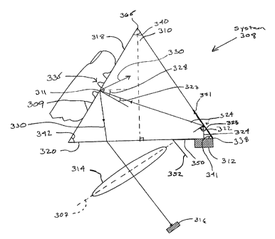
Figures 4 and 5 show a patterned object image acquisition system 308 in
accordance
with the present invention. Acquisition system 308 preferably includes a
triangular prism
310, a light source 312, a lens assembly 314, and an image sensor 316. Prism
310 is a five
faced isosceles triangular prism the length of which extends into the plane of
Figure 4.
Prism 310 includes a rectangular imaging surface 318 against which an object
to be
imaged, such as a fingerprint 335, is placed. Prism 310 also includes a
rectangular viewing
surface 320 through which an image of a fingerprint 335 placed against imaging
surface
318 passes out of prism 310. In the embodiment of Figures 4 and 5, viewing
surface 320
11
CA 02351086 2001-05-11
WO 00/28469 PCT/US99/27051
also serves as a light receiving surface for allowing light to pass into prism
310. A light
scattering surface 322 of prism comprises a third rectangular surface of prism
310. For
reasons detailed below, light scattering surface 322 is preferably a
diffusive.
Light source 312 is preferably an elongated LED array consisting of a single
row of
light emitting diodes (LEDs) extending the length (info the plane of Figure 4)
of prism 310.
If such LEDs are used as light source 312, a diffusive cover can be placed
between the
LEDs and viewing surface 320 to provide more even illumination of imaging
surface 318.
It is also within the ambit of the present invention, however, for light
source 312 to be any
other type of light source to provide incident light into prism 310.
Preferably; light source
312 is placed along an edge 338 of prism 310 which is opposite imaging surface
318.
Lens assembly 314 is for receiving scattered light 330 from fingerprint 335
and
focusing scattered light 330 onto image sensor 3I6. Lens assembly 314 can be a
single
lens or, preferably, can consist of multiple lenses. Most preferably, lens
assembly 314 has
a focal length of approximately 13.48 mm and is located approximately I3.5 mm
from
viewing surface 320. Additionally, as shown in Figure 6B which is a schematic
diagram of
one embodiment of lens assembly 314, lens assembly most preferably consists of
three
lenses 904, 906, and 908 whose respective optical axes are aligned on a common
optical
axis 902. Lens 904 most preferably has a diameter of approximately 17.8 mm,
and both
lenses 906 and 908 most preferably have a diameter of approximately 6 mrn. It
is
considered that any number of lenses be included in lens assembly 3 I4.
Image sensor 316 captures optical light images from lens assembly 314 and
converts
them to electrical signals. Image sensor 316 can be a charge couple device
("CCD") or any
other means of converting a light signal into either an analog or digital
electrical signal.
Preferably, image sensor 316 is a complementary metal oxide semiconductor
device. CCD
and CMS image sensors are well known by those skilled in the art. The
electrical signals
generated by image sensor 316 can be processed using known means and used to
compare
input patterns, such as fingerprints. As noted in the Background section, such
signal
processing means are disclosed, fox example, in U.S. Patent Nos. 4,135,147 and
4,688,995,
which have been incorporated by reference.
12
CA 02351086 2001-05-11
WO 00/28469 PCT/US99127051
To create an optical image of fingerprint 335 on image sensor 316, fingerprint
335 is
placed against imaging surface 318. Incident light 324 from light source 3I2
passes
through viewing surface 320 and into prism 310. Because light source 312 is
located
adjacent to edge 338, incident light 324 strikes scattering surface 322. As
noted above
scattering surface 322 is preferably diffusive. As such, a relatively high
portion of incident
light 334 striking scattering surface 322 is internally scattered in prism
310. This scattered
light then strikes imaging surface 318. Even if light scattering surface 322
is not diffusive,
substantially all of incident light 324 will strike scattering surface 322 at
an angle 323
which is greater than the critical angle for scattering surface 322. Thus,
incident light will
reflect off scattering surface 322 and strike imaging surface 318. To enhance
reflection of
incident light off of scattering surface 322 it is contemplated to place a
mirrored face of a
reflecting surface 381 towards scattering surface 322.
Because incident light 324 has been scattered or directly reflected off of
scattering
surface 322, a relatively large percentage of incident light 324 will strike
imaging surface
318 at an angle 327 less than the critical angle 328 of imaging surface 318.
Accordingly,
incident light 324 which strikes imaging surface 318 at a region thereof where
there is a
fingerprint valley 309 will not undergo total internal reflection and will
substantially pass
through imaging surface 318 such that substantially no light hitting an area
of imaging
surface 318 where there is a fingerprint valley 309 will be directed through
imaging surface
322. However, incident light 324 that strikes a region of imaging surface 318
where there
is a fingerprint ridge 311 touching imaging surface 318 will substantially
scatter, producing
scattered light 330. A portion of scattered light 330 will exit prism 310 via
viewing surface
320. Upon exiting prism 3I0, scattered light 330 will diffract into lens
assembly 314 which
will focus scattered light 330 into image sensor 315.
Because incident light 324 can be scattered by scattering surface 322,
incident light 324
provides relatively uniform illumination over imaging surface 318 which
produces a
relatively uniform image. Such a uniform image is desirable because it is
easier to process
and compare with other stored fingerprint data. To further increase the
uniformity of
illumination over imaging surface 318, the portion of viewing surface 320
facing light
source 312 can be streaked by etching lines 370, shown in Figure 5, in viewing
surface 320.
Lines 370 run the length of prism 310 and parallel to apex 338. Lines 370 act
to diffuse
i3
CA 02351086 2001-05-11
WO 00128469 PCT/US99/2705i
light emitted from light source 312 as is passes through viewing surface 320.
As noted
above, this diffusion enhances the uniformity of illumination over imaging
surface 318.
In addition to the components discussed above, image acquisition system 308
preferably also includes a light blocking shield 350 on a portion of light
receiving surface
adjacent to Light source 312. Preferably, light blocking shield runs the
entire length of
prism 310 (into the plane of Figure 4). Light blocking shield 350 is to reduce
the amount
of stray light from light source 312 which might enter lens assembly 314 and
interfere with
or cloud a fingerprint image. It is also considered that the surface of light
blocking shield
350 facing the interior of prism 310 be mirrored. This mirroring can act to
desirably
increase the intensity of scattered light incident on imaging surface 318. In
addition to, or
instead of, light blocking surface 350, a second light blocking surface 352
can be placed
between light source 312 and lens assembly 314. Light shield 352 preferably
extends from
viewing surface 320 at an angle to block stray light from light source 312
from entering
lens assembly 314.
Because light source 312 is relatively narrow and located adjacent to edge 338
opposite
from imaging surface 318, substantially all incident light 324 reaching
imaging surface 318
is reflected or scattered off of scattering surface 322. That is, almost no
incident light 324
strikes imaging surface 318 directly from light source 312. To further reduce
the likelihood
of incident light 324 directly striking imaging surface 318, light source 312
is preferably
configured not to extend past a line 360, shown in Figure 5, extending the
length of prism
3 I O and defined by the intersection of a plane normal to viewing surface 320
and
intersecting with edge 365, adjacent to imaging surface 318. If light source
312 is kept on
the same side of this line as apex 338, then substantially no incident light
324 emitted
perpendicularly from light source 312 will directly strike imaging surface
318.
By minimizing incident Light 324 from light source 312 that is directly
incident on
imaging surface, there is substantially no total internal reflection of
incident light 324 from
regions of imaging surface 318 where there are fingerprint valleys 309. This
means that
relatively little light from these valley regions passes through viewing
surface 320 and into
lens assembly 314. Rather, substantially all the light passing into lens
assembly 314 from
imaging surface 318 is scattered from fingerprint ridges 31 I on imaging
surface 318. This
14
CA 02351086 2001-05-11
WO 00/28469 PCTIUS99/27051
provides a fingerprint image having relatively high contrast between
fingerprint ridges 311
and valleys 309. Such a high contrast fingerprint image is relatively easy to
process and
compare with other fingerprint images and can, therefore, advantageously
increase
processing accuracy.
Further, use of this scattering technique for image acquisition is achieved
with a
triangular prism, as opposed to a trapezoidal prism as disclosed in Lougheed,
discussed in
the Background section. Because triangular prisms can be more efficient to
manufacture
than trapezoidal prisms, image acquisition system 308 can advantageously be
relatively less
expensive to manufacture.
Moreover, scattered light generally scatters from an object in many
directions, as
opposed to substantially one direction. Thus, scattered light from an object
can be picked
up and focused by a lens over a wide range of distances without any
significant degradation
in quality of the image near the edges of the image. Accordingly, lens
assembly 314 can be
placed relatively close to viewing surface 320 without significant loss of
image quality.
This advantageously allows the image acquisition system 308 to be relatively
compact.
Additionally, the image acquisition system of the current invention can reduce
trapezoidal distortion. As discussed in the Background section, trapezoidal
distortion is
manifested in an image having dimensions distorted from those of the actual
object being
imaged. Trapezoidal distortion is caused by variation in path length of light
from the
apparent image of an object to lens assembly 314 from one part of the imaged
object to
another. As shown in Figure 6A, however, in image acquisition system 308, the
path
length of scattered light 330 from different points on the apparent image 335'
of fingerprint
335 to lens assembly 314 is substantially the same. Specifically, path AA' is
substantially
equal to path BB' and path CC'. Thus, trapezoidal distortion can
advantageously be
reduced. As shown in Figure 6A, substantial equalization of paths AA', BB' and
CC' is
facilitated by tilting lens assembly 314 with respect to viewing surface 320.
However,
unlike image acquisition system 108, shown in Figure 1, such tilting of lens
assembly 3I4
does not reduce the intensity of the image reaching image sensor 316. As noted
in the
background section with respect to image acquisition system 108, tilting lens
assembly 114
causes reflected light 130 to strike the first element of lens assembly 314 at
an angle to
CA 02351086 2001-05-11
WO 00/28469 PCT/US99/27051
normal line thereof. This causes greater reflection of reflected light 130
from the surface of
lens assembly 114, thereby undesirably reducing image intensity at image
sensor 116.
However, as noted above, prism 310 is an isosceles prism and preferably has
base
angles 340 and 34I which measure above 45 degrees. The base angle 340 is the
angle at
edge 365, between imaging surface 318 and scattering surface 322, and base
angle 341 is
the angle at edge 338, which is opposite to imaging surface 318. Further,
prism 310
preferably has an index of refraction not equal to 1. Thus, scattered light
330 which strikes
viewing surface 320 refracts away from the normal to viewing surface 320 as it
exits prism
310. As such, by tilting the lens plane 307 of lens assembly 314, scattered
light 330 strikes
lens assembly 314 at substantially 90 degrees. Thus, there is no loss in image
intensity due
to undue reflection of scattered light at the surface of lens assembly 314,
and trapezoidal
can be reduced without loosing image intensity at image sensor 316.
Preferably, base
angles of prism 310 at edges 365 and 338 preferably measure between 50 and 65
degrees
inclusive and most preferably measure either 62 degrees or 63 degrees. If
prism 310 has
base angles of approximately 62 degrees, the index of refraction of prism 310
is preferably
between 1.71 and 1.72 and most preferably approximately 1.713. If prism 310
has base
angles of approximately 63 degrees, prism 310 preferably has an index of
refraction of
between 1.68 and 1.70, and most preferably approximately 1.6935 or 1.6968.
However, it
is contemplated that prism 310 have any index of refraction higher than 1.
Prism 310 can be made of glass, acrylic or any other transparent material
having an
index of refraction different from 1 (that of air). Prisms having the
preferred index of
refraction and angles are commercially available from Shinkwang Ltd. of Seoul,
Korea and
are fabricated of glass having the designation LaK-7 or LaK-8.
Lens assemblies such as Iens assembly 314 are commercially available from
Seoul
Optical Systems Ltd. of Seoul, Korea and are preferably fabricated from a
glass having the
commercial designation of BK7. If more than one element is used in lens
assembly 314, as
shown in Figure 6A, the individual elements can be aligned and spaced by
placing them in
a frame fabricated by plastic molding or any other fabrication means as is
known in the art.
16
CA 02351086 2001-05-11
WO 00128469 PCT/E1S99/27051
Light source 312 preferably consists of four standaxd LEDs positioned in a
straight
array on a circuit board. Powering of LEDs is well known by those skilled in
the art.
Image sensor 316 is preferably a CMOS type sensor and is commercially
available from
Hyudai Electronics of Seoul, Korea, VLSI Vision, Ltd. of San Jose, California,
or
Omnivision Technologies Inc. of Sunnyvale, California.
To secure the components of image acquisition into the relative positions as
shown in
Figure 4, a frame having holding slots for each component can be plastic
molded or
otherwise fabricated. Light source 312 can be either placed in a holding slot
adjacent to
viewing surface 320 or attached direction to viewing surface 320 using
translucent adhesive
as known in the art.
In the embodiment of the present invention shown in Figures 4-6, light source
312 is
located adjacent to viewing surface 320 which is also the light receiving
surface. However,
it is within the scope of the present invention to move light source 312 to
other surfaces of
the triangular prism. One such embodiment wherein the light source is located
adjacent to
a surface other than the viewing surface, is illustrated in Figure 7. As
shown, a image
acquisition system 408 includes an isosceles triangular prism 410, a sight
source 412, a lens
assembly 414, and a image sensor 416. As with prism 310 of image acquisition
system
308, prism 410 includes an imaging face 418 against which a fingerprint 435 is
placed, and
a viewing surface 420 through which an image of fingerprint 435 is projected
onto lens
assembly 414.
However, as shown, light source 412 is placed adjacent to a light receiving
surface 422,
which is different from viewing surface 420. Light source 412 is a relatively
narrow light
source and can be, for example, a single row of LEDs. Light source 412 is
preferably
placed directly adjacent to edge 448, opposite viewing surface 418 and runs
the length of
prism 418 (into the plane of Figure 7). As with light source 312 of image
acquisition
system 308, preferably, no part of light source 412 crosses a line in light
receiving surface
422 defined by the intersection light receiving surface 422 and a plane which
is normal to
light receiving surface 422 and intersects edge 465 opposite to light
receiving surface 422.
17
CA 02351086 2001-05-11
WO 00/28469 PCT/US9912705i
Incident light 424 from light source 412 passes through light receiving
surface 422 and
strikes viewing surface 420. Because the angle of incidence of a substantial
portion
incident light 424 on viewing surface 420 is greater than the critical angle
for surface 420,
incident light 424 will reflect or scatter off of surface 420 and strike
imaging surface 418.
At this point, the operation of image acquisition system 408 is substantially
the same as that
of image acquisition system 308. Incident light 424 strikes imaging surface at
an angle less
than the critical angle for imaging surface 418 projects an image of
fingerprint 435 through
viewing surface 420 and onto lens assembly 414. Lens assembly 414 then focuses
this
image onto image sensor 416.
As noted, incident light 424 scatters or reflects off of viewing surface 420
before
striking imaging surface 418. This advantageously provides for relatively even
illumination of imaging surface 418. Additionally, substantially all incident
light 424
strikes imaging surface 418 at an angle which is less than the critical angle
of imaging
surface 418. Thus, as discussed above with respect to image acquisition system
308, the
image of fingerprint 435 projected through viewing surface 420 is created by
substantially
all scattered light 430. This advantageously allows lens assembly 414 to be
placed
relatively close to viewing surface 420 without substantial image degradation
and provides
a relatively high contrast image of fingerprint 435.
As with image acquisition system 308, image acquisition system 408 can also
include a
light blocking shield 450 on viewing surface 420 running the length thereof
(into the plane
of Figure 7) and adjacent to apex 438. The surface of light blocking shield
424 facing
viewing surface 420 can be opaque, diffusive or mirrored. Additionally, or
alternatively,
image acquisition system 408 can include a second light blocking shield 452
extending
running the length of viewing surface 420 and extending at an angle therefrom.
Both light
blocking shields 450 and 452 serve to prevent degradation of an image of
fingerprint 435
by diminishing the amount of stray light from light source 412 which might
enter lens
assembly 414.
Further, as with image acquisition system 308, the surface of light receiving
surface
422 in the region where light source 412 faces light receiving surface 422,
can be streaked
with lines running the length of surface 422 and parallel to apex 438. Such
lines serve to
18
CA 02351086 2001-05-11
WO 00/28469 PCT/US99/27051
make incident light 424 more diffuse. As explained above, this provides for
more even
illumination of imaging surface 418.
Moreover, isosceles prism 410 preferably includes base angles 440 and 44I
which are
greater than 45 degrees. More preferably, base angles 440 and 441 are between
50 and 65
degrees, inclusive, and most preferably measure either 62 degrees or 63
degrees. Also;
index of refraction of prism 4I0 is preferably greater than 1.5. As such, when
scattered
light 430 passes through viewing surface 420, scattered light 430 will refract
away from a
line normal to viewing surface 420. Thus, as shown in Figure 7, the lens plane
of lens
I O assembly 414 can be tilted with respect to viewing surface 420 to
advantageously reduce
trapezoidal distortion and scattered light 430 will still enter lens assembly
420 substantially
normal to the lens plane. Thus, as with image acquisition system 308, the
intensity of the
image of fingerprint 435 can remain relatively high.
15 The components of image acquisition system 408, including prism 410, light
source
412, lens assembly 4I4 and image sensor 416, can all be the same components as
those of
image acquisition system 308. Also, image system 408 can be fabricated in
substantially
the same manner as image acquisition system 308. In particular, to secure the
components
of image acquisition into the relative positions as shown in Figure 7, a frame
having
20 holding slots for each component can be plastic molded or otherwise
fabricated. Light
source 412 can be either placed in a holding slot adjacent to light receiving
surface 422 or
attached direction to light receiving surface 422 using translucent adhesive
as known in the
art.
25 It is contemplated that the frame and holding slots discussed above be part
of a standard
computer user input device such as, for example, a keyboard, trackball or
mouse. This is to
allow the optical acquisition system of the present invention to be housed in
such a device.
Figures 19-22 show an embodiment of the present invention wherein an optical
acquisition
system, such as system 308 or 408, is housed in an otherwise conventional
computer
30 mouse.
Figure 19 is a top view of a computer mouse 910 housing an optical acquisition
system,
such as acquisition system 408. Attached to mouse 910 is a parallel port
connector 920 and
19
CA 02351086 2001-05-11
WO 00/28469 PCT/US99/27051
a conventional computer mouse connector 930. It is also considered that mouse
910
include a serial port connector instead of a parallel port connector. As can
be seen in
Figures 20 and 21, which show a perspective view and a side view,
respectively, of mouse
910, imaging surface 418 of prism 410 can be exposed on one edge of mouse 910.
This
allows a user to place a thumb or finger against imaging surface 418 when
using mouse 910
to allow a fingerprint image to be captured by a computer to which mouse 910
is
connected. Figure 22 is a partially cutaway, top view of mouse 910 showing
image
acquisition system 408 housed therein. As shown, image acquisition system 408
is held in
place in mouse 910 by frames 917 retaining prism 410, lens assembly 414, and
image
sensor 416. Additionally, a signal conduit 406, which can be an electrical
wire, runs from
image sensor 416 to detection electronics (not shown).
As noted above, image acquisition system 308 can advantageously be made
relatively
compact. This facilitates placement of image acquisition system 308 in mouse
910. In a
presently preferred embodiment, computer mouse 910 includes both a horizontal
guide 911
and a vertical guide 912 for insuring that a finger whose fingerprint image is
to be taken is
properly aligned in the horizontal and vertical directions, respectively, with
respect to
imaging surface 318. In some embodiments of the computer mouse, use of only
one of the
horizontal and vertical guides may be sufficient for aligning the finger with
the optical
prism. In Figure 21, vertical guide 912 is shown as being near the bottom of
the computer
mouse 910. In an alternative embodiment, vertical guide 912 may be located
near the top
of computer mouse 910 (or, equivalently, imaging surface 418) rather than the
bottom as
shown in Figure 21.
As noted above, mouse 910 is coupled to a parallel connector 920 and a
conventional
computer mouse connector 930. The parallel connector 920 transmits fingerprint
capture
data from the optical structure to a computer to which the pointing device is
coupled. The
conventional mouse port connector transfers power and other signals related to
conventional mouse operation, between the computer mouse 910 and a computer
(not
shown) to which the computer mouse 910 is coupled. The conventional mouse port
connector 930 may be a PS/2 port connector. It is also contemplated that the
mouse port
connector 930 not be used and that only a universal serial bus connector be
used in place of
the parallel connector 920.
CA 02351086 2001-05-11
WO 00/28469 PCT/US99127U51
Although the above description has been made in relation to a computer mouse,
it is to
be noted that the optical structure of the present invention may be used in
conjunction with
numerous other devices. Specifically, the optical structure inay be
incorporated into
telephones, televisions, cars, doors, and other items. The fingerprint image
may be used as
a security access key by the aforementioned items and may be used as a
security access key
or password for accessing a computer system, either upon booting the computer
or when
reentering a computer system from a screen saver.
Another embodiment of the present invention having the light source in yet a
different
location is shown in Figures 8-10. Figure 8 is a side view of an image
acquisition system
508 which, like image acquisitions systems 308 and 408, includes an isosceles
triangular
prism 510, a lens assembly 514, and a image sensor 516. As with prism 310 of
image
acquisition system 308, prism 510 includes an imaging face 518 against which a
fngerprint
535 is placed, and a viewing surface 520 through which an image of fingerprint
535 is
projected onto lens assembly 514. However, as can best be seen in Figures 9
and 10A,
which are, respectively, a perspective view and a front view of prism 510,
image
acquisition system 508 preferably includes at least two separate light sources
512a and
512b each of which are placed over triangular end surfaces 519 and 521 (shown
in Figure
9), respectively, of prism 510. Light sources 512a and 512b are preferably
each an array of
LEDs. However light sources 512a and 5I2b can be any light sources that will
illuminate
the interior of prism 510. It is also contemplated that image acquisition
system 508 include
only one or more than two Light sources.
Operation of light acquisition system 508 is shown in Figure 10A and 10B. As
shown,
incident light 524 emitted from a region of light source 512a near imaging
surface 518 is
incident on imaging surface 518 at an angle greater than the critical angle of
imaging
surface 518. Thus, in regions of imaging surface 518 where there are
fingerprint valleys
509 incident light 524 undergoes total internal reflection and reflected light
530a will strike
triangular surface 521 of prism 510. Reflected light will then either pass
through surface
521, or scatter off of surface 521. On the other hand, incident light 524
which strikes a
fingerprint ridge 511 will primarily undergo scattering, though a relatively
small portion of
such incident light 524 will be absorbed. Scattered light 530b will radiate in
the direction
21
CA 02351086 2001-05-11
WO 00/28469 PCTIUS99/27051
of viewing surface 520 and pass therethrough and into lens assembly 514. As
shown in
Figure 1 OB, which is a partial perspective view of prism 510 and light
sources S 12a and
S 12b, the incident light 524 emitted by light source 512a or S 12b near prism
edge 557
between imaging surface 518 and viewing surface 520 will first be totally
internally
reflected off imaging surface 518. Then, because of the proximity of viewing
surface 520
to imaging surface 518 near edge 557, will totally internally reflect off of
viewing surface
520, and not enter lens assembly S 14. Thus, near edge 557, prism 510 acts as
a light guide
and light which exits viewing surface 520 near edge SS7 is substantially all
scattered light
from imaging surface S 18.
Additionally, referring again to Figure 10A, incident light 524' from a region
of light
source S 12a further away from imaging surface 518 will likely strike imaging
surface 518
at an angle less than the critical angle of imaging surface 518. Accordingly,
incident light
524' will create an image of fingerprint 535 in the same way that incident
light 324 and 424
1 S of image acquisition systems 308 and 408, respectively, does. Incident
light 524' tends to
provide illumination for a region of imaging surface S 18 equidistant between
light source
512a and light source S 12b and incident light S24 tends to provide
illumination for a
regions near the edges of imaging surface 518 which are adjacent to end
triangular surfaces
S 19 and 521. In this way, light sources S 12a and 512b provide relatively
even illumination
over the entirety of imaging surface S 18. Thus, image acquisition system S08
can
advantageously generate a relatively uniform image of fingerprint 535.
As discussed above, image acquisition system generates an image of fingerprint
535
with substantially all scattered light. Thus, as with image acquisition system
308 and 408,
the image produced by image acquisition system 508 is relatively high
contrast.
Additionally, as shown in Figure 1 OA, lens assembly S 14 is preferably wide
enough to
extend from triangular face 519 to triangular face 521. Thus, lens assembly
514 can be
placed relatively close to viewing surface 520. This advantageously allows
acquisition
system S08 to be relatively more compact.
Further, prism 510 has base angles 540 and 541 that preferably measure above
50
degrees and more preferably measure between 50 degrees and 65 degrees and most
preferably measure 62 degrees of 63 degrees. Accordingly, as with image
acquisition
22
CA 02351086 2001-05-11
WO 00/28469 PCT/US99/2?051
systems 308 and 408, scattered light 530a and 530b refracts as it exits
viewing surface 520.
This allows lens assembly to be tilted with respect to viewing surface 520 to
reduce
trapezoidal distortion without substantial loss of image intensity.
Though as shown in Figures 8 through 10, Iight sources 514a and 514b can
essentially
be co-extensive with end triangular surfaces 519 and 521, respectively, it is
also
contemplated that light sources located on end triangular surfaces 519 and 52I
of prism S I O
cover only a portion of each surface 5I9 and 521. For example, as shown in
Figures 1 I and
12, the light sources can be relatively narrow strip light sources. Figures I
1 and 12 show
prism 5I0 with strip light sources 572a and 572b attached to triangular
surfaces 519 and
521, respectively. Strip light sources 572a and 572b run along edges 518a and
518b,
respectively, where end triangular surfaces 519 and 521, respectively, meet
imaging surface
5I8. Light sources 572a and 572b are each preferably a single row of LEDs.
However,
any relatively narrow strip light sources that will illuminate the interior of
prism 5I 0 can be
used.
Light sources 572a and 572b operate in a manner similar to light sources 512a
and
5I2b; respectively, to illuminate imaging surface 518. However, because there
is no
portion of light sources 572a and 572b at a region of end triangular surface
relatively distal
from imaging surface 5I8, illumination by light sources 572a and 572b may not
be as
uniform as with light sources 512a and 512b. However, light sources 572a and
572b
otherwise illuminate imaging surface 518 in substantially the same way as
light sources
512a and 512b, thus, all the additional advantages of image acquisition system
508 are
retained. Further, because light sources 572a and 572b are smaller than light
sources 512a
and 512b, respectively, light sources 572a and 572b can advantageously be
relatively less
costly to manufacture and can consume relatively less power. Image acquisition
system
508 can be fabricated in substantially the same manner and with substantially
the same
components as image acquisition systems 308 and 408.
Another embodiment of the present invention which utilizes, as image
acquisition
apparatus 508 does, totally internally reflected light to generate a scattered
light image of a
fingerprint, is shown in Figures 13 and 14. Figure I3 is a side view of an
image acquisition
apparatus 608 including an isosceles triangular prism 610, a light source 6 i
2, a lens
23
CA 02351086 2001-05-11
WO 00/28469 PCT/US99127051
assembly 614 and an image sensor 616. Like prisms 310, 410 and 510, prism 610
includes
an imaging surface 618 against which a fingerprint 635 is placed, a viewing
surface 620
through which an image of fingerprint 635 is projected, and a light receiving
surface 622
through which the interior of prism 608 is illuminated. Light source 612 is
located adjacent
to light receiving surface 622 and, as shown in Figure I4 which is a
perspective view of
prism 610 including light source 612, can be essentially co-extensive
therewith. Lens
assembly 614 picks up an image of fingerprint 635 and focuses the image onto
image
sensor 616.
In a manner similar to that of image acquisition apparatus 508, incident light
624 from
light source 612 strikes either a region of image surface 618 where there is a
fingerprint
ridge 611 or a fingerprint valley 609. Preferably, apex angle 642 of prism 610
opposite
light receiving surface 622 is small enough such that imaging surface 618 is
close enough
to viewing surface 620 to create a light-guide effect in prism 610. That is,
if imaging
surface S 18 is close enough viewing surface 620, incident light 624 striking
a region of
image surface 618 where there is a fingerprint valley 609 will strike imaging
surface 618 at
an angle greater than the critical angle and undergo total internal
reflection. Totally
internally reflected light 630a will then strike viewing surface 620 and
rather than passing
through viewing surface 620 and into lens assembly 614, will once again
undergo total
internal reflection. This will continue until the totally internally reflected
light 630a is
either entirely attenuated or exits prism 610 through apex 665 opposite to
light receiving
surface 622. However, incident light 624 striking a region of image surface 6I
8 where
there is a fingerprint ridge 611 will primarily scatter off fingerprint ridge
611. A portion of
this scattered light 630b will exit prism 610 through viewing surface 620 and
be picked up
by lens assembly 614 which will focus scattered light 630b onto image sensor
616. Thus,
the image of fingerprint 635 will be relatively bright at fingerprint ridges
611 and relatively
dark at fingerprint valleys 609.
In the manner described above, prism 610 acts essentially as a light guide to
contain
incident light 624 which is not scattered by a fingerprint ridge 611 and
creates an image of
fingerprint 635 using primarily scattered Light. Accordingly, an image
generated by image
acquisition system 608 will have relatively high contrast and can be made
relatively
compact by placing lens assembly 614 relatively close to viewing surface 620.
24
CA 02351086 2001-05-11
WO 00128469 PCTIUS99127051
Moreover, isosceles prism 610 preferably includes base angles 640 and 641
which are
greater than 50 degrees. Also, index of refraction of prism 410 is preferably
greater than 1.
As such, when scattered light 630 passes through viewing surface 620,
scattered light 630
will refract away from a line normal to viewing surface 620. Thus, as shown in
Figure 13,
the lens plane of lens assembly 614 can be tilted with respect to viewing
surface 620 to
advantageously reduce trapezoidal distortion and scattered light 630 can still
enter lens
assembly 620 substantially normal to the lens plane. Thus, as with image
acquisition
system 308, 408 and 508 the intensity of the image of fingerprint 635 can
remain relatively
high.
It is not necessary that an image acquisition system using a light-guide type
refractors
such as pxism 510 or prism 610 be limited to using a triangular prism. Other
light
refractors which act as light guides can also be used in an image acquisition
system. For
example, Figures 15 and 16 shows a side and top view, respectively, of an
image
acquisition system 708 including a circular concave lens 710; light sources
712a, 712b, and
712c; lens assembly 714; and image sensor 716. Concave lens 710 includes a
concave
imaging surface 718, a flat viewing surface 720, and a circular light
receiving surface 722.
Light sources 712a, 7I2b and 712c are preferably equidistantly spaced about
the
circumference of light receiving surface 722. It is also contemplated that
image acquisition
device include only one, two or more than three lights sources.
In a manner similar to prism 610, concave lens 710 acts a light-guide. In
particular
incident light 724 from light sources 712a, 712b, and 7 i 2c strikes imaging
surface 718 at
an angle greater than the critical angle for imaging surface 718. Accordingly,
in regions of
imaging surface 718 where there is a fingerprint valley 709, incident light
724 undergoes
total internal reflection. Reflected light 730 then propagates through concave
lens 710
without passing through viewing surface 722 to enter lens assembly 714. When
incident
light 724 strikes an area of imaging surface 718 where there is a fingerprint
ridge 71 l,
incident light 724 is primarily scattered and some of scattered light 730
passes through
viewing surface 718 and is focused by lens assembly 714 onto image sensor 716.
In this
way, image acquisition system 708 generates an image of fingerprint 735
wherein
fingerprint ridges 711 are relatively bright and fingerprint valleys 709 are
relatively dark.
CA 02351086 2001-05-11
WO 00/28469 PCT/US99/27051
When using an image acquisition surface having a flat imaging surface, a two
dimensional image of a fingerprint could be placed on the imaging surface
rather than an
actual fingerprint. In this way, it could be possible to "trick" the
processing and
comparison apparatus connected to an image acquisition system into registering
a false
match between the two dimensional copy of a fingerprint and a real
fingerprint. However,
imaging surface 718 of lens 710 is concave. Thus, it would advantageously be
more
difficult to place a two-dimensional image of a fingerprint on imaging surface
718 and
thereby "trick" the processing and comparison apparatus connected to image
acquisition
system 708. Additionally, concave imaging surface 718 will more closely match
the
curved contour of a thumb or finger which fingerprint is being imaged. This
means that it
is likely that a higher portion of the surface of a fingerprint will come into
contact with
imaging surface 718, thereby allowing a larger area of a fingerprint to be
imaged. This can
advantageously reduce errors in processing and comparison of fingerprints.
Although the object lens assembly 714 of image acquisition system 708 is
separate
from concave lens 710, it is within the ambit of the present invention for the
first object
lens in lens assembly 714 and concave lens such as lens 710 to be formed as a
single unit.
Such an image acquisition system is shown in Figure 17. Image acquisition
system 808
includes a Lens 810 which has an imaging surface 818 which is concave and a
viewing
surface 822 which is convex. Image acquisition system 808 also includes light
sources
812a, 812b, which are substantially the same as light sources 712a, 712b, and
can include a
third Iight source substantially the same as light source 712c. Image
acquisition system
808 also includes an image sensor 816 and a lens assembly 814 which may or may
not
include an object Lens. It is also contemplated that image acquisition system
808 not
include a lens assembly separate from lens 810. Rather, it is within the scope
of the present
invention to incorporate the lens assembly 814 into lens 810 as a single unit.
Image acquisition system 808 functions in substantially the same manner as
image
acquisition system 708 and, thus, includes all the advantages thereof. It is
also
contemplated that imaging surface 818 of lens 810 be flat rather than concave,
as shown in
Figure 18.
26
CA 02351086 2001-05-11
WO 00/28469 PCT/US99/27051
Many widely different embodiments of the present invention may be constructed
without departing from the spirit and scope of the present invention. It
should be
understood that the present invention is not limited to the specific
embodiments described
in the specification. For example, though the above disclosed embodiments of
the present
invention are described with reference to imaging a fingerprint, any other
type of patterned
object is contemplated to be imaged with the present invention.
27