Note: Descriptions are shown in the official language in which they were submitted.
CA 02355152 2001-06-15
WO 00/36879 PCT/US98/26215
-1-
ELECTROMAGNETIC EXPOSURE CHAMBER
FOR IMPROVED HEATING
FIELD OF THE INVENTION
This invention relates to electromagnetic energy and more particularly to
providing uniform electromagnetic exposure.
BACKGROUND OF THE INVENTION
In recent years, interest in using microwave signals for applications in
many industrial and medical settings has grown dramatically. Some of these
applications include using microwave power for. heat treating various
materials,
polymer and ceramic curing, sintering, plasma processing, and for providing
catalysts in chemical reactions. Also of interest is the use of microwaves for
sterilizing various objects. These applications require electromagnetic
exposure
chambers or enclosures with relatively uniform power distributions. Uniform
power distributions within the chambers help to prevent "hot" or "cold" spots
which may cause unnecessary destruction or waste of sample material. Some of
these applications also require that substances be passed through--rather than
simply placed in--microwave chambers.
The prior art includes various attempts to achieve more uniform exposure
of samples to microwave fields. Commercial microwave ovens utilize "mode
stirrers", which are essentially paddle wheels that help create multiple modes
within a microwave chamber. Many researchers have analyzed the use of
multimode chambers for increasing uniformity of exposure. See Iskander et. al,
FDTD Simulation of Microwave Sintering of Ceramics in Multimode Cavities,
IEEE MICROWAVE THEORY AND TECHNIQUES, Vol. 42, No. 5, May
1994, 793-799. Some have suggested that the limited power uniformity
achievable by mode stirring at a single frequency may be enhanced by using a
CA 02355152 2001-06-15
WO 00/36879 PCT/US98/26215
-2-
band of frequencies. See Lauf et. al, 2 to 18 GHz BroadbandMicrowave Heating
Systems, MICROWAVE JOURNAL, Nov. 1995, 24-34.
Designers have focused on multimode cavities because single mode cavities
are seen as inevitably producing a field with a very limited peak region. See
Lauf
at 24. But multi-mode cavities have yet to produce highly uniform fields
across
an entire cross section of a microwave chamber. Although these cavities result
in
a plurality of field peaks across a chamber, they have many hot and cold
spots.
For every energy peak in such a cavity, there is a corresponding valley.
Attempts
to fill in these valleys with the peaks of waves operating at different
frequencies
creates other problems. The use of large bandwidth swept frequency generators
makes the apparatus expensive and inefficient, since power at some frequencies
will be reflected back to the source.
The possibility of a dielectric slab-loaded structure that elongates the peak
field region in a single mode cavity has been long-but not widely--recognized
See
A.L. Van Koughnett and W. Wyslouzil, A Waveguide TEM Mode Exposure
Chamber, JOURNAL OF MICROWAVE POWER, 7(4) (1972), 383-383.
Koughnett and Wyslouzil disclosed the theoretical existence of a slab-loaded
chamber supporting TEM-mode propagation. However, they did not disclose a
chamber with openings that facilitate the introduction of substances for
exposure
to a relatively uniform electromagnetic field.
A slab loaded structure has been used in a few limited applications as a
microwave applicator. Specifically, a slab loaded guide has been tested for
radiating microwaves into tissue-like samples. See G.P. Rine et. al,
Comparison
of two-dimensional numerical approximation and measurement of SAR in a
muscle equivalent phantom exposed to a 915 MHZ slab-loaded waveguide, INT.
J. HYPERTHERMIA, Vol. 6, No. 1, 1990, 213-225.
Although used in the context of microwave applicators, dielectric slabs
have not been pursued in the context of microwave chambers. In fact, most of
the
CA 02355152 2001-06-15
WO 00/36879 PCT/US98/26215
-3-
prior aft accepts a nonuniform field as a given and attempts to achieve even
heating by other means. For example, a recent sintering patent directed itself
at
wrapping samples in an insulating "susceptor" to uniformly distribute energy
to
samples placed in a nonuniform microwave field. U.S. Patent 5,432,325.
Aside from the problems associated with field uniformity, use of
microwaves in some applications has been limited by concerns over radiation.
Chokes that prevent the escape of electromagnetic energy from the cracks
between
two contacting surfaces are well known in the art. Particularly well known are
chokes designed for microwave oven doors and wave guide couplers. See, e.g.,
U.S. Reissue Patent 32,664 (1988). However, many potential applications
require
a cavity that has access points that are continually open. For these
applications,
substances need to be passed through, rather than placed in, the cavity. The
prior
art has not fully explored the use of choke devices to prevent energy
radiation in
structures that have continually open access points.
In the context of microwave applicators, continually open access points
pose no problem. The goal of such devices is to radiate energy. However, in
the
context of microwave chambers, where the goal is to energize only the space
inside the chamber, continually open access points present potentially harmful
sources of radiation. The problem of radiation through open access points is
magnified as a given and attempts to achieve even heating by other means. For
example, a recent sintering patent directed itself at wrapping samples in an
insulating "susceptor" to uniformly distribute energy to samples placed in a
nonuniform microwave field. U.S. Patent 5,432,325.
Aside from the problems associated with field uniformity, use of
microwaves in some applications has been limited by concerns over radiation.
Chokes that prevent the escape of electromagnetic energy from the cracks
between
two contacting surfaces are well known in the art. Particularly well known are
chokes designed for microwave oven doors and wave guide couplers. See, e.g.,
CA 02355152 2001-06-15
WO 00/36879 PCT/US98/26215
-4-
U.S. Reissue Patent 32,664 (1988). However, many potential applications
require
a cavity that has access points that are continually open. For these
applications,
substances need to be passed through, rather than placed in, the cavity. The
prior
art has not fully explored the use of choke devices to prevent energy
radiation in
structures that have continually open access points.
In the context of microwave applicators, continually open access points
pose no problem. The goal of such devices is to radiate energy. However, in
the
context of microwave chambers, where the goal is to energize only the space
inside the chamber, continually open access points present potentially harmful
sources of radiation. The problem of radiation through open access points is
magnified when the substance being passed through the chamber has any
conductivity. Such conductive substances (e.g., any ionized moisture in paper
that
is passed through a chamber for drying) can, when passed through a microwave
chamber, act as an antenna and carry microwaves outside the cavity.
In many important areas, microwave systems are not in use at all due to
the problems posed by nonuniform fields and the need for continually open
access
points. For example, medical tubing is still sterilized either by chemical
baths or
by electron beam radiation. However, microwave methods have distinct
advantages over electron beam (UV) methods. Microwaves are less likely to
structurally damage the tubing. Also, microwaves can achieve greater depth of
penetration than UV radiation. Therefore, medical tubing is more permeable to
microwaves than to UV radiation. Furthermore, microwaves can kill organisms
and help destroy and remove debris throughout the tubing. UV radiation can
only
kill organisms at or near the tubing's surface but not effectively remove
debris.
Yet microwave structures are not currently employed for pre-use sterilization
of
medical tubing.
CA 02355152 2001-06-15
WO 00/36879 PCT/US98/26215
-5-
SUMMARY OF THE INVENTION
The present invention utilizes dielectric slabs to provide a relatively
uniform
electromagnetic field to a cavity between two or more dielectric slabs. Each
dielectric slab is a thickness equal to or nearly equal to a quarter of a
wavelength
of the electromagnetic field in the dielectric slab.
In a particular embodiment, sample material is introduced into the cavity
between the two dielectric slabs. This sample material may be introduced
through
one or more openings in the dielectric slabs.
In further embodiments, specialized choke flanges prevent the leakage of
energy from this cavity.
In a preferred embodiment, an elliptical conducting surface directs the
electromagnetic field to a focal region between the two dielectric slabs.
Openings
to this focal region allow sample material to be passed through this region of
focused heating.
BRIEF DESCRIPTION OF THE DRAWINGS
The present invention will now be described with reference to the
accompanying drawings in which:
Figure 1 is an electromagnetic exposure chamber in accordance with the
present invention;
Figure 2 is another electromagnetic exposure chamber in accordance with
the present invention;
Figure 3 is another electromagnetic exposure chamber in accordance with
the present invention;
Figure 4 is an illustration of a uniform electromagnetic field in a cross
section of an electromagnetic exposure chamber in accordance with the present
invention;
CA 02355152 2001-06-15
WO 00/36879 PCT/US98/26215
-6-
Figure 5 is an illustration of a relatively uniform electromagnetic field in a
cross section of an electromagnetic exposure chamber in accordance with the
present invention;
Figure 6 is an illustration of another relatively uniform electromagnetic
field in a cross section of an electromagnetic exposure chamber in accordance
with
the present invention;
Figure 7 is an opening in a dielectric slab with a choke flange;
Figure 8 is another opening in a dielectric slab with another choke flange;
Figure 9 illustrates an exemplary embodiment of the present invention that
is particularly useful for sterilizing tubing and other applications.
DETAILED DESCRIPTION OF PREFERRED EMBODIMENTS
Referring now to the drawings, FIG. 1 illustrates an electromagnetic
exposure chamber in accordance with the present invention. The electromagnetic
exposure chamber 10 comprises an exterior surface 11 surrounding dielectric
slabs
12 and 14. Dielectric slabs 12 and 14 may be parallel or not parallel.
The exterior surface 11 and dielectric slabs 12 and 14 form a cavity 16.
The cavity 16 is filled with air or other dielectric material. In a preferred
embodiment, the cavity 16 is filled with Styrofoam to provide stability to the
electromagnetic exposure chamber 10.
The electromagnetic exposure chamber has an opening 17 through which
electromagnetic energy (not shown) is propagated. The opening 17 may be
attached to a traditional waveguide (not shown).
FIG 2. illustrates another electromagnetic exposure chamber in accordance
with the present invention. The electromagnetic exposure chamber 20 comprises
an exterior surface 11 surrounding dielectric slabs 12, 13, 14, and 15.
Dielectric
slabs 12 and 14 may be parallel or may not be parallel. Dielectric slabs 13
and 15
CA 02355152 2001-06-15
WO 00/36879 PCT/US98/26215
-7-
may be parallel or may not be parallel. The dielectric slabs 12, 13, 14, and
15
form cavity 16. The electromagnetic exposure chamber 20 has an opening 17.
FIG 3. illustrates another electromagnetic exposure chamber in accordance
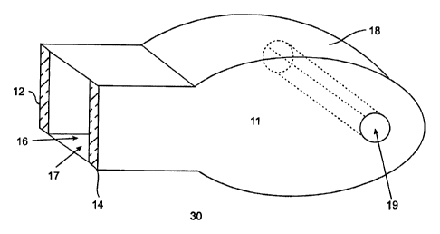
with the present invention. The electromagnetic exposure chamber 30 comprises
an exterior surface 11 and dielectric slabs 12 and 14. The exterior surface 11
has
a continuous, curved side 18 such that the inside surface of said side is an
elliptical surface with a focal region 19. The dielectric slabs 12 and 14 and
exterior surface 11 form a cavity 16. The electromagnetic exposure chamber 30
has an opening 17.
Dielectric slabs 12 and 14 may be formed of titania (Ti02) (Er specified at
96.0 5%). The exterior surface 11 is formed of a conducting material such as
aluminum. It is important that the presence of air gaps be minimized at the
interfaces between exterior surface 11 and dielectric slabs 12 and 14.
FIG. 4 illustrates a uniform electromagnetic field across a dimension of an
electromagnetic exposure chamber in accordance with the present invention. The
magnitude of the electric field 42, 44, and 46 in FIG. 4 is illustrated by
vector
arrows pointing in the vertical direction. The frequency of the
electromagnetic
wave (the operating frequency) can be 915 MHZ, 2.45 GHz, or any other
frequency depending on the desired application.
It is well known in the art that the wavelength X of an electromagnetic
wave at a given frequency depends on the relative dielectric constant E, of
the
material in which the wave exists. This dependence is given by the equation
;L=(3x 10⁸m/s) =(f)(E,)12. Since the E, of the dielectric slabs is greater
than the E,
of the cavity, the wavelength of the electromagnetic field 42 and 44 in the
slab
material 12 and 14 is less than the wavelength of the electromagnetic field 46
in
the material in the cavity 16.
In a preferred embodiment, the electromagnetic exposure chamber is
designed for and operated at the same frequency (i.e., the operating frequency
is
CA 02355152 2001-06-15
WO 00/36879 PCT/US98/26215
-8-
equal to the design frequency). The electromagnetic exposure chamber is
designed such that the thickness t of slabs 12 and 14 are each equal to a 1/4
of the
wavelength of the electromagnetic field 42 and 44 in the slabs 12 and 14. A
1/4
wavelength is the distance between a point in the mode where the magnitude of
the
electric field is equal to zero and the next nearest point in the mode where
the
magnitude of the electric field is at a maximum.
Choosing a slab of thickness slightly greater or slightly less than a 1/4 of a
wavelength does not depart from the spirit of the present invention. As FIG. 5
illustrates, if the thickness t of slab 12 or 14 is slightly greater than 1/4,
the peak
of the electric field occurs within the slab 12 or 14 rather than at the edge
of slab
12 or 14. As FIG. 6 illustrates, if the thickness t of slab 12 or 14 is
slightly less
than X/4, then the peak of the electric field within cavity 16 exceeds the
magnitude of the field at the edge 43 or 45 of the cavity 16, but is still
relatively
uniform across the cavity 16. Both FIG. 5 and FIG. 6 illustrate a relatively
uniform electromagnetic field in a cross section of an electromagnetic
exposure
chamber in accordance with the present invention. Therefore, the phrase "equal
to a 1/4 of a wavelength" is hereinafter intended to mean equal to or about
equal
to a 1/4 of a wavelength.
An advantage of the present invention is that the electric field is at a
maximum at the inside edge 43 or 45 of the dielectric slab 12 or 14 (the
outside
edges of the cavity 16) and is uniform (or nearly uniform) throughout the
cavity
16.
Because the electric field is at a maximum (or near a maximum) at the
outside edges 43 and 45 of the cavity 16, the usable volume of the cavity is
increased. In other words, the peak of the electromagnetic field is wider. In
a
cavity without dielectric slabs 12 and 14, the peak of the electromagnetic
field is
narrow. That is, the magnitude of the electromagnetic field significantly
decreases
at the outside edges 43 and 45 of the cavity 16.
CA 02355152 2001-06-15
WO 00/36879 PCT/US98/26215
-9-
It will be appreciated by those skilled in the art that the electromagnetic
exposure chamber should also be designed and operated such that the
electromagnetic wave is in a singular mode. The best way to ensure that the
electromagnetic wave is in a singular mode is to limit the overall width w.
(Width
w combines the width of the cavity 16 and the thicknesses t of the dielectric
slabs
12 and 14).
If the overall width w is held constant, the width of the cavity 16 (and
hence cavity 16's usable volume) will be maximized by minimizing the width of
the dielectric slabs 12 and 14. It will be appreciated by those skilled in the
art that
a 1/4 of a wavelength at a given frequency is relatively smaller in a material
that
has a relatively large dielectric constant. Therefore, the width of the cavity
16 is
maximized if the relative dielectric constant of the dielectric slabs 12 and
14 is
increased. In sum, if the dielectric constant of the slabs is increased, the
thickness
t of the dielectric slabs 12 and 14 is decreased and the width of the cavity
16 is
increased.
To insure that the electromagnetic wave will operate in a singular mode,
the overall width w should be equal to or less than 2t[1 +(E r1/Er2 - 1)"],
where
Er, is the dielectric constant of the dielectric slabs 12 and 14, Er2 is the
dielectric
constant of the material in the cavity 16, and 2t is the combined thickness of
the
dielectric slabs 12 and 14.
FIG. 5 illustrates a relatively uniform electromagnetic field in a cross
section of an electromagnetic exposure chamber in accordance with the present
invention. As mentioned above, the electromagnetic exposure chamber should be
designed and operated at near the same frequency. If the electromagnetic
exposure chamber is operated at above the design frequency (or if the
dielectric
slabs 12 and 14 are built too thick), the magnitude at the edge 43 or 45 of
the
cavity 16 is no longer at a maximum. The field shown in FIG. 5 occurs if the
electromagnetic exposure chamber is operated at a frequency slightly greater
than
CA 02355152 2001-06-15
WO 00/36879 PCT/US98/26215
-10-
the design frequency. The peak of the electric field occurs within the slab 12
or
14 rather than at the edge 43 or 45 of the slab 12 or 14. The electric field
46 in
the cavity 16 will exhibit a slight downward bow but will still be relatively
uniform across the cavity 16.
FIG. 6 illustrates another relatively uniform electromagnetic field in a
cross section of an electromagnetic exposure chamber in accordance with the
present invention. The field shown in FIG. 6 occurs if the electromagnetic
exposure chamber is operated at a frequency slightly less than the design
frequency (or if the dielectric slabs are built too thin). The peak of the
electric
field 46 within the cavity 16 exceeds the magnitude of the electric field at
the edge
43 or 45 of the cavity 16, but is still relatively uniform across the cavity
16.
If the electromagnetic exposure chamber is operated at well above the
design frequency (or if width w is too wide), the electromagnetic wave will no
longer be in its singular mode. However, if width w is less than 2t[1 + (E
r1/Er2 -
1)"2], the electromagnetic field will still be in its singular mode.
Referring now to FIGS. 7 and 8, for many applications it may be desirable
to introduce substances into the cavity 16 through openings in one or more of
the
dielectric slabs 12 and 14. It may also be desirable to add a choke flange to
such
openings to prevent the escape of electromagnetic energy from the cavity 16.
Creating an open circuit around the outer perimeter of the opening prevents
the
escape of electromagnetic energy.
FIG 7 illustrates a choke flange 71 appropriate for a circular opening 70.
Choke flange 71 may consist of a hollow or dielectrically filled conducting
structure. Choke flange 71 is shorted to the exterior conducting surface 11 at
a
distance d of X/4 from the outer perimeter of the opening 70. X/4 is measured
with reference to the value of E,of the material inside the hollow or
dielectrically
filled choke flange 71. Although ideally the distance d should be equal to
X/4,
CA 02355152 2001-06-15
WO 00/36879 PCT/US98/26215
-11-
choke flange 71 will still operate in accordance with the present invention if
d is
slightly greater or slightly less than X/4.
FIG. 8 illustrates a choke flange 81 adapted to a rectangular opening 80.
The choke flange 81 may consist of a hollow or dielectrically filled structure
that
is either in the shape of a rectangle (not shown), a piecewise simulation of a
rectangle 81 only, or a modified rectangle 81 and 82 with rounded comers 82.
The modified rectangle 81 and 82 with rounded comers 82 can be formed from a
single piece of metal or separate pieces of metal. In the case of separate
pieces of
metal, the separate pieces of metal may have gaps therebetween.
The choke flange 81 is shorted to the exterior conducting surface 11 at a
distance d of X/4 from the outer perimeter of opening 80. V4 is measured with
reference to the value of E, of the material inside the conducting structure
81.
Again, the distance d may be slightly greater or slightly less than X/4.
Losses
from opening 80's corners will typically be negligible. If desired, however,
these
negligible losses may be further eliminated by designing choke flange 81 to
include rounded comers 82 of radius d short circuited at a distance d equal to
or
nearly equal to X/4 from opening 80's comers.
Other shapes for opening/choke flange combinations will depend on the
application. The choice of choke flange shape will depend on the opening shape
which in turn will depend in part on the shape of the substance to be
introduced
into cavity 16.
FIG. 9 illustrates an exemplary embodiment of the present invention that is
particularly useful for sterilizing tubing and other applications. A side 18
of
exterior conducting surface 11 is formed in an elliptical shape. The
elliptical
shape of side 18 reflects the electromagnetic field to a focal region 19. A
circular
opening 70 is at a distal end of the focal region 19. A substance, such as
tubing,
may then be introduced into the focal region 19 of cavity 16 for exposure to a
CA 02355152 2001-06-15
WO 00/36879 PCT/US98/2621 S
-12-
relatively uniform electromagnetic field. The embodiment illustrated in FIG. 9
is
well adapted for sterilizing test tubes, or other elongated objects.
A single mode electromagnetic field may be delivered to the cavity by
means well known in the art. To achieve the full benefits of uniform exposure
in
the preferred embodiment, the field should be polarized so that the electric
field is
oriented perpendicular to the longitudinal axis of the focal region.
In another embodiment, a tapered (i.e. gradually increasing in width)
waveguide (not shown) is used to deliver the electromagnetic wave (not shown)
from a traditional waveguide (not shown) to the opening 17 of the
electromagnetic
exposure chamber. In some embodiments the width of the cavity 16 will exceed
that of the waveguide.
In a further embodiment the dielectric slabs 12 and 14 extend into the
horned waveguide in which case the dielectric slabs 12 and 14 are not
parallel. If
the dielectric slabs 12 and 14 are not parallel, this increases the usable
volume of
the cavity 16 and elongates the focal region 19.
This embodiment and other embodiments are also useful for sintering.
Sintering often requires the heating of substances with relatively high
melting
points. Microwave heating offers the possibility that the heating times
required
for sintering may be significantly reduced. However, a substance to be
sintered
must be heated relatively evenly to permit even densification and to avoid
cracking. For a discussion of temperatures and hold-times associated with the
sintering of selected substances, see the disclosure of U.S. Patent 5,432,325
incorporated herein by reference.
Another specialized application of the present invention relates to exposing
substances to an electromagnetic field for the promotion of thin film
deposition.
For example, rapid thermal processing (RTP) of semiconductor wafers requires
relatively uniform, but rapid, heating. For a discussion of wafer processing,
see
S. Wolf and R.N. Tauber SILICON PROCESSING FOR THE VLSI ERA (1986),
CA 02355152 2001-06-15
WO 00/36879 PCT/US98/26215
-13-
incorporated herein by reference. The present invention enables enhanced field
uniformity for helping to promote more uniform thin-film deposition in the
context
of semiconductor processing and in other thin-film deposition contexts.
Numerous variations or modification of the disclosed invention will be
evident to those skilled in the art. It is intended, therefore, that the
foregoing
description of the invention and the illustrative embodiments be considered in
the
broadest aspects and not in a limited sense.