Note: Descriptions are shown in the official language in which they were submitted.
CA 02355796 2004-05-12
279~57-27
SIGNAL TRANSMITTER HAVING VOLTAGE BOOSTER CIRCUIT AND
METHOD OF OPERATING THE SAME
CROSS REFERENCE TO RELATED APPLICATION
This application is based on Japanese Patent
Application No. 2000-300141 filed on September 29, 2000.
BACKGROUND OF THE INVENTION
The present invention relates to a signal
transmitter, which is suitable for employment, for example,
of keyless entry system for vehicles, and a method of operating
the signal transmitter.
In a keyless entry system installed, for example,
in an automobile, doors of an automobile are usually locked
or unlocked with transmission of data by using radio signals.
Here, the signal transmitter includes a voltage booster circuit
for the stable transmission of radio signal. An output voltage
of a small capacity battery such as a button battery or the
like is boosted up to a predetermined voltage higher than such
an output voltage. Thereby, the data is transmitted using the
radio signal with such a boosted voltage Vb.
However, if the output voltage of the battery is
lowered due to deterioration by aging of the battery, difference
between the output voltage and the predetermined boosted
voltage Vb increases . Thereby, since a large amount of power
of battery is consumed when the output voltage is boosted by
-1-
CA 02355796 2001-08-16
the voltage booster circuit, the output voltage of the battery
which is a power supply voltage of a microcomputer momentarily
becomes lower than the lower limit value of the operation
voltage range of the microcomputer. As a result, it is likely
that the microcomputer can no longer operate normally and
operation life of the signal transmitter may be shortened.
It is therefore proposed to intermittently control
the boosted voltage of the voltage booster circuit at fixed
intervals by a microcomputer. Thus, the voltage booster
circuit provides intermittently periods where the battery
power is not consumed so that the output voltage of battery
does not lower the lower limit value of the operation voltage
range of the microcomputer. The boosted voltage gradually
rises and reduction of the output voltage of the battery is
reduced. However, it is insufficient to only intermittently
control the boosted voltage of the voltage booster circuit at
fixed intervals.
First, the voltage boosting characteristic of the
voltage booster circuit is not uniform because of difference
of specifications and fluctuation in manufacture. Therefore,
the starting time of voltage boosting is different depending
on the voltage booster circuit employed. Moreover, this
starting time of voltage boosting changes depending on
temperature. Therefore, difference arises in the degree of
reduction of the output voltage of the battery during the
voltage boosting operation depending on the voltage booster
circuit employed.
-2-
CA 02355796 2001-08-16
This point will be explained in detail with reference
to Figs . 7A to 7C, which show variation in operation of different
voltage booster circuits. It is assumed in these figures that
a voltage boosting control signal Vbc is outputted to a voltage
booster circuit from a microcomputer in order to instruct the
voltage booster circuit to execute the voltage boosting
operation. This voltage booster circuit boosts a battery
voltage VB by oscillating operation during the period where
the voltage boosting control signal Vbc becomes high level.
During the low level period, this voltage booster circuit does
not oscillate. The voltage boosting control signal Vbc is the
same voltage boosting control signal Vbc in the predetermined
period in such a case that the voltage boosting operation of
the voltage booster circuit is controlled by t:he microcomputer.
Although not illustrated here, the voltage boosting
control s ignal Vbc is a repetitive s ignal of a f fixed interval
and is outputted to the voltage booster circuit from the
microcomputer. That is, the high level period and low level
period of the voltage boosting control signal Vbc are fixed.
Here, Fig. 7A illustrates the change of the
oscillation pulse signal Vosc and the boosted voltage Vb of
the voltage booster circuit and reduction in the output voltage
VB of the battery in such a case that the starting time Ts of
voltage boosting of the voltage booster circuit is equal to
the standard time Tss. Fig. 7B illustrates the change of the
oscillation pulse signal Vosc and the boosted voltage Vb of
the voltage booster circuit and reduction in the output voltage
-3-
CA 02355796 2001-08-16
VB of the battery in such a case that the starting time Tse
of voltage boosting of the voltage booster circuit is shorter
than the standard time Tss. Moreover, Fig. 7C illustrates the
change of the oscillation pulse signal Vosc and the boosted
voltage Vb of the voltage booster circuit and reduction in the
output voltage VB of the battery in such a case that the starting
time Tsd of voltage boosting of the voltage booster circuit
is longer than the standard time Tss.
Here, the starting time Ts of voltage boosting means
the period until the voltage booster circuit starts the
oscillating operation from the input of the voltage boosting
control signal Vbc to the voltage booster circuit.
Under the condition that the voltage boosting
control signal Vbc is in the high level in Figs. 7A to 7C, if
the starting time of voltage boosting of the voltage booster
circuit is equal to the shorter time Tse, the number of
oscillating pulses of the oscillation pulse signal Vosc is
larger than the number of oscillation pulses of the oscillating
pulse signal Vosc in the standard time Tss. Therefore, the
boosting degree of the boosted voltage Vb is larger than the
that of the boosted voltage Vb in the case where the starting
time of voltage boosting is equal to the standard time Tss.
However, the reduction degree ( ~Ve) of the output voltage VB
of the battery is larger than D V of the output voltage VB of
the battery in the case where the starting time of voltage
boosting is equal to the standard time Tss.
In addition, when the starting time of voltage
-4-
CA 02355796 2001-08-16
boosting of the voltage booster circuit is equal to the longer
time Tsd, the number of pulses of the oscillating pulse signal
Vosc is less than the number of oscillating pulses of the
oscillation pulse signal Vosc. Therefore, the boosting degree
of the boosted voltage Vb is smaller than that of the boosted
voltage Vb in the case where the starting time of voltage
boosting is equal to the standard time Tss. However, the
reduction degree ( ~Vd) of the output voltage VB of the battery
is also smaller than that of the output voltage VB of battery
when the starting time of voltage boosting is equal to the
standard time Tss.
Accordingly, the longer the starting time of voltage
boosting is, the smaller the reduction degree of the output
voltage VB of the battery becomes . Thereby, the output voltage
VB of the battery does not readily become lower than the lower
limit value of the operation voltage range of the microcomputer.
On the contrary, a longer time is required until the output
voltage rises up to the predetermined voltage. Meanwhile, the
shorter the starting time of voltage boosting is, the larger
the reduction degree of the output voltage VB of the battery
becomes. Thereby, a longer time is not required until the
voltage rises up to the predetermined value. On the contrary,
the output voltage VB of the battery is readily lowered below
the lower limit value of the operation voltage range of the
microcomputer.
Fig. 6 shows a characteristic curve L identifying
the relationship between the starting time Ts of voltage
-5-
CA 02355796 2001-08-16
boosting and the boosted voltage Vb as the qualitative common
characteristic of the voltage booster circuit. This
characteristics is derived from the relationship between the
starting time Ts of voltage boosting of each voltage booster
circuit and the boosted voltage Vb. The characteristic curve
L indicates that fluctuation exists in the characteristic of
each voltage booster circuit but the starting time Ts of voltage
boosting is rather short and almost does not change in the range
where the boosted voltage Vb is low and the starting time Ts
of voltage boosting rapidly becomes long when the boosted
voltage Vb becomes high. It is thus understood that the
starting time Ts of voltage boosting becomes longer when the
boosted voltage Vb becomes near the predetermined voltage
irrespective of the specification of the voltage booster
circuit.
Therefore, when the high level period of the voltage
boosting control signal Vbc is fixed to the constant value (Tc
in Fig. 6), this high level period of the voltage boosting
control signal Vbc matches with the starting time of voltage
booting. Thus, the boosted voltage Vb saturates (L1 in Fig.
6) and does not rise and thereby the boo sted output of the
voltage booster circuit does not reach the predetermined
boosted voltage Vb. This phenomenon arises at a lower boosted
voltage Vb when the high level period of the voltage boosting
control signal Vbc is shorter.
It is understood from the characteristic La shown
in Fig. 6 that when the high level period of the voltage boosting
-6-
CA 02355796 2001-08-16
control signal Vbc is set longer step by step considering that
the starting time of voltage boosting becomes longer for the
boosted voltage Vb on the characteristic curve L, saturation
of the boosted voltage vb can be prevented. It also becomes
possible to prevent that the output voltage of deteriorated
battery momentarily becomes lower than the lower limit value
of the operation voltage range of the microcomputer.
SUMMARY OF THE INVENTION
It is therefore an object of the present invention
to provide a signal transmitter and a method of operating the
same, which can acquire an adequate voltage required for
controlling a voltage booster circuit irrespective of
difference of specifications of voltage booster circuits as
well as fluctuation and change of the voltage boosting
characteristics, even if an output voltage is lowered due to
deterioration of a small capacity battery.
According to the present invention, a voltage
boosting control signal is generated to have a boosting allowing
period and a boosting inhibiting period following the signal
generation allowing period. An output voltage of a battery is
boosted by a switching operation during the signal generation
allowing period, so that a radio signal may be transmitted with
the boosted voltage. The signal generation allowing period is
increased as time passes to increase the number of the switching
operation in each signal generation allowing period.
_7_
CA 02355796 2005-05-19
27957-27
According to one aspect the invention provides for
a signal transmitter comprising: a battery; a voltage
boosting control signal generating means for sequentially
genex-ating a voltage boosting control signal through
application of an output voltage of the battery as a power
source voltage; voltage boosting means including a switching
mean: for generating a switching signal with a switching
operation through input of the voltage boosting control
signal to conduct a voltage boosting operation to boost the
output voltage of the battery to a predetermined voltage
based on the switching signal; and transmitting means
operated with the boosted voltage for transmitting data,
wherein a period of the voltage boosting control signal has
a signal generation allowing period for allowing generation
of the switching signal and a signal generation inhibiting
period following the signal generation allowing period to
inhibit generation of the switching signal, the signal
generation allowing period being increased as time passes to
increase a number of switching signals generated per
genex-ation allowing period, wherein the switching means
genex-ates the switching signal during the signal generation
allowing period of the voltage boosting control signal for
every generation of the voltage boosting control signal and
stop's generation of the switching signal during the signal
generation inhibiting period, and wherein the voltage
boosting means boosts in steps the output voltage of the
battery to the predetermined voltage for every generation of
the ~>witching signal.
According to another aspect the invention provides
for a signal transmitter comprising: a battery; a voltage
boosting control signal generating means for sequentially
generating voltage boosting control signal pulses through
application of an output voltage of the battery as a power
_g_
CA 02355796 2004-05-12
2757-27
source voltage; a voltage boosting means for executing a
switching operation through input of the voltage boosting
control signal and also executing the voltage boosting
operation to boost the output voltage of the battery up to a
predetermined voltage based on the switching operation; and
transmitting means operated with the boosted voltage for
transmitting data as a radio signal, wherein the voltage
boosting control signal generating means sequentially
generates the voltage boosting control signal in a manner
which increases the number of times of the switching
operation of the voltage boosting means as time passes
thereby to recover a drop of the output voltage of battery
caused by the switching operation.
According to another aspect the invention provides
for a method of operating a signal transmitter having a
battery and a signal transmitter circuit operable with an
output voltage of the battery, the method comprising the
steps of: generating a voltage boosting control signal
having an ON-period and an OFF-period at a first fixed
frequency, the ON-period being increased as time passes;
generating a switching pulse at a second fixed frequency
higher than the first fixed frequency during the ON-period of
the voltage boosting control signal so that the switching
pulse is generated at least once in each ON-period of the
voltage boosting control signal; and boosting the output
voltage of the battery in response to the switching pulse so
that the transmitter circuit is operated with the boosted
output voltage.
BRIEF DESCRIPTION OF THE DRAWINGS
The above and other objects, features and
advantages of the present invention become more apparent from
-8a-
CA 02355796 2004-05-12
27957-27
the following detailed description made with reference to the
accompanying drawings. In the drawings:
Fig. 1 is a block diagram of a signal transmitter
according to a preferred embodiment of the present invention;
Fig. 2 is a flow diagram showing a first part of
operations of a microcomputer used in the embodiment;
Fig. 3 is a flow diagram showing a second part of
operations of the microcomputer;
Fig. 4 is a flow diagram showing a third part of
operations of the embodiment;
Fig. 5 is a signal diagram indicating a voltage
boosting control signal of the microcomputer, an oscillation
pulse signal in a voltage booster circuit, a boosted voltage
and a battery output voltage in the embodiment;
Fig. 6 is a graph indicating the relationship
between a starting time of voltage boosting of a voltage
booster circuit and a boosted voltage in a related art; and
Figs. 7A to 7C are signal diagrams showing voltage
boosting control signal, oscillation pulse signal, boosted
voltage and battery output voltage developed with different
starting times in the related art.
DETAILED DESCRIPTION OF THE PREFERRED EMBODIMENT
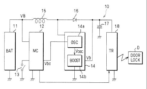
Referring to Fig. 1, a hand-held signal transmitter
-8b-
CA 02355796 2001-08-16
is for a keyless entry system for automobile. This keyless
entry system locks or unlocks the doors of the automobile with
a door-lock device D installed in the automobile using a radio
signal of the signal transmitter 10.
5 The signal transmitter 10 is provided with a battery
(BAT) 11 such as a button-type battery. It may be a small
capacity battery such as a silver battery, a lithium battery
or the like. In this embodiment, a CR2032-type button battery
of nominal voltage VB of 3V and nominal capacity of 220 mAh
10 is used as the battery 11.
The signal transmitter 10 is provided with a
microcomputer (MC) 12. This microcomputer 12 is operated when
a d.c. voltage VB is applied as the power source voltage from
the battery 11. The microcomputer 12 executes, in its
operating condition, a computer program shown in Fig. 2 to Fig.
4 while a start switch 13 is held turned on. During the
execution of the computer program, the processes required for
control of a voltage booster circuit 14 and a transmitter
circuit (TR) 18 are executed. This computer program is stored
in a ROM of the microcomputer 12. The start switch 13 is
composed of a normally-open switch. When this start switch 13
is turned on, the microcomputer 12 is activated.
The voltage booster circuit 14 is provided with an
oscillator circuit ( OSC ) 14a and a voltage booster circuit 14b
as major structural components. The voltage booster circuit
14 allows input of the voltage VB from the battery 11 via a
reactor 15. Upon input of an oscillation control signal
_9_
CA 02355796 2001-08-16
(boosting control signal) Vbc of a first fixed frequency from
the microcomputer 12 , the voltage booster circuit 14 oscillates
and generates an oscillation pulse signal Vosc at every
predetermined period Tl ( Fig . 5 ) . This t:i_me period is so
determined to correspond to a second fixed frequency which is
higher than the first fixed frequency. However, in this
embodiment, the low level period is identica:L to the high level
period in this oscillation pulse signal Vosc. The voltage
booster circuit 14b boosts the voltage VB from the battery 11
via the reactor 15 to a predetermined voltage Vb ( for example,
5V) based on the oscillation output Vosc of the oscillator
circuit 14a.
Here, the voltage booster circuit 14 has the voltage
boosting characteristic which is uniquely determined by the
specifications thereof. This characteristic identifies the
relationship between the starting time Ts of voltage boosting
and the boosted voltage Vb. The oscillator circuit 14a starts
the oscillating operation when the starting time Ts of voltage
boosting has passed after the input of the oscillation control
signal Vbc from the microcomputer 12 (corresponding to the first
falling time of the oscillation pulse signal Vosc). The
reactor 15 operates to control change of the output VB of the
battery 11.
A smoothing capacitor 17 smoothes the boosted
voltage Vb from the voltage booster circuit 14b of the voltage
booster circuit 14 and applies the smoothed voltage to the
transmitter circuit 18. Between thesmoothing capacitorl7 and
-10-
CA 02355796 2001-08-16
reactor 15, a diode 16 is connected. This diode 16 restricts
a reverse flow of current based on the boosted voltage Vb in
the voltage booster circuit 14 to the reactor 15.
The transmitter circuit 18 is provided with a signal
processing circuit and an antenna. This transmitter circuit
18 is rendered operative based on the output voltage from the
smoothing capacitor 17 under the control of the microcomputer
12 . It processes the data ( RF data indicating lock or unlock
of door) from the microcomputer 12 with the signal processing
circuit as the transmitting data and transmits this
transmitting data from the antenna to the door lock device D
using a radio signal. This RF data is a radio frequency data
and the process of the signal process circuit is realized by
generating the transmitting data by modulating the carrier with
the RF data.
The microcomputer 12 executes the program shown in
Figs. 2 to 4.
It repeats determination of NO at step 20 when the
start switch 13 is held turned off. Thereafter, when the start
switch 13 is turned on, the microcomputer 12 determines YES
at step 20 and thereafter starts the voltage boosting control
process routine 30. In this voltage boosting control process
routine 30, the count data N is cleared to 0 (N = 0) at step
31. The pulse signal is outputted at every predetermined
period T1 as the voltage boosting control signal Vbc at step
32.
Here, the voltage boosting control signal Vbc has
-11-
CA 02355796 2001-08-16
the high level pulse width W1 and low level pulse width We as
illustrated in Fig. 5. The pulse width Wl corresponds to a
predetermined time t1, while the pulse width We corresponds
to a predetermined time tc. However, the predetermined time
t1 is set to the value in the range of Ts + 0.5XTo < t1 < Ts
+ To. Here, To is the one cycle period of the oscillation pulse
signal Vosc. Moreover, Ts is the starting time of voltage
boosting of the voltage booster circuit 14. The predetermined
time tc corresponds to the time to recover to the value before
the drop of the voltage VB which is momentarily and repeatedly
lowered due to consumption of power of the battery 11 in each
routine of the subsequent voltage boosting control routines
40 to 120 including the voltage boosting control routine 30.
When the first voltage boosting control signal Vbc
of the period T1 is outputted from the microcomputer 12, the
voltage boosting control signal Vbc is inputted to the
oscillator circuit 14a in the voltage booster circuit 14.
Thereafter the oscillating operation is started after the
starting time Ts of voltage boosting has passed to generate
the oscillation pulse signal Vosc of period To. Here, the
predetermined time t1 corresponding to the pulse width W1 of
the high level of the voltage boosting control signal Vbc is
set to the value in the range of Ts + 0.5XTo < t1 < Ts + To,
only one oscillation pulse signal Vosc is outputted from the
oscillator circuit 14a during the predetermined period t1.
Therefore, in the voltage booster circuit 14, the
voltage booster circuit 14b boosts the voltage VB applied from
-12-
CA 02355796 2001-08-16
the battery 11 via the reactor 15 only as much as the voltage
~Vu (Fig. 5) when the oscillation pulse signal Vosc from the
oscillator circuit 14a rises. Moreover, before this voltage
boosting, the power supplied from the battery 11 via the reactor
15 is consumed in response to the fall of the oscillation pulse
signal Vosc from the oscillator circuit 14a. Therefore, the
voltage VB of battery 11 drops as much as only ~ Va (Fig. 5)
in response to rise of the oscillation pulse signal Vosc from
the oscillator circuit 14a.
The voltage boosting control signal vbc of period
Tl falls with elapse of the predetermined time t1 and maintains
its low level until the predetermined time tc passes. This
predetermined time tc is set to the time which assures recovery
of the voltage VB to the value before drop thereof due to the
power consumption of the battery 11. Therefore, the voltage
VB of the battery 11 is recovered to the value before the drop
thereof from the condition where the voltage VB drops by ~1
Va.
When the process of step 32 is completed, the count
data N is incremented as N - N+1 - 1 at step 33. The
determination at step 34 is NO because N < 1. Thereafter, the
process steps 32 to 34 are repeated until N = 10, that is, until
the boosting control signal Vbc is produced ten times.
Thereby, the voltage boosting by the voltage booster
circuit 14b is repeated in unit of voltage L~Vu until N = 10
based on the voltage VB from the reactor 15 by repeatedly
outputting the voltage boosting control signal Vbc of period
-13-
CA 02355796 2001-08-16
T1. The repetitive rise of the boosted voltage Vb is always
conducted under the recovery condition of the voltage VB of
the battery 11 as explained above. The starting time Ts in the
predetermined time t1 corresponding to each N after N - 2
corresponds to the starting time of voltage boosting of the
voltage booster circuit 14 immediately after N is set.
When the determination at step 34 is YES (N = 10),
the process of the voltage boosting control process routine
40 is started. Thereby, at step 41, the count data N is cleared
to 0 (N = 0) and the pulse signal of the predetermined period
T2 is outputted as the voltage boosting control signal Vbc at
step 42. Here, as illustrated in Fig. 5, the voltage boosting
control signal Vbc of period T2 has the high level pulse width
W2 and low level pulse width We and the pulse width W2
corresponds to a predetermined time t2. However, the
predetermined time t2 is set to the value within the range of
Ts + l.5xTo < t2 < Ts + 2To. Moreover, Ts corresponds to the
starting time of voltage boosting of the voltage booster circuit
14 immediately after the determination at step 34 turns to YES .
when the voltage boosting control signal Vbc of
period T2 is first outputted from the microcomputer 12, the
voltage booster circuit 14 starts the oscillating operation
when the starting time Ts of voltage boosting has passed after
the input of the voltage boosting control signal Vbc from the
oscillator circuit 14a and generates the oscillation pulse
signal Vosc in the period To. Here, the predetermined time t2
corresponding to the high level pulse width W of the voltage
-14-
CA 02355796 2001-08-16
boosting control signal Vbc is set to the value in the range
of Ts + 1.5XTo < t2 < Ts + 2To. Therefore, the number of the
oscillation pulses outputted from the oscillator circuit 14a
during the predetermined time t2 is less than 2 but 1.5 or
larger.
Therefore, in the voltage booster circuit 14, the
voltage booster circuit 14b raises the voltage VB applied from
the battery 11 via the reactor 15 in unit of the voltage c~
Vu for every rise of the oscillation pulse signal Vosc from
the oscillator circuit 14a. Moreover, the power supplied from
the battery 11 via the reactor 15 is consumed, before this
boosting of voltage, for every fall of the oscillation pulse
signal Vosc from the oscillator circuit 14a, the voltage VB
of battery 11 drops twice in unit of the voltage OVa for every
fall of the oscillation pulse signal Vosc from the oscillator
circuit 14a.
The voltage boosting control signal Vbc of period
T2 falls with elapse of the predetermined time t2 and maintains
the low level until the predetermined period tc passes . This
predetermined time tc is set to the time to recover to the value
before the drop of voltage VB even when such voltage VB drops
momentarily with consumption of power of batteryll. Therefore,
the voltage VB of battery 11 is recovered to the value before
the drop of voltage from the condition where the voltage of
2 5 2 O V is lowered .
When the process of step 42 is completed, the count
data N is updated through addition as N = N+1 = 1 at step 43.
-15-
CA 02355796 2001-08-16
At step 44, determination is NO because N < 10. Thereafter,
steps 42 to 44 are repeated until N = 10. Thereby, the boosted
voltage Vb of the voltage booster circuit 14b is boosted
repeatedly in unit of 2~lVu until N = 10 based on the voltage
VB from the reactor 15. The repetitive voltage boosting of the
boosted voltage Vb is always conducted under the condition that
the voltage VB of battery 11 is recovered as explained above.
Ts in the predetermined time t2 corresponding to each N after
N = 2 corresponds to the starting time of voltage boosting of
the voltage booster circuit 14b immediately after the N is set
up.
However, when N = 10 and the determination at step
44 is YES, the process of the next voltage boosting control
routine 50 (Fig. 3) is started. Thereby, the count data N is
cleared (N - 0) at step 51 and the pulse signal of the
predetermined period T3 is outputted at step 52 as the voltage
boosting control signal Vbc. Here, the voltage boosting
control signal Vbc of period T3 has the high level pulse width
W3 and low level pulse width We as illustrated in Fig. 5. The
pulse width W3 corresponds to a predetermined time t3 . However,
the predetermined time t3 is set to the value in the range of
Ts + 2.5xTo < t2 <Ts + 3To.
When the first voltage boosting control signal Vbc
of period T3 is outputted under the control. of microcomputer
12, the oscillator circuit 14a starts the oscillating operation
and generates the oscillation pulse signal Vosc of period To
in the voltage booster circuit 14 when the starting time Ts
-16-
CA 02355796 2001-08-16
of voltage boosting has passed after the voltage boosting
control signal Vbc is inputted to the oscillator circuit 14a.
Here, since the predetermined time t3 corresponding to the high
level pulse width W3 of the voltage boosting control signal
Vbc is set to the value within the range of Ts + 2.5XTo < t3
< Ts + 3To as explained above, the number of oscillation pulse
signals Vosc outputted from the oscillator circuit 14a during
the predetermined t3 is under 3 but is 2.5 or larger.
Accordingly, the voltage booster circuit 14b in the
voltage booster circuit 14 boosts the voltage VB applied from
the battery 11 via the reactor 15 in unit of the voltage ~1
Vu for every rise of the oscillation pulse signal Vosc.
Moreover, since the power supplied from the battery 11 via the
reactor 15 is consumed for every fall of the oscillation pulse
signal Vosc from the oscillator circuit prior to this voltage
boosting, the voltage vB of the battery 11 drops for three times
in unit of the voltage c~Va for every fall of the oscillation
pulse signal Vosc from the oscillator circuit 14a.
The voltage boosting control signal Vbc of period
T3 rises as the predetermined time t3 has passed and remains
at the low level until the predetermined time tc passes . This
predetermined time tc is set, as explained above, to the time
for recovery to the value before drop of the voltage VB even
if such voltage VB is repeatedly lowered momentarily due to
the consumption of the power of battery 11. Therefore, the
voltage VB of battery 11 recovers to the value before the drop
from the value where the voltage 3L~Va is reduced.
-17-
CA 02355796 2001-08-16
When the process of step 52 is completed as explained
above, the count data N is updated through the addition of N
- N+1 at step 53. The determination is NO at step 54 because
N < 10. Thereafter, the steps 52 to 54 are repeated until N
- 10. Thereby, the boosted voltage Vb of the voltage booster
circuit 14b is boosted repeatedly in unit of the voltage
Vu until N = 10 based on the voltage VB from the reactor 15.
The repeated boosting of the voltage is always performed under
the recovery condition of the voltage VB of battery 11 as
explained above. Ts in the predetermined time t3 corresponding
to each N after N = 2 corresponds respectively to the starting
time of voltage boosting of the voltage booster circuit 14
immediately after the setting of N.
The processes of the voltage boosting control
routines 60 to 100 are sequentially conducted. In these
voltage boosting control routines 60 to 100, the processes which
are substantially same as those in the voltage boosting control
routines 30 to 50 are executed except for the following
processes.
That is, in the voltage boosting control routine 60,
a predetermined pulse signal of period T4 is outputted as the
voltage boosting control signal Vbc, while a predetermined
pulse signal of period T5 is outputted as the voltage boosting
control signal Vbc in the routine 70. A predetermined pulse
signal of period T6 is outputted as the voltage boosting control
signal Vbc in the routine 80. A predetermined pulse signal of
period T7 is outputted as the voltage boosting control signal
-18-
CA 02355796 2001-08-16
vbc in the routine 90. A predetermined pulse signal of period
T8 is outputted as the voltage boosting control signal Vbc in
the routine 100.
Here, the voltage boosting control signal vbc of
period T4 has a high level pulse width W4 and low level pulse
width We and the pulse width W4 corresponds to a predetermined
time t4. The predetermined time t4 is set to the value within
the range of Ts + 3.5XTo < t2 < Ts + 4To. The voltage boosting
control signal Vbc of period T5 has a high level pulse width
W5 and low level pulse width We and the pulse width W5
corresponds to a predetermined time t5. However, the
predetermined time t5 is set to the value i_n the range of Ts
+ 4.5xTo < t2 < Ts + 5To.
The voltage boosting control signal vbc of period
T6 has a high level pulse width W6 and low level pulse width
We . The pulse width W6 corresponds to a predetermined time t6 .
However, the predetermined time t6 is set to the value within
the range of Ts + 5.5xTo < t6 < Ts + 6To. The voltage boosting
control signal vbc of period T7 has a high level pulse width
W7 and low level pulse width Wc. The pulse width W7 corresponds
to a predetermined time t7. However, the predetermined time
t7 is set to the value within the range of Ts + 6.5XTo < t6
< Ts + 7To. Moreover, the voltage boosting control signal Vbc
of period T8 has a high level pulse width W8 and low level pulse
width Wc. The pulse width W8 corresponds to a predetermined
time 8. However, the predetermined time t8 is set to the value
within the range of Ts + 7.5XTo < t6 < Ts + 8To.
-19-
CA 02355796 2001-08-16
Therefore, in the voltage boosting processing
routine 60, the output voltage of battery 11 sequentially drops
in unit of the voltage ~lVa for every fall of four times of the
oscillation pulse signal Vosc during the high level of the
voltage boosting controlsignalVbc. Thus, the boosted voltage
Vb is boosted for 10 times in unit of the voltage ~lVu for every
rise of four times of the oscillation pulse signal Vosc. In
the voltage boosting control routines 70 to 100, the number
of times of voltage drops in unit of the voltage c'~V of the output
voltage of battery 11 and the number of times of voltage boosting
in unit of the voltage O Vu of the output voltage of battery
11 increase one by one sequentially. Moreover, such processes
are repeated for 10 times respectively in the voltage boosting
control routines 70 to 100.
When the process of voltage boosting control routine
100 is completed, the processes of the voltage boosting control
routines 110 and 120 (Fig, 4) are sequential:Ly performed. The
processes of the voltage boosting control routines 110 and 120
are substantially similar to above voltage boosting control
routines except for the following processes.
In the voltage boosting control routine 110, the
voltage boosting control s ignal Vbc outputted at step 112 has
a predetermined period T9. This voltage boosting control
signal Vbc has a high level pulse width W9 and low level pulse
width Wc. The pulse width W9 corresponds to a predetermined
time t9. The predetermined time t9 is set to the value within
the range of Ts + 8.5xTo <t6 < Ts + 9To.
-20-
CA 02355796 2001-08-16
Moreover, in the voltage boosting control routine
120, the voltage boosting control signal Vbc outputted at step
122 has a predetermined period T10. This voltage boosting
control signal Vbc has a high level pulse width W10 and low
level pulse width Wc. The pulse width W10 corresponds to a
predetermined time t10. The predetermined time t10 is set to
the value within the range of Ts + 9.5XTo < t6 < Ts + lOTo.
Moreover, in each step 113 , 12 3 in both voltage
boosting control routines 110, 120, N is updated through
addition up to N = 5 . In each step 114 , 124 , the determination
becomes YES when N = 5 . In the voltage boosting control routine
110, number of times of fall of the output voltage of battery
11 in unit of the voltage ~lVa. The number of times of rise
of the output voltage of battery 11 in unit of the voltage O
Vu are larger than that in the voltage boosting control routine
100 by only once. The processes which are larger by only once
are repeated for five times . Moreover, in the voltage boosting
control routine 120, the number of times of fall of output
voltage of battery 11 in unit of the voltage ~lVa. The number
of times of rise of output voltage of battery 11 in unit of
the voltage ~lVu are larger than that in the voltage boosting
control routine 110 by only once. The processes which are
larger by only once are repeated for five times.
When the process of the voltage boosting control
routine 120 is completed, the power source voltage supply
process to the transmitter circuit 18 is executed at step 130.
Therefore, the transmitter circuit 18 is activate to enter the
-21-
CA 02355796 2001-08-16
operating condition based on the smoothing voltage of the
smoothing capacitor 17. At step 140, the output process of RF
data is conducted. Thereby the transmitter circuit 18
processes the output data as the transmitting data with the
signal processing circuit and then transmits this transmitting
data from the antenna using the radio signal as a medium.
Accordingly, the door-lock device D locks and unlocks the doors
of the automobile based on the transmitting data from the
transmitter circuit 18.
As explained above, the high level period of the
voltage boosting control signal Vbc is sequentially set longer
such as the predetermined period t1 to t10 in controlling the
voltage boosting in the voltage boosting control routines 40
to 120 by effectively utilizing the relationship between the
starting time Ts of voltage boosting of the voltage booster
circuit 14 and boosted voltage Vb. Moreover, the low level
period following the high level period is set as the
predetermined period tc. The period from the predetermined
periods t1 to t10 is set so that the number of oscillation pulse
signals Vosc belonging to this period sequentially increases.
The predetermined period tc is set to the period to recover
the voltage drop of battery 11 to the voltage before the voltage
drop. Thereby, even if the output voltage of battery 11 drops
due to deterioration by aging or the like, the output voltage
of battery 11 can be boosted gradually within a short period
of time up to the boosted voltage Vb of the predetermined voltage
by the voltage booster circuit 14 without resulting in that
-22-
CA 02355796 2001-08-16
the output voltage of battery 11 momentarily falls exceeding
the lower limit value {Vth in Fig. 5 ) of the operating voltage
range of the microcomputer 12 during each voltage boosting
operation.
Here, since the number of oscillation pulses Vosc
increases while the predetermined period from t1 to t10 passes,
the number of times of voltage boosting also sequentially
increases. Thereby the voltage boosting may be realized
smoothly within a short period of time.
Moreover, since the high level period of the voltage
boosting control signal Vbc for each input of the voltage
boosting control signal Vbc from the microcomputer 12 to the
voltage booster circuit 14 is longer than the starting time
of voltage boosting when the voltage boosting control signal
Vbc is inputted to the voltage booster circuit 14, the boosted
voltage Vb never saturates.
In addition, since the output voltage of battery 11
is not lowered, even momentarily, than the lower limit value
of the operating voltage range of the microcomputer 12 during
each voltage boosting operation, the microcomputer 12 always
operates normally. As a result, the operation life of the
signal transmitter 10 can be extended intensively.
Moreover, the relationship between thestarting time
Ts of voltage boosting and boosted voltage Vb is effectively
utilized in consideration that the voltage boosting
characteristic of the voltage booster circuit is identified
with the above relationship on the occasion of boosting the
-23-
CA 02355796 2001-08-16
output voltage of battery 11 up to the predetermined voltage
with the voltage booster circuit 14. As a result, even if the
output voltage is lowered due to deterioration of the battery
11, the voltage required for operation of the microcomputer
12 can be assured adequately without fluctuation and change
of voltage boosting characteristic of the voltage booster
circuit 14.
In the embodiment of the present invention, the
oscillator circuit 14a in the voltage booster circuit 14 may
be a switching circuit. It is also possible to realize the
switching operation like the oscillating operation of the
oscillator circuit 14a with such switching circuit.
Moreover, it is possible that a value of N is not
limited to 10 or 5 in each voltage boosting control routine.
The output voltage of battery 11 may be changed within the range
for boosting such output 'voltage to the predetermined voltage
within a short period of time.
Moreover, the low level pulse width of the voltage
boosting control signal Vbc may be widened as much in the voltage
boosting control signal Vbc which is generated later. Moreover,
it is enough when the high level pulse width of the voltage
boosting control signal Vbc is wider as much in the voltage
boosting control routine to be executed later and such pulse
with is never limited to the width explained above.
Moreover, the present invention is not limited to
a the keyless entry system for automobiles, but may be used
as a remote control signal transmitter for air-conditioners,
-24-
CA 02355796 2001-08-16
home electric appliances, building doors and the like.
-25-