Note: Descriptions are shown in the official language in which they were submitted.
CA 02357932 2001-09-27
Attorney Docket No. 53921/177
TITLE: METHOD OF SYNCHRONIZING PARALLEL OPTICAL LINKS
BETWEEN COMMUNICATIONS COMPONENTS
FIELD OF THE INVENTION
The invention relates to a method of synchronizing parallel optical links
between
communications components, such as components of a routing switch platform.
BACKGROUND OF INVENTION
Many switch or router products utilize multiple data interconnection cables or
fiber links
typically called high-speed inter-shelf links (HISLs). Such HISLs may provide
gigabit and
terabit bandwidth capacities between various components within a
communications device. For
example, on a routing switch platform, a HISL may be used to link an interface
card or a line
card circuit to a switch fabric.
In the interest of link throughput, these HISLs may employ parallel optical
interfaces
(PAROLI) and may not use framing overhead. Such framing is generally required
for link
synchronization using conventional methods. Additionally, since PAROLI
interfaces comprise a
plurality of parallel lines, these lines as well as corresponding circuits and
buffers at either end
require proper synchronization with respect to each other.
The link synchronization methods presently available either rely on framing,
or may not
provide satisfactory HISL link alignment of data segments carried on the
PAROLI link. Also,
CA 02357932 2001-09-27
-2-
known prior art solutions do not prevent cells from being sent through the
HISL before it is fully
synchronized, resulting in faulty performance.
Thus, there is a need for a method of synchronizing PAROLI links between
components
of a communications device which is more reliable and robust than methods
available in the
prior art.
SUMMARY OF INVENTION
In an aspect of the invention, there is provided a method of synchronizing
unframed data
flow through parallel optical links between first and second communications
components, each
said first and second communications components including an optical laser for
transmitting
laser signals to the other through said optical links, and each said first and
second
communications components including optical sensors for receiving said
transmitted laser
signals, the method comprising the steps o~
(a) initializing each of said first and second communications components;
(b) enabling said optical lasers and optical sensors and exchanging idle
packets between said
first and second communications components to establish a datapath across said
optical links;
(c) exchanging test data packets across said datapath established in step (b)
to verify
connection of all of said optical links; and
(d) upon verification of connection of said optical links in step (c),
enabling data flow
between said first and second communications components;
whereby, said optical links are synchronized, said datapath is established,
and said test data
transmission is verified before said data flow is allowed between said first
and second
communications components.
20936094.1
CA 02357932 2001-09-27
.r
-3-
In an embodiment, step (a) of the method comprises:
(i) flushing FIFO performed by a device reset and input queues of said first
and second
communications components;
(ii) enable said optical lasers and said optical sensors; and
(iii) latching serial-deserializer circuits operatively connected to said
optical links.
In another embodiment, step (b) of the method comprises:
(iv) enabling said optical laser in said first communications device and
transmitting laser
signals comprising idle packets to said second communications device;
(v) enabling said optical sensor in said first communications device;
(vi) enabling said optical sensor in said second communications device;
(vii) detecting idle packets in said second communications device;
(viii) flushing any queues in said second communications device and detecting
said idle
packets received from said first communications device;
(ix) upon detection of said idle packets from said first communications device
in step (vii),
enabling said optical laser in said second communications device and
transmitting laser signals
comprising return idle packets to said first communications device; and
(x) detecting said return idle packets from said second communications device
using said
optical sensor in said first communications device.
In another embodiment, step (c) of the method comprises:
(xi) generating test data packets in said first communications device and
transmitting said test
data packets across said datapath to said second communications device;
(xii) receiving and enqueuing said test data packets in said second
communications device;
20936094.1
CA 02357932 2001-09-27
-4-
(xiii) testing said dequeued test data packets to verify that they are
properly encoded;
(xiv) upon receiving properly encoded test data packets from said first
communications device
in step (xiii), generating return test data packets and transmitting said
return test data packets
across said datapath to said first communications device; and
(xv) receiving and enqueuing said return test data packets generated in step
(xiii) in said first
communications device;
(xvi) testing said dequeued return test data packets to verify that they are
properly encoded;
and
(xvii) upon receiving properly encoded return test data packets, verifying the
connection of said
optical links.
In a second aspect, the present invention provides a method of resynchronizing
unframed
data flow through parallel optical links between first and second
communications components
upon an occurrence of a communications error therebetween, each said first and
second
communications components including an optical laser for transmitting laser
signals to the other
through said optical links, and each said first and second communications
components including
optical sensors for receiving said transmitted laser signals, the method
comprising the steps o~
(a) detecting a communications error;
(b) upon detection of said communications error in step (a) initializing each
of said first and
second communications components;
(c) enabling said optical lasers and optical sensors and exchanging idle
packets between said
first and second communications components to establish a datapath across said
optical links;
(d) exchanging test data packets across said datapath established in step (c)
to verify
connection of all of said optical links; and
20936094.1
CA 02357932 2001-09-27
-5-
(e) upon verification of connection of said optical links in step (d),
enabling data flow
between said first and second communications components;
whereby, said optical links are synchronized, said datapath is established,
and said test data
transmission is verified before said data flow is allowed between said first
and second
communications components.
In an embodiment, step (b) of the second aspect comprises:
(i) flushing FIFO performed by a device reset and input queues of said first
and second
communications components;
(ii) enabling said optical lasers and said optical sensors; and
(iii) latching serial-deserializer circuits operatively connected to said
optical links.
In another embodiment, step (c) of the second aspect comprises:
(iv) enabling said optical laser in said first communications device and
transmitting laser
signals comprising idle packets to said second communications device;
(v) enabling said optical sensor in said first communications device;
(vi) enabling said optical sensor in said second communications device;
(vii) flushing any queues in said second communications device and detecting
said idle
packets received from said first communications device;
(viii) upon detection of said idle packets from said first communications
device in step (vii),
enabling said optical laser in said second communications device and
transmitting laser signals
comprising return idle packets to said first communications device; and
(ix) detecting said return idle packets from said second communications device
using said
optical sensor in said first communications device.
20936094.1
CA 02357932 2001-09-27
-6-
In another embodiment, step (d) of the second aspect comprises:
(x) generating test data packets in said first communications device and
transmitting said test
data packets across said datapath to said second communications device;
(xi) receiving and enqueuing said test data packets in said second
communications device;
(xii) testing said dequeued test data packets to verify that they are properly
encoded;
(xiii) upon receiving properly encoded test data packets from said first
communications device
in step (xii), generating return test data packets and transmitting said
return test data packets
across said datapath to said first communications device; and
(xiv) receiving and enqueuing said return test data packets generated in step
(xiii) in said first
communications device;
(xv) testing said dequeued return test data packets to verify that they are
properly encoded;
and
(xvi) upon receiving properly encoded return test data packets, verifying the
connection of said
optical links.
In a third aspect, the present invention provides a method of synchronizing
data flow
through parallel optical links between a fabric interface card and a switch
access card, each said
fabric interface card and said switch access card including an optical laser
for transmitting laser
signals to the other through said optical links, and each said fabric
interface card and said switch
access card including optical sensors for receiving said transmitted laser
signals, the method
comprising the steps o~
(a) initializing each of said fabric interface card and said switch access
card;
(b) enabling said optical lasers and optical sensors and exchanging idle
packets between said
fabric interface card and said switch access card to establish a datapath
across said optical links;
20936094.1
CA 02357932 2001-09-27
7
(c) exchanging test data packets across said datapath established in step (b)
to verify
connection of all of said optical links; and
(d) upon verification of connection of said optical links in step (c),
enabling data flow
between said fabric interface card and said switch access card;
whereby, said optical links are synchronized, a datapath is established, and
test data transmission
is verified before data flow is allowed between said fabric interface card and
said switch access
card.
In an embodiment, step (a) of the third aspect comprises:
(i) flushing FIFO performed by a device reset and input queues;
IO (ii) enabling said optical lasers and said optical sensors; and
(iii) latching serial-deserializer circuits operatively connected to said
optical links.
In another embodiment, step (b) of the third aspect comprises:
(iv) enabling said optical laser in said fabric interface card and
transmitting laser signals
comprising idle packets to said switch access card;
(v) enabling said optical sensor in said fabric interface card;
(vi) enabling said optical sensor in said switch access card;
(vii) flushing any queues in said switch access card and detecting said idle
packets received
from said fabric interface card;
(viii) upon detection of said idle packets from said fabric interface card in
step (vii), enabling
20 said optical laser in said switch access card and transmitting laser
signals comprising return idle
packets to said fabric interface card; and
(ix) detecting said return idle packets from said switch access card using
said optical sensor in
said fabric interface card.
20936094.1
CA 02357932 2001-09-27
g
In another embodiment, step (c) of the third aspect comprises:
(x) generating test data packets in said fabric interface card and
transmitting said test data
packets across said datapath to said switch access card;
(xi) receiving and enqueuing said test data packets in said switch access
card;
(xii) testing said dequeued test data packets to verify that they are properly
encoded;
(xiii) upon receiving properly encoded test data packets from said fabric
interface card in step
(xii), generating return test data packets and transmitting said return test
data packets across said
datapath to said fabric interface card; and
(xiv) receiving and enqueuing said return test data packets generated in step
(xiii) in said fabric
interface card;
(xv) testing said dequeued return test data packets to verify that they are
properly encoded;
and
(xvi) upon receiving properly encoded return test data packets, verifying the
connection of said
optical links.
In a fourth aspect, the present invention provides a method of resynchronizing
data flow
through parallel optical links between a fabric interface card and a switch
access card upon an
occurrence of a communications error therebetween, each said fabric interface
card and said
switch access card including an optical laser for transmitting laser signals
to the other through
said optical links, and each said fabric interface card and said switch access
card including
optical sensors for receiving said transmitted laser signals, the method
comprising the steps of:
(a) detecting a communications error;
20936094.1
CA 02357932 2001-09-27
-9-
(b) upon detection of a communications error in step (a) initializing each of
said fabric
interface card and said switch access card;
(c) enabling said optical lasers and optical sensors and exchanging idle
packets between said
fabric interface card and said switch access card to establish a datapath
across said optical links;
(d) exchanging test data packets across said datapath established in step (c)
to verify
connection of all of said optical links; and
(e) upon verification of connection of said optical links in step (d),
enabling data flow
between said fabric interface card and said switch access card;
whereby, said optical links are synchronized, said datapath is established,
and said test data
transmission is verified before said data flow is allowed between said fabric
interface card and
said switch access card.
In a fifth aspect, the present invention provides a method of synchronizing
unframed data
flow through a communications link between first and second communications
components, each
said first and second communications components including a transmitter for
transmitting signals
to the other through said communications link, and each said first and second
communications
includes a receiver for receiving said transmitted signals, the method
comprising the steps of:
(a) initializing each of said first and second communications components;
(b) enabling said transmitters and said receivers and exchanging idle packets
between said
first and second communications components to establish a connection across
said
communications link;
(c) exchanging test data packets across said datapath established in step (b)
to verify
connection of said communications links; and
20936094.1
CA 02357932 2001-09-27
- 1~ -
(d) upon verification of connection of said communications link in step (c),
enabling data
flow between said first and second communications components.
In an embodiment of the fifth aspect, said communications link is a parallel
optical link,
said transmitter is an optical laser, and said receiver is an optical sensor.
In another embodiment of the fifth aspect, the method further comprises the
step of
completing synchronization of said optical links, establishing said datapath,
and verifying said
test data transmission before data flow is allowed between said first and
second communications
components.
In other aspects, the present invention provides various combinations of the
above
aspects.
BRIEF DESCRIPTION OF THE DRAWINGS
The foregoing and other aspects of the invention will become more apparent
from the
following description of specific embodiments thereof and the accompanying
drawings which
illustrate, by way of example only, the principles of the invention. In the
drawings, where like
elements feature like reference numerals (and wherein individual elements bear
unique
alphabetical suffixes):
Fig. 1 is a block diagram of a communications network including a routing
switch platform in which a link synchronization method in accordance
with an embodiment may be used;
Fig. 2 is a block diagram showing high-speed inter-shelf connections between
various communications components within the routing switch platform of
Fig. 1;
20936094.1
CA 02357932 2001-09-27
-11-
Fig. 3A is a block diagram of link synchronization aspects ofthe components of
Fig. 2;
Fig. 3B is a block diagram showing further details of the interface between
the
serial-deserializer of Fig. 3A with other components in the system;
Fig. 4 is a flowchart of steps taken on the fabric interface card of Fig. 3,
in
accordance with an embodiment; and
Fig. 5 is a flowchart of steps taken on a switch access card connected to the
fabric interface card of Fig. 4 by a link, in accordance with an
embodiment.
DETAILED DESCRIPTION OF THE EMBODIMENTS
The description, which follows, and the embodiments described therein, are
provided by
way of illustration of an example, or examples, of particular embodiments of
the principles of the
present invention. These examples are provided for the purposes of
explanation, and not
limitation, of those principles and of the invention. In the description,
which follows, like parts
are marked throughout the specification and the drawings with the same
respective reference
numerals.
The terms as used in this description have the definitions as set out in Table
A, below.
Table A
Term Definition
ASIC Application Specific Integrated Circuit
ATM Asynchronous Transfer Mode
20936094.1
CA 02357932 2001-09-27
-12-
FIC Fabric Interface Card
HISL High Speed Inter Shelf Link
HSC High Speed Shelf Controller
HSPS High Speed Peripheral Shelf
ICON Inter Shelf Connection
IP Internet Protocol
LCS Protocol (PMC The LCS (LineCard to Switch) protocol is
Trademark) a proprietary
communications protocol developed by PMC
Sierra which
runs on an HISL
LPC Line Processing Card
PAROLI Parallel Optical Link/Parallel Optical Interface
PS Peripheral Shelf
Receive
SAC Switch Access Card
SCH Switching Scheduler Card
SS Switching Shelf
SMX Switch Matrix
SSC Switching Shelf Controller
Tx Transmit
Link Is a pair of HISL cabled connections between
a SAC and
FIC. Each cable is a twelve stranded fiber
cable.
Fiber A single strand of twelve that makes up
a HISL cable.
The following is a description of a network associated with a routing switch
platform on
which a method in accordance with an embodiment of the invention may be
practiced.
Referring to Fig. 1, a communication network 100 is shown. Network 100 allows
devices 102A, 102B, and 102C to communicate with devices 104A and 104B through
network
cloud 106. At the edge of network cloud 106, routing switch 108 is the
connection point for
devices 102A, 102B and 102C to network cloud 106. In network cloud 106, a
plurality of
20936094.1
CA 02357932 2001-09-27
-13-
switches 110A, 110B and 1 lOC are connected forming the communications
backbone of network
cloud 106. In turn, connections from network cloud 106 to devices 104A and
104B.
It will be appreciated that terms such as "routing switch", "communication
switch",
"communication device", "switch" and other terms known in the art may be used
to describe
switch 108. Furthermore, while the embodiment is described for switch 108, it
will be
appreciated that the system and method described herein may be adapted to any
switching
system including switches 110A, 1 lOB and 110C.
Switch 108 may be a multi-protocol backbone system which can process, for
example,
both ATM cells and IP traffic through its same switching fabric. Routing
switch 108 may allow
scaling of the switching fabric capacity, for example, from 50 Gbps to 450
Gbps in increments of
14.4 Gbps simply by the insertion of additional shelves into the multi-shelf
switch system. To
enable the exchange of data and status information at such switching fabric
capacities,
corresponding high-speed links are required between various communications
components of
the switch 108.
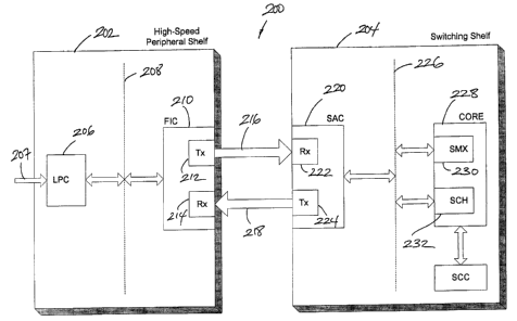
Referring to Fig. 2, the switch 108 may include a switching fabric 200
comprising a
peripheral shelf (PS) 202 and a switching shelf (SS) 204. In operation, the
switching fabric 200
receives data traffic from devices connected to an ingress port of switch 108
(e.g. 112a of Fig. 1),
processes the data traffic through its fabric, then forwards the data traffic
to the correct egress
port of switch 108.
As shown in Fig. 2, each PS 202 may include a line processing card (LPC) 206
which
receives the data traffic from the ingress port 207 of switch 108. The LPC 206
communicates
20936094.1
CA 02357932 2001-09-27
- 14-
via a mid-plane 208 to a fabric interface card (FIC) 210. The FIC 210 includes
a transmit (Tx)
optical device 212 and a receive (Rx) optical device 214, which are connected
to HISL 216 and
HISL 218, respectively. HISLs 216, 218 link the FIC 210 to a switch access
card (SAC) 220 in
SS 204. More specifically, HISL 216 links Tx optical device 212 to a
corresponding Rx optical
device 222 in the SAC 220 which represents the ingress direction of packet
flow into the
switching core. Similarly, HISL 218 links Rx optical device 214 to a
corresponding Tx optical
device 224 in the SAC 220 which represents the egress direction of packet flow
out of the
switching core. The SAC 220 in turn communicates via a mid-plane 226 to a
switching core
228. Within each core 228, there may be up to six switching matrix cards (SMX)
230. Each
SMX card 230 may provide a selectable output stream for data traffic received
through its input
stream. A set of six SMX cards 230 may constitute a non-blocking 32 x 32 HISL
core of the
switching fabric 200. Cell switching both to and from the SAC 220 may be
present and
configured in order to provide an operational switching core 228 for the
switching shelf 204.
Each switching shelf 204 may contain a switching fabric core 228 and up to 32
SACS 220, each
of which may provide, for example, 14.4 Gbps of cell throughput to and from
the core 228.
Still referring to Fig. 2, the HISLs 216, 218 may each provide, for example,
14.4 Gbps
bandwidth. Each HISL 216, 218 may comprise twelve PAROLIs having a capacity of
1.5 Gbps
each. In this case, each HISL 216, 218 would have twelve strands of optical
fiber and the SAC
220 would have twelve dataslices (Fig. 3, below) to handle the queuing of
cells into the
switching core 228. In an embodiment, each cell is segmented amongst the
twelve links. For
example, 6 bytes {48 bits) are transmitted on each fiber for a total of 72
bytes sent in parallel
every 40ns. However, it will be appreciated that the HISL 216, 218 may
comprise other than
twelve PAROLIs and have different throughput capacities or segmentation of
cells.
20936094.1
CA 02357932 2001-09-27
-15-
Now referring to Fig. 3A, a block diagram shows further details of the link
synchronization components in the FIC 210 and SAC 220. Also shown in Fig. 3A
are the
relative points of execution of various steps in a synchronization method for
both the egress and
ingress directions: The FIC process steps are numbered as F0, F1, F2, etc. and
the SAC process
steps are numbered as S0, S1, S2, etc. These steps provide co-ordinated
synchronization of the
HISL. Accordingly, these FIC process steps and SAC process steps may be
independent of each
other and need not know the state of the other end of the HISL 216, 218.
Rather, each process
may rely on sensing the current state of their respective devices and circuits
to determine
whether to move onto the next step. A link synchronization method including
these various FIC
process steps and SAC process steps is described in detail below, with
reference to Fig. 4 and
Fig. 5.
In operation, the FIC 210 may provide encoding/decoding of data, supervise
queue
management of cells to/from the line card/switch fabric, manage backpressure
to/from the line
card, and handle protocol across the HISLs 216, 218 through a specific device.
The data flow from the FIC 210 to the SAC 220 is as follows. In the FIC 210,
the input
data stream from a line processing card 206 is received by an application
specific integrated
circuit (ASIC) 304 which provides encoding/decoding of data, LCS protocol
management, cell
queue management, CRC detection and generation as well as parity checks. For
example, the
ASIC 304 may provide eight bit-to ten-bit (8B/lOB) encoding/decoding. 8B/lOB
encoding will
take an eight-bit cell and map it to a ten-bit cell to disallow continuous
zero or one bit streams.
This is necessary due to the optical devices which require periodic
transitions to properly detect
20936094.1
CA 02357932 2001-09-27
- 16-
ones and zeros. As a non-limiting example, a suitable ASIC is Part No. 34-3626-
00
manufactured by Alcatel Canada Inc.
The ASIC 304 is connected to a plurality of serial-deserializers (Ser/Des)
302a, 302b,
302c which collectively perform a serialization of the data stream arriving as
an input from ASIC
304. The Ser/Des 302a - 302c are connected to a PAROLI Tx optical device 212.
In operation,
the Tx optical device 212 transmits the serialized data stream through the
HISL 216 (comprising
a PAROLI with twelve optical fibers operating at 1.5 Gbps, for example) to Rx
optical device
222 in the SAC 220.
In Fig. 3B, shown is a more detailed view of the interface between the ASIC
304, the
Ser/Des 302a - 302c, the PAROLI Tx 212 and the PAROLI Rx 214 (discussed
below). In an
embodiment, the ASIC 304 is connected to the SerDes 302a - 302c by links
operating at 150
MHz, comprising 12 data slices at 10 bits each. The SerlDes 302a - 302c
perform a 10:1
serialization of the data and have a total of 12 serial links to the PAROLI Tx
212, each running at
1.5 GHz. Similarly, there are a total of 12 serial links from the PAROLI Rx
214 back to the
SerDes 302a - 302c, each link running at 1.5 GHz.
Referring back to Fig. 3A, the serialized data received by Rx optical device
222 is
deserialized by a plurality of Ser/Des 306a - 306c in the SAC 220. The
deserialized data then
feeds into a plurality of dataslices 308 which are used to queue and store
cells processed by the
Ser/Des 306a - 306c. The cells stored in the dataslices 308 may be transferred
to the SMX 230
in the switching core 228 (Fig. 2).
20936094.1
CA 02357932 2001-09-27
- 17-
As a non-limiting example, a suitable dataslice 308 is Part No. PM9313-HC
manufactured by PMC Sierra. This product uses a proprietary LCS (LineCard to
Switch)
protocol. The SAC 220 may further include a port processor 310 that manages
the LCS protocol
across the HISLs 216, 218. While a proprietary protocol has been described by
way of example,
it will be appreciated that other protocols which are capable of operating
across PAROLI links
may be used.
In the return direction from the SAC 220 to the FIC, the data stream from the
SMX 230
in the switching core 228 (Fig. 2) is returned through the dataslices 308 and
into the Ser/Des
306a -306c in the SAC 220. The data stream is serialized in the Ser/Des 306a -
306c and the
serialized data stream is then fed to the Tx optical device 224 for
transmission through HISL 218
back to the FIC 210.
In the FIC 210, Rx optical device 214 receives the data stream from the HISL
218 and
feeds it to the Ser/Des 302a -302c in the FIC 220. The Ser/Des then
deserializes the data stream
and feeds the data stream back to the ASIC 304. The ASIC 304 in turn may pass
the data stream
to an appropriate output port.
Now referring to Fig. 4, shown is a FIC-side process 400 carried out on the
FIC 210 by
the ASIC 304 during HISL 216, 218 synchronization with an SAC 220. The
corresponding
SAC-side process 500 is described further below with reference to Fig. 5.
F0: Initial FIC-side Device and Port State
Step FO shown at block 402 is the initial starting point of process 400. If at
any point in
the method the FIC or port was reset, or if an error was detected during
normal operation, then
20936094.1
CA 02357932 2001-09-27
- 18-
block 402 is the restarting point of process 400, as explained below. From
step F0, process 400
proceeds to step F 1.
F1: Device Initialization and Port Enable
In step F1, shown at block 404, the Tx laser 212 is turned off (otherwise the
SAC 220
may lock into incorrect timing) and all devices in the FIC 210 are reset and
initilized with default
register values. After all devices in the FIC 210 are reset, the HISLs 216,
218 are effectively
shutdown with the Tx laser 212 turned off and the devices disabled. The
initialization in step F 1
removes the devices from reset, initializes encoding/decoding tables, and
enables the ingress and
egress physical layers. Initialization also "latches" the Ser/Des devices 302a
-302c.
Latches are enabled through software writing to the SerDes 302a -302c device
registers
(not shown). When the device latch register is enabled, it locks the SerDes
302a -302c internal
phase lock loop clock to the internal SerDes 302a - 302c transmitter clock.
This starts the Rx
phase lock loop in the SerDes 302a - 302c. Thereafter, the PAROLI Rx 214 is
turned on and the
SerDes 302a -302c will receive incoming idle packets, as described further
below. The idle
packets are detected by the SerDes 302a - 302c in order to properly frame each
incoming packet.
If this latching step is omitted, then the SerDes 302a - 302c will not be
successful in locking onto
incoming packets. SerDes latching is performed in this step F1, and in step S1
described further
below, where Ser/Des 306a - 306c are similarly latched.
Upon execution of step Fl, or in the event of an error or reset instruction
during
execution of step F1, process 400 proceeds to decision block 405. If there is
an error or a reset
instruction, process 400 returns to step FO and the link synchronization
process is restarted.
20936094.1
CA 02357932 2001-09-27
- 19-
Otherwise, process 400 proceeds to step F2. Process 400 is designed to return
to step FO on the
event of an error or reset at any point or step in the process. Therefore
process 400 may be said
to have an automatic restart.
F2: Tx (Transmits Optical Enable
In step F2 shown at block 406, the Tx optical laser 212 is turned on. Once the
Tx optical
laser 212 is on, the FIC 210 begins to transmit idle packets to the SAC 220.
It will be
appreciated that SAC 220 will be undergoing its own link synchronization
process, as described
in detail further below, and must have its Rx optical 222 enabled in order to
receive the idle
packets from the FIC 210. Upon execution of step F2, or in the event of an
error or reset
instruction during execution of step F2, process 400 proceeds to decision
block 407. Block 407
will return process 400 to step FO if there is an error or a reset
instruction. Otherwise, process
400 will proceed to step F3.
F3: Rx Receive) Optical Enable
In step F3, shown at block 408, the FIC 210 enables the Rx optical 214 and
waits to
receive a Tx laser signal from SAC 220. The Rx optical 214 is enabled only
after the Tx laser
signal has been detected. Waiting to enable the Rx optical 214 until this step
helps to prevent
any "dark current" problem which may arise from trying to read a signal that
is not yet being
sent, thus reducing the need for restarting the link synchronization process.
Upon execution of
step F3, or in the event of an error or reset instruction during execution of
step F3, the process
400 proceeds to decision block 409. Block 409 will return the process 400 to
step FO if there is
an error or a reset instruction. Otherwise, the process 400 will proceed to
step F4
20936094.1
CA 02357932 2001-09-27
-20-
F4: Alignment and Idle Packets
In step F4, shown at block 410 when a Rx signal is detected, the FIC 210 ASIC
memory,
tables and test packet detection registers are initialized. Also, the internal
devices of the FIC 210
are placed into operational mode. At this point the devices are waiting for Rx
idle packets from
the SAC 220 on all twelve fiber segments. The ASIC will begin to align itself
to all twelve data
segments while receiving idle packets. More specifically, idle packets do not
necessarily arrive
at precisely the same time on all twelve data segments. The ASIC needs to
ensure the data is
arriving within a certain time period on all twelve segments for it to be
properly aligned. At this
point, assuming that the SAC 220 has progressed to a corresponding step, the
FIC 210 should be
receiving return idle packets from the SAC 220, and be fully aligned to the
data stream coming
from the SAC 220. Upon execution of step F4, or in the event of an error or
reset instruction
during execution of step F4, the process 400 will proceed to decision block
411. Block 411 will
return process 400 to step FO if there is an error or a reset instruction.
Otherwise, process 400
will proceed to step F5.
F5: Test Packet Exchange for HISL Verification
In step F5, shown at block 412, the FIC 210 is now ready to transmit test
packets to the
SAC 220 and to receive return test packets from the SAC 220. Verification
through exchange of
test packets cannot be performed until step FS since a proper datapath is
established only upon
execution of step F4.
In the present embodiment, test packets are cells with a special header that
allows them to
be detected by hardware upon crossing the HISL 216, 218. The test packets may
be written into
20936094.1
CA 02357932 2001-09-27
-21 -
devices in the FIC 210 and SAC 220 and queued for transmission into the data
stream to each
other. Upon arnval, these test packets are dequeued and signal an interrupt to
request service of
the test packet queue. The test packets are then read out of the queues and
analyzed by software
operating on the FIC 210 or on the SAC 220, as the case may be. If the content
in the test packet
is properly encoded, then the HISL 216, 218 is declared to be synchronized.
Otherwise, auto
recovery will engage to try to re-synchronize the link (i.e. the process 400
will return to step FO).
Upon execution of step F5, or in the event of an error or a reset instruction
during
execution of step F5, the process 400 proceeds to decision block 413. Block
413 will return the
process 400 to step FO if there is an error or a reset instruction. Otherwise,
process 400 will
proceed to step F6.
Step F6: HISL is "In Service"
In step F6, shown at block 414, the data flow for the FIC 210 is enabled. Once
the test
packets exchanged in step FS are determined to be valid, the HISLs 216, 218
are put into service
by allowing data flow across. Upon execution of step F6, the FIC-side link
synchronization
process 400 is complete and data can flow between the FIC 210 and the SAC 220.
If an error or
a reset is detected at block 415 during normal operation and transmission of
data flow between
the FIC 210 and the SAC 220, then process 400 will return to step F0. The link
synchronization
process will then restart from block 402, as discussed above.
Now referring to Fig. 5, the SAC 220 executes a corresponding SAC-side link
synchronization process 500. While idle packets and test packets are exchanged
between the
20936094.1
CA 02357932 2001-09-27
-22-
SAC-side process 500 and the FIC-side process 400, the processes are
essentially independent
and may operate by sensing the status of their respective devices.
S0: Initial Device and Port State
Step S0, shown at block 502, is that starting point of the link
synchronization process on
the SAC 220. If the SAC 220 is reset, or if an error is detected during normal
operation, step SO
may also be the restarting point for link synchronization. Upon entering step
S0, the process S00
proceeds to step S 1 to begin the synchronization process.
S 1: Device Initialization and Port Enable
In step S1, shown at block 504, devices in the SAC 220 are reset and
initialized with
default register values. The HISL 216, 218 between the SAC 220 and the FIC 210
is effectively
shutdown as the laser devices in the SAC 220 are turned off and reset. The
initialization in step
S 1 removes the SAC 220 devices from reset, initializes encoding/decoding
tables, enables the
SerDes 306a - 306c, enables the dataslices 308, programs the 8B/lOB tables in
the dataslices
308, puts the port processor into non-operation mode and disables the optical
Tx 224 and optical
Rx 222. However, the optical Rx 222 is able to detect signals in the disabled
mode.
Initialization also "latches" the SerDes 306a -306c, analogously to the SerDes
302a - 302c as
discussed above for step F1.
Upon execution of step S1, or in the event of an error or a reset instruction
during
operation of step Sl, process 500 proceeds to decision block 505. Ifthere are
any errors or reset
instructions, block 505 returns process 500 to step S0. Otherwise, process 500
proceeds to step
S2.
20936094.1
CA 02357932 2001-09-27
- 23 -
S2: Rx (Receive) Optics Enable
In step S2, shown at block 506, the Rx receiver in the SAC 220 is enabled and
the Rx
optical device is tested to determine whether it can detect a laser signal
from the FIC 210. Upon
execution of step S2, or in the event of an error or reset instruction during
execution of step S2,
process 500 proceeds to decision block 507. If there are any errors or reset
instructions, process
500 returns to step S0. Otherwise, process 500 proceeds to step S3.
S3: Alignment and Idle Packets
In step S3, shown at block 508, data-slices 308 (Fig. 4) are checked to
determine if they
can detect the idle packets received from the FIC 210. If the idle packets can
be detected, then
the dataslices 308 are reset to flush any queues that may contain corrupted
cells. Next the
dataslices 308 are checked again to determine if they can detect idle packets.
This is necessary
when the dataslices 308 (e.g. PMC Sierra Part No. PM9313-HC) do not support a
queue flush
function. The only way to flush the queues on the dataslices 308 is to power
them off and back
on again (i.e. a device reset). The first dataslice test is to ensure that the
dataslices 308 can see
any idle packets at all. Then the dataslices 308 are reset to attempt to align
all twelve dataslices
308 to flush the queues of any corrupted cells received beforehand. After a
reset is completed, it
is necessary to retest the queues to ensure that the incoming idle packets are
properly aligned and
not skewed across all twelve slices 308.
To prevent cells from being sent through the HISL 216, 218 before it is
synchronized,
internal switch core links and the port processor 310 are enabled only after
link alignment.
During HISL 216, 218 synchronization, it is undesirable to allow cells to flow
into the switching
20936094.1
CA 02357932 2001-09-27
-24-
core 228. Likewise, the port processor 310 on the SAC 220 can only be enabled
when both
HISL ports 216, 218 that are being synchronized are sending idle packets in
both directions.
This prevents the port processor 310 from communicating with the switch core
scheduler 232
during HISL 216, 218 initialization.
Upon execution of step S3, or in the event of an error or reset instruction
during
execution of step S3, process 500 proceeds to decision block 509. At block
509, if there are any
errors or reset instructions, the process 500 returns to step S0. Otherwise,
the method proceeds
to step S4.
S4: Tx Optical Enable
In step S4, shown at block S 10, the Tx optical device in the SAC 220 is
activated, and in
response to detection of idle packets from the FIC 210 in step S3, return idle
packets are sent to
the FIC 210. Upon execution of step S4, or in the event of an error or reset
instruction during
execution of step S4, process 500 proceeds to decision block 511. At block
511, if there are any
errors or reset instructions, process 500 will return to step S0. Otherwise,
the method will
proceed to step S5.
SS: Enable Switch Core Links and Port Processor
In step S5, shown at block 512, return idle packets are sent to the FIC 210
once the FIC 210 is
properly "aligned" to the SAC 220 idle packets. (Alignment is achieved, for
example, when
twelve independent streams of bits find the start of a six byte sequence (idle
packet) within the
same clock cycle. If any one of the twelve streams fails to find idle packets
or fails to achieve it
in the same clock cycle, then the dataslices 308 are said to be skewed. This
would require a
20936094.1
CA 02357932 2001-09-27
-25-
restart at step S0.) The SAC 220 is adapted to detect this alignment and, upon
its occurrence, the
SAC 220 will enable the switching core links for data flow. The SAC 220 is
also able to detect a
change in idle packets coming from the FIC 210. There are two kinds of idle
packets: The FIC
210 will initially send a first kind of idle packet that indicates that it is
not receiving idle packets
on its Rx device 214. And second kind of idle packet indicates that the FIC
210 is properly
receiving idle packets on its Rx device 214. In this way the SAC 220 can
determine if the FIC
210 is receiving idle packets that are transmitted from the SAC 220.
Thereafter, the idle packet counter is programmed to a lower insertion rate
and an SAC
port processor is enabled to allow the data flow. The port processor then will
be able to
communicate with a scheduler to allow cells queued in the dataslices 308 to
enter the switching
core. Upon completion of step S5, or in the event of an error or reset
instruction during
execution of step S5, process 500 proceeds to decision block 513. If there are
any errors or reset
instructions, process 500 will return to step S0. Otherwise, the method will
proceed to step S6.
S6: Test Packet Exchange for HISL Verification
At step S6, shown at block 514, the SAC 218 is ready to receive and transmit
test
packets. These packets are written into the Port Processor 310 by software and
queued into the
data stream. The port processor 310 will indicate that it received a test
packet which is read out
of its queue and analyzed by software to ensure the packet is valid. Upon
execution of step S6, or
in the event of an error or reset instruction during execution of step S6,
process 500 proceeds to
decision block 515. If there are any errors or reset instructions, process 500
will return to step
S0. Otherwise, the method will proceed to step S7.
20936094.1
CA 02357932 2001-09-27
-26-
S7: HISL is "In Service"
At step S7, shown at block 516, the HISL 216, 218 is put into service by
allowing data
flow across the HISL link. Upon execution of step S7, the link synchronization
process is
complete. During normal operation, if there are any errors or reset
instructions, the process 500
will return to step S0. Upon such an occurrence, the FIC 210 and SAC 220 will
begin to put all
devices into reset and restart the link synchronization process at step S0, as
explained above.
It is noted that those skilled in the art will appreciate that various
modifications of detail
may be made to the present embodiment, all of which would come within the
scope of the
invention. Specifically, any modification of the order of steps taken in
process 400 or in process
S00 which does not substantially affect the link synchronization process is
contemplated to be
within the scope of the present invention. For example, step F3 (Rx Optical
Enable) may be
executed concurrently with step F2 rather than consecutively. Similarly, the
number of steps in
each of process 400 and process 500 is not necessarily limiting, as one or
more steps may be
combined and viewed to be in the same step, or one of the steps described
above may be parsed
into a plurality of steps.
20936094.1