Language selection

Search

Patent 2368386 Summary

Third-party information liability

Some of the information on this Web page has been provided by external sources. The Government of Canada is not responsible for the accuracy, reliability or currency of the information supplied by external sources. Users wishing to rely upon this information should consult directly with the source of the information. Content provided by external sources is not subject to official languages, privacy and accessibility requirements.

Claims and Abstract availability

Any discrepancies in the text and image of the Claims and Abstract are due to differing posting times. Text of the Claims and Abstract are posted:

  • At the time the application is open to public inspection;
  • At the time of issue of the patent (grant).
(12) Patent: (11) CA 2368386
(54) English Title: ANALOG DRIVER FOR LED OR SIMILAR DISPLAY ELEMENT
(54) French Title: CIRCUIT D'ATTAQUE ANALOGIQUE DESTINE A UNE DIODE LUMINEUSE OU A UN ELEMENT D'AFFICHEUR SIMILAIRE
Status: Deemed expired
Bibliographic Data
(51) International Patent Classification (IPC):
  • G09G 3/32 (2016.01)
(72) Inventors :
  • HOLLOMAN, CHARLES J. (United States of America)
(73) Owners :
  • HOLLOMAN, CHARLES J. (United States of America)
(71) Applicants :
  • HOLLOMAN, CHARLES J. (United States of America)
(74) Agent: RIDOUT & MAYBEE LLP
(74) Associate agent:
(45) Issued: 2004-08-17
(86) PCT Filing Date: 1999-03-16
(87) Open to Public Inspection: 1999-09-23
Examination requested: 2001-09-18
Availability of licence: N/A
(25) Language of filing: English

Patent Cooperation Treaty (PCT): Yes
(86) PCT Filing Number: PCT/US1999/005569
(87) International Publication Number: WO1999/048079
(85) National Entry: 2001-09-18

(30) Application Priority Data:
Application No. Country/Territory Date
09/044,581 United States of America 1998-03-19

Abstracts

English Abstract


The analog driver (10) for a display device which is controlled by current,
such as an LED, includes a strobed analog input which
charges a storage capacitor (18). The voltage across the storage capacitor
(18) is fed to the positive input of a comparator (22). The negative
input of the comparator (22) receives the voltage from a feedback resistor
(30) which is in series with the drive voltage, the drive FET (28)
(with a gate connected to the output of the comparator (22)) and the light
emitting device. Additionally, a reset FET (32) is provided in
parallel with the storage capacitor (18). Displays can be manufactured by a
series of panels, each of the panels including an array of these
drivers and light emitting devices, along with appropriate control circuitry.


French Abstract

L'invention concerne un circuit d'attaque analogique (10) destiné à un dispositif d'affichage commandé par le courant, par exemple, à une diode lumineuse LED. Le circuit comprend une entrée analogique à effet stroboscopique qui charge un condensateur de stockage (18). La tension dans le condensateur de stockage (18) alimente l'entrée positive d'un comparateur (22). L'entrée négative du comparateur (22) reçoit la tension provenant d'une résistance à rétroaction (30) qui est couplée en série à la tension d'alimentation, au transistor à effet de champ FET (28) d'alimentation (dont une grille est connectée à la sortie du comparateur (22)) et au dispositif lumineux. En outre, un transistor à effet de champ FET de mise à zéro (32) est connecté en parallèle avec un condensateur de stockage (18). Cette invention permet de fabriquer des afficheurs à partir de plusieurs séries de panneaux, chaque panneau comprenant un réseau de dispositifs lumineux et de circuits d'attaque faisant l'objet de l'invention et possédant des circuits de commande appropriés.

Claims

Note: Claims are shown in the official language in which they were submitted.


CLAIMS

1. A device for controlling current through a light emitting device in
accordance
with an analog informational signal, comprising:
means for receiving the analog informational signal,
means for charging a capacitor in accordance with the analog informational
signal, and
feedback means for controlling current through the light emitting device
through a substantially continuous range thereby varying a brightness of the
light
emitting device through a substantially continuous range in response to
changes in
a voltage across said capacitor responsive to said analog informational
signal.

2. The device of claim 1 further including a first field effect transistor and
a
feedback resistor in series with said light emitting device and wherein said
means
for controlling current includes an operational amplifier with a positive
input, a
negative input and an output; wherein said positive input receives a voltage
substantially equal to the voltage across said capacitor, said negative input
receives
a voltage substantially equal to the voltage across the feedback resistor and
a gate
of said first field effect transistor receives a voltage substantially equal
to the voltage
of said output of said operational amplifier.

3. The device of claim 2 further including a second field effect transistor
for
strobing said analog signal.

4. The device of claim 3 further including a third field effect transistor for
discharging said capacitor.

5. The device of claim 4 further including a resistor to increase a leakage
resistance of said operational amplifier, thereby adjusting an RC time
constant and
modifying a persistence of the device.


6. A device for controlling current through a three color light emitting
device in
accordance with three respective analog informational signals, wherein said
three
color light emitting device includes three respective color circuits, the
device
comprising for each respective analog informational signal:
means for receiving the respective analog informational signal,
means for charging a capacitor in accordance with the respective analog
informational signal, and
feedback means for controlling current through the respective color circuit of
light emitting device through a substantially continuous range thereby varying
a
brightness of the light emitting device through a substantially continuous
range in
response to changes in a voltage across said capacitor responsive to said
respective analog informational signal.

7. The device of claim 6 wherein the device for each respective analog signal
further includes a first field effect transistor and a feedback resistor in
series with
said light emitting device and wherein said means for controlling current
includes an
operational amplifier with a positive input, a negative input and an output;
wherein
said positive input receives a voltage substantially equal to the voltage
across said
capacitor, said negative input receives a voltage substantially equal to the
voltage
across the feedback resistor and a gate of said first field effect transistor
receives a
voltage substantially equal to the voltage of said output of said operational
amplifier.

8. The device of claim 7 wherein the device for each respective analog signal
further includes a second field effect transistor for strobing said respective
analog
signal.

9. The device of claim 8 wherein the device for each respective analog signal
further includes a third field effect transistor for discharging said
capacitor.

11


10. The device of claim 9 wherein the device for each respective analog signal
further includes a resistor to increase a leakage resistance of said
operational
amplifier, thereby adjusting an RC time constant and modifying a persistence
of the
device.

11. A panel including rows and columns of three color light emitting devices,
each
of said three color light emitting device responding in accordance with three
respective analog informational signals, wherein each said three color light
emitting
device includes three respective color circuits, and comprising for each
respective
analog informational signal:
means for receiving the respective analog informational signal,
means for charging a capacitor in accordance with the respective analog
informational signal, and
feedback means for controlling current through the respective color circuit of
light emitting device through a substantially continuous range thereby varying
a
brightness of the light emitting device through a substantially continuous
range in
response to changes in a voltage across said capacitor responsive to said
respective analog informational signal.

12. The panel of claim 11 wherein each light emitting device, further
includes, for
each respective analog signal, a first field effect transistor and a feedback
resistor in
series with said light emitting device and wherein said means for controlling
current
includes an operational amplifier with a positive input, a negative input and
an
output; wherein said positive input receives a voltage substantially equal to
the
voltage across said capacitor, said negative input receives a voltage
substantially
equal to the voltage across the feedback resistor and a gate of said first
field effect
transistor receives a voltage substantially equal to the voltage of said
output of said
operational amplifier.

12


13. The panel of claim 12 wherein each light emitting device, further
includes, for
each respective analog signal, a second field effect transistor for strobing
said
respective analog signal.

14. The panel of claim 13 wherein each light emitting device further includes,
for
each respective analog signal, a third field effect transistor for discharging
said
capacitor.

15. The panel of claim 14 wherein said rows are sequentially provided with
input
data.

16. The panel of claim 15 wherein each light emitting device further includes,
for
each respective analog signal, a resistor to increase a leakage resistance of
each
said respective operational amplifier, thereby adjusting an RC time constant
and
modifying a persistence of the respective device.

17. A display comprised of a plurality of the panels of claim 11.

18. A display comprised of a plurality of the panels of claim 12.

19. A display comprised of a plurality of the panels of claim 13.

20. A display comprised of a plurality of the panels of claim 14.

21. A display comprised of a plurality of the panels of claim 15.

22. A display comprised of a plurality of the panels of claim 16.

23. A device for controlling current through a light emitting device in
accordance
with an analog signal, comprising:
means for receiving the analog signal,

13


means for charging a capacitor in accordance with the analog signal, and
means for controlling current through the light emitting device in accordance
with a voltage across said capacitor;
further including a first field effect transistor and a feedback resistor in
series
with said light emitting device and wherein said means for controlling current
includes an operational amplifier with a positive input, a negative input and
an
output; wherein said positive input receives a voltage substantially equal to
the
voltage across said capacitor, said negative input receives a voltage
substantially
equal to the voltage across the feedback resistor and a gate of said first
field effect
transistor receives a voltage substantially equal to the voltage of said
output of said
operational amplifier.

24. The device of claim 23 further including a second field effect transistor
for
strobing said analog signal.

25. The device of claim 24 further including a third field effect transistor
for
discharging said capacitor.

26. The device of claim 25 further including a resistor to increase a leakage
resistance of said operational amplifier, thereby adjusting an RC time
constant and
modifying a persistence of the device.

27. A device for controlling current through a three color light emitting
device in
accordance with three respective analog signals, wherein said three color
light
emitting device includes three respective color circuits, the device
comprising for
each respective analog signal:
means for receiving the respective analog signal,
means for charging a capacitor in accordance with the respective analog
signal, and

14


means for controlling current through the respective color circuit of light
emitting device in accordance with a voltage across said capacitor;
wherein the device for each respective analog signal further includes a first
field effect transistor and a feedback resistor in series with said light
emitting device
and wherein said means for controlling current includes an operational
amplifier with
a positive input, a negative input and an output; wherein said positive input
receives
a voltage substantially equal to the voltage across said capacitor, said
negative
input receives a voltage substantially equal to the voltage across the
feedback
resistor and a gate of said first field effect transistor receives a voltage
substantially
equal to the voltage of said output of said operational amplifier.

28. The device of claim 27 wherein the device for each respective analog
signal
further includes a second field effect transistor for strobing said respective
analog
signal.

29. The device of claim 28 wherein the device for each respective analog
signal
further includes a third field effect transistor for discharging said
capacitor.

30. The device of claim 29 wherein the device for each respective analog
signal
further includes a resistor to increase a leakage resistance of said
operational
amplifier, thereby adjusting an RC time constant and modifying a persistence
of the
device.

31. A panel including rows and columns of three color light emitting devices,
each
of said three color fight emitting device responding in accordance with three
respective analog signals, wherein each said three color light emitting device
includes three respective color circuits, and comprising for each respective
analog
signal:
means for receiving the respective analog signal,


means for charging a capacitor in accordance with the respective analog
signal, and
means for controlling current through the respective color circuit of light
emitting device in accordance with a voltage across said capacitor;
wherein each light emitting device, further includes, for each respective
analog signal, a first field effect transistor and a feedback resistor in
series with said
light emitting device and wherein said means for controlling current includes
an
operational amplifier with a positive input, a negative input and an output;
wherein
said positive input receives a voltage substantially equal to the voltage
across said
capacitor, said negative input receives a voltage substantially equal to the
voltage
across the feedback resistor and a gate of said first field effect transistor
receives a
voltage substantially equal to the voltage of said output of said operational
amplifier.

32. The panel of claim 31 wherein each light emitting device, further
includes, for
each respective analog signal, a second field effect transistor for strobing
said
respective analog signal.

33. The panel of claim 32 wherein each light emitting device further includes,
for
each respective analog signal, a third field effect transistor for discharging
said
capacitor.

34. The panel of claim 33 wherein said rows are sequentially provided with
input
data.

35. The panel of claim 34 wherein each light emitting device further includes,
for
each respective analog signal, a resistor to increase a leakage resistance of
each
said respective operational amplifier, thereby adjusting an RC time constant
and
modifying a persistence of the respective device.

36. A display comprised of a plurality of the panels of claim 31.

16


37. A display comprised of a plurality of the panels of claim 32.

38. A display comprised of a plurality of the panels of claim 33.

39. A display comprised of a plurality of the panels of claim 34.

40. A display comprised of a plurality of the panels of claim 35.

17

Description

Note: Descriptions are shown in the official language in which they were submitted.


CA 02368386 2004-O1-26
ANALOG DRIVER FOR LED OR~MI l,IISPLA'Y ELEMENT
BA~~ROUND QF THE ~,NVENTION
Field ~f. the Invention '
This invention pertains to an analog memory
driver for all classes of light emitting devices
where the light output is a function of current. The
analog memory driver is a memory unit and driver
Where the current through the display device is
controlled by an analog voltage which is set from an.
analog drive line using a sample and hold circuit.
Description of the Pr,~or Art
Welh-designed current LED drivers currently use
a constant current-drive to compensate for variations
in the forward voltage drop of various LEDs, and
where the current is set by operating voltages or
with current regulators, and the intensity of the LED
is controlled by pulse width modulation. The overall
intensity of the display may be varied by either
selecting alternate pulse width time periods, or by
deleting small time segments of the LEDs that have
been activated. The displays used for these video
systems use eight bits to define the intensity for
each of the red, blue and green LEDs which give 256
intensity levels for each of the three colors for a
. ,~~~-:._~
total of 16,'I~fi,216 color combinations. To
accomplish this with a pulse width modulated system
requires that the screen face be refreshed eight
times with variable display intervals for each field
within the frame time of standard video of 30 frames
per second. While 30 frame' per second is. adequate
for phosphor based video displays, it is not adequate
for LED displays, and typically 120 frames per second
must be used to remove the viewing artif acts~when
using instantaneous light emitting devices. This is
a very difficult task for video based display systems
of 320. by 256 pixels or larger and.requires multiple
processors to accomplish the task.


CA 02368386 2001-09-18
WO 99/48079 PCT/US99/05569
Prior art patents in this field include U.S.
Patent No. 4,659,967 issued on April 21, 1987 to
Dahl; U.S. Patent No. 5,111,195 issued on May 5, 1992
to Fukuoka et al.; U.S. Patent No. 5,250,939 issued
on October 5, 1993 to Takanashi; U.S. Patent No.
5,325,106 issued on June 28, 1994 to Bahraman; U.S.
Patent No. 5, 363, 118 issued on November 8, 1994 to
Okumura; U.S. Patent No. 5,426,430 issued on June 20,
1995 to Schlig; U.S. Patent No. 5,523,772 issued on
June 4, 1996 to Lee; U.S. Patent No. 5,572,211 issued
on November 5, 1996 to Erhart et al.; U.S. Patent No.
5,574,475 issued on November 12, 1996 to Callahan,
Jr. et al. and U.S. Patent No. 5, 633, 651 issued on
May 27, 1997 to Carvajal et al.
OBJECTS AND SUMMARY OF THE INVENTION
It is therefore an object of this invention to
provide a driver for display devices wherein the
light output is a function of current, such as LEDs,
wherein the control signal is analog.
It is therefore a further object of this
invention to provide a driver for display devices,
such as LEDs, wherein the light output is a function
of current which can be varied continuously whereby
any number of intensity levels of light output are
possible.
It is therefore a still further object of this
invention to provide a driver for display devices
wherein the light output is a function of current,
such as LEDs, wherein the frame rate is as high as
120 frames per second.
It is therefore a still further object of this
invention to provide a driver for display devices
wherein the light output is a function of current,
such as LEDs, wherein large displays can be
controlled with a minimum number of processors.
These and other objects are attained by
2


CA 02368386 2001-09-18
WO 99/48079 PCT/US99/05569
providing a display driver including a memory unit
and driver where the current through the LED is
controlled by an analog voltage which is set from an
analog drive line using a sample and hold circuit .
The analog signal enters a strobe FET (field effect
transistor) which is activated by its gate during a
specified strobe period, and the voltage is
transferred to a storage capacitor and presented to
the positive input of a comparator. The output of
the comparator is connected to the gate of the drive
FET which turns on passing current through the LED
from its power source. The voltage developed on a
feedback resistor is fedback to the negative input of
the comparator and reduces its output drive until the
voltage across the storage capacitor is equal to the
voltage developed across the feedback resistor
thereby stabilizing the drive current at the selected
value. The reset FET is provided to remove the
charge on the capacitor upon demand thereby blocking
current from passing through the LED. The value of
the storage capacitor is selected so that it will
hold its charge within a specified tolerance until
the next strobe cycle or reset pulse in view of the
leakage current from the leakage resistance of the
comparator and other associated devices.
BRIEF DESCRIPTION OF THE DRAWINGS
Further objects and advantages of the invention
will become apparent from the following description
and claims, and from the accompanying drawings,
wherein:
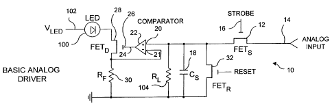
Figure 1 is a schematic of the basic LED driver
of the present invention.
Figure 2 is a schematic of the LED driver of the
present invention as configured to drive a single
pixel of a red/green/blue current-activated light
emitting device.
3


CA 02368386 2001-09-18
WO 99/48079 PCT/US99/05569
Figure 3 is a schematic of a 32 by 32 pixel
array of the LED drive of the present invention.
Figure 4 is a schematic of an 8 by 10 array of
the panels of Figure 3.
Figure 5 is a block diagram illustrating how a
red/green/blue signal and a sync computer output may
be combined with or substituted for an appropriate
video system.
Figure 6 is a block diagram of a shift.register
configuration of the present invention.
DETAILED DESCRIPTION OF THE PREFERRED EMBODIMENT
Referring now to the drawings in detail wherein
like numerals refer to like elements throughout the
several views, one sees that Figure 1 is a schematic
of analog LED driver 10. Driver 10 is applicable not
only to LEDs, but also to other display devices
wherein the intensity is controlled by the current.
The analog signal enters strobe FET (field effect
transistor) 12 via line 14. Strobe FET 12 is
activated by FET gate 16 during a specified strobe
period and the voltage is transferred to storage
capacitor 18 and presented to positive input 20 of
comparator 22. Output 24 of comparator 22 is
connected to gate 26 of drive FET 28 which turns on
passing current through LED 100 from its power source
102. The voltage developed on feedback resistor 30
is fed back to the negative input 21 of comparator 22
and reduces both output 24 and the current through
the LED 100 (and feedback resistor 30) until the
voltage across storage capacitor 18 is equal to the
voltage across feedback resistor 30 thereby resulting
in a drive current through LED 100 and feedback
resistor 30 which is stable at the selected value.
Additionally, a reset FET 32 is provided in parallel
with storage capacitor 18 to remove the charge upon
the storage capacitor 18 thereby blocking all current
4


CA 02368386 2001-09-18
WO 99/48079 PCT/US99/05569
from passing through LED 100. Additionally
illustrated in Figure 1 is leakage resistance 104
which represents the leakage resistance of the
comparator 22 and all other devices attached to the
positive input 20 of comparator 22. The value of
storage capacitor 18 is chosen so that it will hold
its charge within a specified tolerance until the
next strobe or reset pulse in view of the leakage
current through leakage resistance 104. If the input
voltage is in the range of 0.0 to 1.0 volts and the
desired current is 0 to 20 milliampr, feedback
resistance would be selected to be 50 ohms, for
example.
In the above configuration, the current in the
LED 100 can be varied continuously from zero to 20
milliampr, and not just limited to 256 steps.
The overall brightness of a display including a
plurality of LEDs 100 can be controlled by truncating
the display interval using the RESET command which
will not change the relationship between the various
colors and intensity.
Leakage resistance 104 can be selected by adding
a resistor (not shown) to have the resulting RC
constant (with the storage capacitor 18) emulate the
decay constant of video phosphors so that video image
will appear as they do on a video screen. This
cannot be done using conventional pulse width
modulation.
Very long persistence displays can be made by
using a one way pass transistor for the strobe FET 12
so that strobe FET will only add a voltage to the
storage capacitor 18, not subtract from it. The
reset pulse will reset the charge once per scan.
This is useful for very slow scan displays as in
radar systems.
Moving displays as for use as a stock ticker
display requires precise control over the display
5


CA 02368386 2004-O1-26
periods to insure undistorted movements. It is
possible to assign a gortian of the display for
moving tickers and control its display time using the
reset pulse while the balance of the screen may have
the variable persistence as required for a video
display.
Figure 2 is a typical arrangement of three basic
analog drivers 10R, 10~, lOH to drive a single pixel
of red/green/blue current activated light emitting
device 100. The three basic analog drivers lOR, 3.0~,
include elements corresponding to those shown in
Figure 1 but with the appropriate R, G or H (red,
green or blue) subscripts.
Figure 3 i.s a schematic of a 32 by 32 array of
pixels 100 are arranged on a basic panel 200 that
will be used as a building block to make very large
area displays. Panel 200 has the three light
emitting devices 1008, 100, 100H as color stripes
arranged on 0.2 inch pixel spacing to make, for
example a 6.4 inch by 6.4 inch basic panel 200. The
pixels and pixel spacing can be any size, but the 0.2
inch pixel spacing shown is the most convenient for
making wall sized displays for moderate sized rooms.
The red, green and blue inputs 14R, 14~, 14H are
presented to the entire array of 1024 pixels
simultaneously. Alternately,. in order to reduce
radiated noisy, the~video~signals can be gated with
the row enable signal so that_only one row will
receive the analog signals at a time. Row enable
selector 202 and column enable selector 204 are
provided so that only one set of three analog drivers
for one pixel are activated at one time. Each analog
video line is provided with 32 switches, one for each
row so that only one row of pixels are activated at
any one time. The row enable selector 202 is a
counter and a decoder which activates only one row at
a time. The counter is activated when the row enable
6


CA 02368386 2001-09-18
WO 99/48079 PCT/US99/05569
signal is active, and precesses on each row count .
After all 32 rows have been activated in sequence,
the outputs are turned off and the extend row enable
out signal is activated to turn on the next panel of
32 rows. A row counter reset signal is required to
reactivate the panel for reception of further data
signals. The column strobe counter and decoder are
activated one column at a time to strobe (or sample)
and store the analog value of the red, green and blue
video data into their respective analog drivers lOR,
10~, lOH, one pixel at a time in a manner similar to
the row enable system. When each of the 32 pixels in
a row have been activated and the data stored, the
extend column enable is made active to activate the
next panel so that it may store subsequent data in
the same row as the previous panel until the entire
row of video data has been stored in their drivers at
which time the row count is activated once and the
column strobe counters have been reset with a column
reset to prepare for the reception of the next row of
video data. The storage reset line is made available
to the entire panel but its use is not required for
general operation, only for special control purposes
as described hereinafter.
The analog drivers lOR, 10~, 10H, the control
counters and decoders 202, 204 and the video drivers
are intended to be built on a common substrate using
conventional TFT construction on glass, ceramic or a
metal substrate as desired with the light emitting
devices either deposited onto the analog drivers 10
using organic LED, polymer LED or other light
emitting devices that can be deposited, or by using
non-organic LEDs in chip form and installed on the
analog drive pads and wire bonded to the LED supply
voltage. The analog drivers may be made from
conventional packaged components or made on
conventional silicon substrates using conventional
7


CA 02368386 2001-09-18
WO 99/48079 PCT/US99/05569
CMOS construction processes.
Figure 4 illustrates an array of 8 rows by 10
columns of the panels 200 of Figure 3 thereby
resulting in a display 300 with a 320 by 256 pixel
array (each panel 200 being a 32 by 32 pixel array)
thereby resulting in a display face suitable for
emulating a CRT screen and displaying either an
output from a computer terminal or standard NTSC
video data. Any screen size can be assembled. The
red, green and blue analog video data is presented to
all panels simultaneously and selected for display as
described in Figure 3. Also shown in Figure 4 is the
interconnections of the row enable 204, column enable
202 and their extensions for panels 200 (A1_3, B1-3 and
Cl_3). One row of panels, 32 pixel rows, may have its
reset control wired to a control system to be shown
in Figure 5 which will allow it to have the precise
50/50 duty display cycle as required for smooth,
artifact-free scrolling data movement.
Figure 5 is a block diagram showing how either
a red/green/ blue and sync output from a computer 400
may be combined or substituted for a video system 500
that includes similar outputs. The video
distribution system 600 includes simple low impedance
buffers with unity gain to distribute the analog
video signals to the panels 200 as required. The
sync system 700 takes the combined horizontal and
vertical sync signals and generates the column count,
row count and reset signals required to coordinate
the distribution of the video data. The Store
Capacitor Reset signals are generated in this logic
as required for the special display function as may
be required.
Figure 6 is a analog shift register
configuration of panel 200' wherein full color image
can be moved down a display of essentially unlimited
length in a manner similar to the monochrome, single
8


CA 02368386 2001-09-18
WO 99/48079 PCT/US99/05569
intensity moving tickers as used for various stock
and commodity exchanges. The driver 10 is
substantially identical to that shown in Figure 1
with clock ~B functioning as a strobe, and an
interposing sample and hold stage has been provided
using as second strobe identified as ~A. When the
data is to be moved to an adjacent display, ~~, is
strobed to transfer the charge stored in the prior
analog drive 10 to a holding capacitor CA (or 18A).
Strobe ~p is deactivated and clock ~B activated to
transfer the charge to capacitor CB (or 18B). Thereby
data is moved from one pixel to the next and full
color images can be transferred through a practically
unlimited number of stages. Interposing buffers (not
shown) can be added from time to time with a gain
greater than one to compensate for intervening
losses, or one stage in each panel 200 can be
modified to provide a minor signal gain to make the
panel 200 have an overall gain of unity.
Thus the several aforementioned objects and
advantages are most effectively attained. Although
a single preferred embodiment of the invention has
been disclosed and described in detail herein, it
should be understood that this invention is in no
sense limited thereby and its scope is to be
determined by that of the appended claims.
9

Representative Drawing
A single figure which represents the drawing illustrating the invention.
Administrative Status

For a clearer understanding of the status of the application/patent presented on this page, the site Disclaimer , as well as the definitions for Patent , Administrative Status , Maintenance Fee  and Payment History  should be consulted.

Administrative Status

Title Date
Forecasted Issue Date 2004-08-17
(86) PCT Filing Date 1999-03-16
(87) PCT Publication Date 1999-09-23
(85) National Entry 2001-09-18
Examination Requested 2001-09-18
(45) Issued 2004-08-17
Deemed Expired 2007-03-16

Abandonment History

There is no abandonment history.

Payment History

Fee Type Anniversary Year Due Date Amount Paid Paid Date
Request for Examination $200.00 2001-09-18
Reinstatement of rights $200.00 2001-09-18
Application Fee $150.00 2001-09-18
Maintenance Fee - Application - New Act 2 2001-03-16 $50.00 2001-09-18
Maintenance Fee - Application - New Act 3 2002-03-18 $50.00 2002-03-06
Maintenance Fee - Application - New Act 4 2003-03-17 $50.00 2003-03-10
Maintenance Fee - Application - New Act 5 2004-03-16 $100.00 2004-01-13
Final Fee $150.00 2004-06-03
Back Payment of Fees $100.00 2005-03-21
Maintenance Fee - Patent - New Act 6 2005-03-16 $300.00 2005-03-21
Owners on Record

Note: Records showing the ownership history in alphabetical order.

Current Owners on Record
HOLLOMAN, CHARLES J.
Past Owners on Record
None
Past Owners that do not appear in the "Owners on Record" listing will appear in other documentation within the application.
Documents

To view selected files, please enter reCAPTCHA code :


To view images, click a link in the Document Description column. To download the documents, select one or more checkboxes in the first column and then click the "Download Selected in PDF format (Zip Archive)" or the "Download Selected as Single PDF" button.

List of published and non-published patent-specific documents on the CPD .

If you have any difficulty accessing content, you can call the Client Service Centre at 1-866-997-1936 or send them an e-mail at CIPO Client Service Centre.


Document
Description 
Date
(yyyy-mm-dd) 
Number of pages   Size of Image (KB) 
Representative Drawing 2002-03-06 1 6
Abstract 2001-09-18 1 50
Claims 2001-09-18 5 151
Drawings 2001-09-18 5 132
Description 2001-09-18 9 397
Cover Page 2002-03-07 1 40
Description 2004-01-26 9 399
Drawings 2004-01-26 5 131
Claims 2004-01-26 8 266
Representative Drawing 2004-07-15 1 6
Cover Page 2004-07-15 1 40
PCT 2001-09-18 6 263
Assignment 2001-09-18 4 139
Fees 2003-03-10 1 31
Prosecution-Amendment 2003-07-24 3 78
Prosecution-Amendment 2004-01-26 13 448
Fees 2002-03-06 1 34
Fees 2004-01-13 1 33
Correspondence 2004-06-03 1 31