Note: Descriptions are shown in the official language in which they were submitted.
CA 02370518 2001-10-12
WO 00/64010 PCT/US00/09283
TITLE: MEMORY MODULE WITH OFFSET NOTCHES FOR IMPROVED INSERTION AND
STABILITY AND MEMORY MODULE CONNECTOR
BACKGROUND OF THE INVENTION
Field of the Invention
This invention relates to memory modules for expanding memory capacity in
computer systems and to
memory module connectors.
2. Description of the Related Art
Both single in-line memory modules (SIMMs) and dual in-line memory modules
(DIMMs) and
corresponding memory module connector sockets for expanding memory with
computer systems are well known.
Generally speaking, in-line memory modules include a printed circuit board on
which a plurality of memory chips
such as DRAMS are surface mounted. A connective portion along one edge of the
printed circuit board is adapted
for insertion into a mating (i.e. accommodating) space of a connector. A
plurality of contact pads (also called
pins) on the connective portion mates with a plurality of corresponding
contacts inside the accommodating space
of the connector to provide for the transfer of electrical signals between the
memory module and the rest of the
computer system.
On a SIMM, the connective portion usually includes a plurality of contact pads
on either the front side of
the edge of the printed circuit board or on both the front and back sides of
the printed circuit board. In
configurations that include contact pads on both the front and back sides of a
SIMM, opposing contact pads on
the two sides are typically shorted together and therefore carrying the same
electrical signal. In a DIMM, the
contacts are positioned in the connective portion on both the front and back
sides of the printed circuit board. At
least some of the opposing contact pads on the two sides of the printed
circuit board of a DIIVIM are configured to
carry differing electrical signals, thereby increasing the signal density
without necessitating smaller contact pads
or a larger printed circuit board.
Figures 1A and 1B illustrate two embodiments of prior art DIMM memory modules
100 and 150,
respectively. Memory modules 100 and 150, as shown, include 84 contact pads,
such as contact pads 115A and
165A, on the front side, for 168 total contact pads. It is noted that the
number of contact pads may vary such that
memory modules with up to 200 contact pads are available on the market.
Memory modules 100 and 150 are configured to couple to appropriate memory
module connectors,
which are specifically designed to mate and secure the memory module. In
general, a connector comprises a
housing including an accommodating space, which is adapted to receive a
portion of the printed circuit board of
the memory module.
Turning to Fig. 1A in detail, memory module 100 includes a printed circuit
board 110. A region 103,
shown with dashed lines, for the placement of semiconductor integrated
circuits, such as DRAM memory chips or
other appropriate memory, occupies the majority of the space on a face of the
printed circuit board 110. The
contact pads 115 are disposed along one edge (i.e. the connective portion) of
the printed circuit board 110 from a
short distance from the left end to approximately the same distance from the
right end. The center of the length of
1
CA 02370518 2001-10-12
WO 00/64010 PCT/US00/09283
the printed circuit board 110 is marked with a centerline 101. A single notch
120 is positioned along the one edge
at substantially the center of the edge of the printed circuit board 110. In
other known embodiments, notch 120
may alternatively be positioned approximately one-half of the width of the
notch to either side of the center
location, as noted with dashed lines. Additional details regarding the notches
120 may be found with respect to
Fig. 1 C below. The printed circuit board 110 also includes indentions 105A
and 105B positioned on the left end
and right end, respectively. The indentations 105A and 105B are shaped to
receive module extractors, which may
be included as a part of the connector, to hold the memory module 100 in place
when the module extractors are in
a closed position.
Turning to Fig. 1B in detail, memory module 150 includes a printed circuit
board 160. The contact pads
115 are disposed along one edge of the printed circuit board 160. The center
of the length of the printed circuit
board 160 is marked with a centerline 151. A center notch 120A is positioned
along the one edge at substantially
the center of the edge of the printed circuit board 160. Memory module 150
also includes a left notch 120B
positioned to the left of center. Similar to the center notch 120A, the
location of the left notch 120B is also
known in other embodiments to be repositioned approximately one-half of the
width of the notch 120B to either
side of the illustrated location. The printed circuit board 160 also includes
indentions 105C and 105D positioned
on the left end and right end, respectively.
Fig. 1C is a close-up view of a notch 120. As shown, notch 120 is located on
the edge of the printed
circuit board 110 or 160 in a space along the row of contact pads 115. The
height of the notch 120 is just slightly
higher than the corresponding size of the contact pads 115.
It is noted that the notches 120 are configured to mate with keys in the
accommodating space in the
housing of the corresponding connector. A center key, which is configured to
mate with a center notch 120 or
120A, of the connector may be referred to as the "voltage key", while the left
key, which is configured to mate
with left notch 120B, may be referred to as the "functionality key". The names
refer to the different voltages
and/or functionalities that the three locations for each key (and therefore
notch) correspond, depending on the
manufacturer or standard.
One problem associated with the memory modules 100 and 150 is the difficulty
in correctly installing
the memory module 100 or 150 in the corresponding connector. Even with
installation guides as a part of the
connector, the memory module 100 or 150 may be installed backwards or
unevenly. While the use of a polarized
two-notch memory module, such as memory module 150, may decrease the
likelihood of installing the memory
module backwards, the notches 120A and 120B may not aid in installing the
memory module evenly. It may be
possible to install the memory module 150 with a slight tilt leading to one or
more misconnections or even shorts.
A related problem is the stability of the memory module 100 or 150 once
inserted in the corresponding connector.
Additional stabilizing features may inhibit simple and accurate insertion,
which may further lead to uneven
insertion and improper connections. Thus, it can be seen that an improved
memory module, connector, and
system thereof with improved ease of insertion and stability are desired.
SUMMARY OF THE INVENTION
The problems outlined above are in large part solved by an improved memory
module with offset
2
CA 02370518 2001-10-12
WO 00/64010 PCT/US00/09283
notches for improved insertion and stability and an improved memory module
connector configured to receive the
memory module. In one embodiment, the connector includes a first end, a second
end, and a center midway
between the first end and the second end. The connector housing further
includes an accommodating space for
receiving a connective portion of a printed circuit board of a memory module.
A first key and a second key are
disposed within the accommodating space of the housing. The first key is
positioned between the first end of the
housing and the center. The second key is positioned between the second end of
the housing and the center. A
distance between the first key and the second key is greater than 40% of the
length of the connector housing. In
one embodiment, one or more of the first key and the second key extend from
the accommodating space beyond a
top plane defined by a top side of accommodating space of the housing. The
distance between the keys may
advantageously allow for greater stability for a memory module coupled to the
connector without compromising
ease of insertion.
In another embodiment, a memory module is contemplated that includes a printed
circuit board
including a connective portion configured to be inserted into a memory module
connector. The connective
portion of the printed circuit board includes a first end, a second end, and a
center midway between the first end
1 S and the second end. A first notch and a second notch are positioned in the
connective portion of the printed
circuit board. The first notch is positioned between the first end of the
printed circuit board and the center. The
second notch is positioned between the second end of the printed circuit board
and the center. The distance
between the first notch and the second notch is greater than 40% of the length
of the printed circuit board. In one
embodiment, the first notch is farther from the first end of the printed
circuit board than from the center, and the
second notch is closer to the second end of the printed circuit board than to
the center. The distance between the
notches may advantageously allow for greater stability of the memory module
while coupled to a connector
socket without compromising ease of insertion.
BRIEF DESCRIPTION OF THE DRAWINGS
2S Other objects and advantages of the invention will become apparent upon
reading the following detailed
description and upon reference to the accompanying drawings in which:
Figs. 1A and 1B are side views of embodiments of memory modules in the prior
art;
Fig. 1C is a close-up view of a prior art notch;
Fig. 2A is an embodiment of a memory module including off set notches for
improved insertion into a
connector including off set keys;
Fig. 2B is a side view of the embodiment the memory module and connector of
Fig. 2A;
Fig. 2C is a close-up view of a notch shown in Fig. 2B;
Figs. 2D and 2E are a top view and a bottom view of the connector of Fig. 2B;
and
Fig. 3 is a three-dimensional cut-away view of a computer system including the
memory module of Fig.
3S 2A coupled to the connector of Fig. 2A.
While the invention is susceptible to various modifications and alternative
forms, specific embodiments
thereof are shown by way of example in the drawings and will herein be
described in detail. It should be
understood, however, that the drawings and detailed description thereto are
not intended to limit the invention to
3
CA 02370518 2001-10-12
WO 00/64010 PCT/US00/09283
the particular form disclosed, but on the contrary, the intention is to cover
all modifications, equivalents and
alternatives falling within the spirit and scope of the present invention as
defined by the appended claims.
DETAILED DESCRIPTION OF THE INVENTION
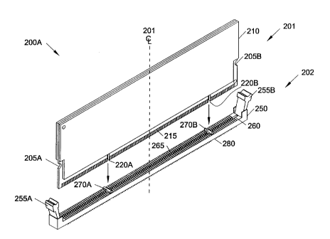
Turning to Fig. 2A, an embodiment of a memory module 201 including off set
notches 220 for improved
insertion into a connector 202 including off set keys 270 is shown in a three-
dimensional view 200A. The
memory module 201 includes a printed circuit board 210. The printed circuit
board 210 is shown as a multiple
layer composite printed circuit board including a region (refer to 202 in Fig.
2B) for one or more semiconductor
memory chips, such as DRAM. The center of the length of the printed circuit
board 210 is marked with a
centerline 201. The memory module 201 includes a first notch 220A positioned
along an edge of the printed
circuit board 210 between the first end (left as shown) of the printed circuit
board 210 and the center of the
printed circuit board 210. A second notch 220B is positioned along the same
edge of the printed circuit board
210 between a second end (right as shown) of the printed circuit board 210 and
the center of the printed circuit
board 210. The distance between the first notch and the second notch is
greater than 40% of the length of the
printed circuit board 210.
A plurality of contact pads 215 may also be included along the edge of the
printed circuit board 210 of
the memory module 201. As shown, the first and second notches 220A and 220B
divide the contact pads 215
into three groups. The first group is between the first edge of the printed
circuit board 210 and the first notch
220A. The second group is between the first notch 220A and the second notch
220B. The third group is between
the second notch 220B and the second edge of the printed circuit board 210.
Similar groupings of the contacts of
the connector 202 are discussed in detail with respect to Fig. 2D.
The memory module 201 may also includes indentations 205A and 205B located on
the ends of the
printed circuit board 210 of the memory module 201. The indentations 205A and
205B are each configured to
receive a corresponding portion of a module extractor of a connector, such as
module extractors 255 of connector
202.
In one embodiment, the first notch 220A is farther from the first end of the
printed circuit board 210 than
from the center, while the second notch 220B is closer to the second end of
said printed circuit board 210 than to
the center. In another embodiment, the plurality of contact pads 215 are
configured to abut a corresponding
plurality of contacts 265 in an accommodating space 260 of a connector, such
as connector 202, when the printed
circuit board 210 is received within the accommodating space 260.
Also shown in Fig. 2A is a connector 202 configured to receive a memory module
such as memory
module 201. The connector 202 includes a housing 250 with a length. The center
of the length is shown with the
centerline 201. The housing 250 includes a first end and a second end in a
fashion that parallels the printed
circuit board 210 of the memory module 201. The housing 250 further includes
an accommodating space 260,
which is adapted to accommodate a portion of a printed circuit board, such as
the printed circuit board 210 of the
memory module 201. A first key 270A is disposed within the accommodating space
of the housing 250,
positioned between the first end of the housing 250 and the center. A second
key 270B is also disposed within
4
CA 02370518 2001-10-12
WO 00/64010 PCT/US00/09283
the accommodating space of the housing 250 between the second end of the
housing 250 and the center. The
distance between the first key and the second key is greater than 40% of the
length of the housing 250.
The housing 250 of the connector 202 preferably also includes a plurality of
contacts 265 arranged
within the accommodating space 260. The contacts 265 are configured to abut a
corresponding plurality of
contact pads 215 on the printed circuit board 210 when the printed circuit
board 210 is partially received within
the accommodating space 260. The connector 202 also preferably includes two
module extractors 255A and 255
each coupled to an end of the housing 250. Each module extractor 255 is
rotationally operable to move between a
closed position (shown in Fig. 3) and an open position (shown in Figs. 2A and
2B). In the closed position, each
module extractor 255 is operable to "lock" in place at a corresponding
indentation, such as indentations 205 of
memory module 201. As shown, a plurality of solder connectors 280 may extend
from the bottom side of the
connector 202. The solder connectors 280 are operable to electrically couple
the connector 202 through a
mounting surface.
The memory module 201 is shown in Fig. 2A preparing to couple with connector
202, as shown by the
arrows between the notches 220 and the keys 270. When the coupling is
complete, the module extractors 255
will mate with the indentations 205 as the memory module 201 and the connector
202, mechanically and
electrically, securely "lock" into place.
In one embodiment, the housing 250 of the connector 202 includes a top side,
which defines a top plane
of the accommodating space 260. In this embodiment, one or more of the keys
270A and 270B key extend from
the accommodating space 260 beyond the top plane. One or more keys 270 may
extend beyond the top plane of
the accommodating space 260 by varying amounts. In a preferred embodiment,
both keys 270A and 270B extend
from the accommodating space 260 beyond the top plane by a distance of at
least 0.050 inches. In another
embodiment, the first key is farther from the first end of the housing 250
than from the center. In this
embodiment, the second key is closer to the second end of the housing 250 than
to the center.
In various embodiments, the number of contacts 265 within the accommodating
space 260 may vary,
above at least 200 contacts. In a preferred embodiment, the plurality of
contacts 265 includes 232 contacts. In
one embodiment, the plurality of contacts 265 is disposed within the
accommodating space 260 so as to be
vertically opposed to each other. When the portion of the printed circuit
board 210 is inserted into the
accommodating space 260, the printed circuit board 210 is weakly held between
the contacts 265. As the printed
circuit board 210 is pushed down to an implementation position, a tip of the
printed circuit board 210 elastically
deforms the contacts 265 so that the contact pads 215 of the printed circuit
board 210 and the contacts 265 are
brought into contact with each other as pressed by thus yielded elastic force.
A side view 200B of the memory module 201 and connector 202 is shown in Fig.
2B. The portion 203
of the memory module 201 operable to receive semiconductor chips is shaded.
The notches 220A and 220B, as
well as the contact pads 215, divided into three groups, are shown. The
indentations 205A and 205B are also
shown here. The center of the memory module 201 is again denoted by the
centerline 201. The connector 202 is
shown with the module extractors 255A and 255B on the ends and key270A and
270B on the top side extending
from the top plane (i.e. the upper edge in the side view) of the accommodating
space (not shown) of the connector
202. The area around the keys 270A and 270B is cut-away to show the keys 270.
The bottom side of the
5
CA 02370518 2001-10-12
WO 00/64010 PCT/US00/09283
connector 202 shows additional detail in this side view 200B. Besides a
plurality of solder connectors 280, a
plurality of placement posts 285 is also disposed on the housing 250 opposite
the accommodating space (i.e. the
bottom side). Each placement post 285 is configured to mate with a
corresponding hole in a mounting surface,
such as a circuit board.
In various embodiments, the location of the first and second notches 220A and
220B and the first and
second keys 270A and 270B may vary. It is contemplated that the first key 270A
may be located along the length
of the connector 202 between 15% and 35% of that length, as measured from the
first end, while the second key
270B may be located along that length between 65% and 85% of the length of the
connector 202, also measured
from the first end. It is likewise contemplated that the first notch 220A may
be located between 15% and 35% of
the length of the memory module 201, as measured from the first end of the
memory module, while the second
notch 220B may be located between 65% and 85% of the length of the memory
module 201, also measured from
the first end. In one embodiment, the distance between the first notch and the
second notch is greater than 50% of
the length of the memory module. In another embodiment, the distance between
the first key and the second key
is greater than 50% of the length of the connector.
In one contemplated embodiment, the first key is at least 1.525 inches from
the first end, and the second
key is at least 0.825 inches from the second end. In a preferred embodiment,
the first key is 0.061 inches in width
and located 1.900 inches from the first end. In this embodiment, the second
key is also 0.061 inches in width and
located 5.50 inches from the first end.
In various embodiments, the number and location of the placement posts may
vary. The illustrated
embodiment includes four placement posts. The two outer placement posts 285A
and 285D are each located
0.075 inches from the left and right ends, respectively. The two inner
placement posts 285B and 285C are shown
spaced 3.600 inches apart, corresponding to the locations of the first and
second keys 270A and 270B. It is
contemplated that the plurality of solder connectors 280 may be rearranged so
that the placement posts 285 may
be positioned as desired along the bottom side of the connector 202. In a
preferred embodiment, two placement
posts 285 are located at least 3.600 inches apart.
It is noted that in various embodiments, the dimensions of the memory module
201 may vary. The
overall length of the memory module 201 is preferably 6.400 t 0.005 inches.
The overall span of the plurality of
contact pads 215 is preferably 5.950 inches, with a space of 0.150 inches
allowed for each notch 220 position.
Each contact pad 215 is preferably spaced 0.050 inches typical. The height of
the memory module 201 is
preferably 2.000 inches with each indentation 205 positioned 0.700 inches from
the edge that includes the contact
pads 215. The depth of the memory module 201 has a preferred maximum of 0.290
inches. The portion of the
printed circuit board 210 of the memory module 201 that is intended to mate
with the connector 202 is preferably
0.175 inches minimum with a width of 0.050 t 0.004 inches.
Likewise, the dimensions of the connector 202 may also vary with each
embodiment. In a preferred
embodiment, the overall length of the housing 250 of the connector 202 is
6.914 inches, with 6.550 inches
between the centers of the two outer placement posts 285. The overall distance
covered by the solder connectors
280 is 5.95 inches, with 1.525 inches from the left end to the center of the
first key 270A and 0.825 inches from
the center of the second key 270B and the right end of the solder connectors
280.
6
CA 02370518 2001-10-12
WO 00/64010 PCT/US00/09283
Fig. 2C is a close-up view of a notch 220. Notch 220 is positioned in a space
in the plurality of contact
pads 215. Notch 220 is "taller" than the adjacent contact pads 215, having a
preferred height of 0.175 inches
minimum to a height of 0.100 inches for each contact pad 215. The preferred
width of each contact pad is 0.036
t 0.002 inches typical. The width of the notch 220 is preferably 0.071 t 0.004
inches, in contrast to the wider
notches typical in the prior art.
Figs. 2D and 2E are top and bottom views of the connector 202. In Fig. 2D, a
top view of the connector
202 is illustrated. The center of the connector 202 is marked by the
centerline 201. The accommodating space
260 is visible running down the center of the length of the connector 202. The
first key 270A and the second key
270B are shown in their respective spaces in the plurality of contacts 215.
There are two module extractors 255A
and 255B shown from the top at the ends of the connector 202. As shown, the
keys 270A and 270B are integral
components of a molding of the housing 250 of the connector 202, although an
embodiment where the keys 270A
and 270B are not integral components is also contemplated. The housing 250 may
be comprised of non-
conductive resin or plastic, as are well-known in the art.
In the embodiment illustrated, the plurality of contacts 215 are separated
into three groups by the keys
270A and 270B. The first group 291 of contacts 215 is located between the left
end of the connector 202 and the
first key 270A. The second group 292 of contacts 215 is located between the
first key 270A and the second key
270B. The third group 293 of contacts 215 is located between the second key
270B and the right end of the
connector 202. As illustrated, the first key is farther from the left end of
the housing 250 of the connector 202
than from the centerline 201. The second key is closer to the right end of the
housing 250 of the connector 202
than to the centerline 201.
In various embodiments, there may be differing numbers of contacts 215, and
the contacts 215 may be
separated by the keys 270A and 270B into groups with differing numbers of
contacts in each group 291, 292, and
293 of contacts 215. In one embodiment, the plurality of contacts includes at
least 200 contacts. In a preferred
embodiment, the plurality of contacts includes exactly 232 contacts. In
various embodiments, the first key is
located along the length of the housing 250 of the connector 202 between 15%
and 35% of the length of the
connector, as measured from the left end, and the second key is located along
the length of the housing 250 of the
connector between 65% and 85% of the length of the connector, also measured
from the first end.
In one embodiment, the number of contacts in the second group is larger than
the number of contacts in
either the first group or the second group. In a contemplated embodiment, the
number of contacts in the second
group is larger than the number of contacts in the first group and the second
group combined. In a preferred
embodiment, the first group includes at least 60 contacts, the second group
includes at least 140 contacts, and the
third group includes at least 32 contacts.
It is noted that as shown, the plurality of contacts 215 is disposed within
the accommodating space 260
so as to be vertically opposed to each other. A portion of a printed circuit
board 210, such as comprised in a
memory module 201, is weakly held between vertically opposed contacts in such
a state where the portion of the
printed circuit board 210 is inserted into the accommodating space 260, and as
the printed circuit board 210 is
pushed down to an implementation position, a tip of the printed circuit board
210 elastically deforms the contacts
265 so that the contact pads 215 of the printed circuit board and the contacts
265 are brought into contact with
7
CA 02370518 2001-10-12
WO 00/64010 PCT/US00/09283
each other. The printed circuit board 210 is held in place in the
accommodating space 260 by an elastic force
exerted by the deformed contacts 215.
In Fig. 2E, a bottom view of the connector 202 is illustrated. The centerline
201 denotes the center of
the connector 202 is this view also. The relative locations of the placement
posts 285 and the plurality of solder
connectors 280 are illustrated. The outer placement posts 285A and 285D are
positioned towards the ends of the
connector 202. The two inner placement posts 2858 and 285C are positioned in
the illustrated embodiment to
correspond to the top side spaces in the contacts 215 for the keys 270. The
diameters of the placement posts 285
are preferably 0.080 ~ 0.002 inches, except for the rightmost placement post
285D, which is 0.093 t 0.002 inches
in diameter.
The solder connectors 280 are shown in a preferred staggered configuration,
comprising four rows of
solder connectors 280. Neighboring rows of solder connectors 280 are
preferably separated by 0.075 inches, with
0.050 inches typical for the separation between solder connectors 280 as
measured along the length of the
connector 202. Each solder connector 280 is preferably 0.031 t 0.002 inches in
diameter. As shown, "pin 1" and
"pin 117" correspond to the leftmost solder connectors 280, pin 117 over pin
1. "Pin 116" and "pin 232"
correspond to the rightmost solder connectors 280, pin 232 over pin 116.
In Fig. 3, a portion of a computer system 300 is illustrated that includes a
circuit board 310, a connector
202 coupled to the circuit board 310, and a memory module 201 mated to the
connector 202. As shown, two
module extractors 255A and 2558 are coupled to respective ends of the housing
250 of the connector 202. Both
module extractors 255A and 2558 are in the locked position and positioned in
corresponding indentations of the
memory module. The edge portion of the memory module 201 is received within an
accommodating space of the
connector 202. The first key (shown previously) of the connector 202 is
positioned within the first notch (shown
previously) of the memory module 201. The second key of the connector 202 is
positioned within the second
notch of the memory module 201. The distance between the first key and the
second key is greater than 40% of
the length of the connector, and the distance between the first notch and the
second notch is greater than 40% of
the length of the memory module.
In various embodiments of the computer system 300, compatible embodiments of
the connector 202
and/or the memory module 201 described above may be incorporated in the
computer system 250. In one
preferred embodiment, the computer system further comprises one or more
semiconductor integrated circuits
coupled to the printed circuit board 210 of the memory module 201. One or more
of the semiconductor
integrated circuits includes a plurality of memory cells, which are
electrically coupled to various ones of the
plurality of contact pads.
In various embodiments, the housing 250 of the connector 202 may be comprised
of an electrically non-
conducting material. The electrically non-conducting material may be composed
of a resin or a plastic, or another
material, as desired. In other embodiments, the memory module may be comprised
of a composite including a
plurality of layers. The plurality of layers may include a plurality of layers
that are non-conducting. It is noted
that in some embodiments, the numbers and placement of features on the memory
module and/or the connector
may imply a corresponding number and/or placement of corresponding features on
the connector or memory
module. It is also noted that on stated measurements, where an uncertainty is
not expressly stated, an uncertainty
8
CA 02370518 2001-10-12
WO 00/64010 PCT/US00/09283
of 5 in the last decimal place is implied. Numerous other variations and
modifications will become apparent to
those skilled in the art once the above disclosure is fully appreciated. It is
intended that the following claims be
interpreted to embrace all such variations and modifications.
9