Note: Descriptions are shown in the official language in which they were submitted.
CA 02375442 2001-11-30
WO 00/73984 PCT/US00/15334
PROJECTIVE CAPACITIVE TOUCHSCREEN
TECHNICAL FIELD OF THE INVENTION
The present invention relates generally to touchscreens and, more
particularly, to a projective capacitive touchscreen suited for outdoor use.
BACKGROUND OF THE INVENTION
Touchscreens are well-established computer input devices. Uses of
touchscreens include point-of sale applications like cash registers at fast-
food restaurants,
point-of information applications such as department store information kiosks,
and
ticketing applications such as airline-ticket kiosks. As touchscreen
technologies mature,
the range of applications increases. To the extent that touchscreen technology
can
economically be made weather resistant and vandal resistant, the market for
touchscreens
will expand into outdoor and semi-outdoor applications.
Commercially available touchscreens utilize a variety of different touch
detection mechanisms. These detection mechanisms include interruption of
infrared (IR)
optical beams; electrical contact to a voltage gradient on a transparent
resistive coating via
flexing of a flexible coversheet; absorption of ultrasonic acoustic waves
propagating
along the touchscreen surface; capacitive shunting of an oscillating current
through either
a very thin or a thick dielectric layer to a user's finger and then through
the user's body to
ground; and detection of a touch on a touchscreen via force sensors supporting
the corners
of the screen.
To date, the touchscreen market has been dominated by resistive, acoustic,
and thin-dielectric capacitive touchscreens. For a variety of reasons,
however, it is
doubtful that any of these can fully meet the requirements imposed by an
outdoor
application. For example, the plastic coversheet used in a resistive
touchscreen is easily
vandalized by sharp objects (e.g., knives) or by burning (e.g., cigarettes).
Similarly,
shallow scratches on the surface of a thin-dielectric capacitive touchscreen
can lead to
CA 02375442 2001-11-30
WO 00/73984 PCT/LTS00/15334
2
unacceptable distortion in the measured touch coordinates thus making the
touch
detection mechanism susceptible to vandalism as well. Acoustic touchscreens
are
affected by water contaminants and therefore are typically not selected for
any application
in which the touchscreen may be directly or even indirectly exposed to rain
(e.g., water
dripping from wet clothes or an umbrella).
One type of touch detection mechanism that appears to be well suited for
outdoor applications is based on a thick-dielectric capacitive touchscreen.
Such systems
are often referred to as projective capacitive touchscreens since the
detection mechanism
involves projecting electric fields through a thick dielectric layer. This
type of
touchscreen is fundamentally insensitive to moisture, e.g., rain drops, on the
touch
surface. Additionally, the material comprising the exterior touch surface
plays no
fundamental role in the touch detection mechanism, thus providing design
flexibility. For
example, a replaceable, low-cost layer can be used as the exterior touch
surface.
In a typical projective capacitive sensor, three transparent substrates (e.g.,
glass) are laminated together, each substrate having a patterned transparent
resistive
coating. The patterned resistive coatings are fabricated from a material such
as ITO or
ATO. Silver frit traces are typically used to couple the patterned coatings to
the detection
electronics. In one configuration, the underside of the top substrate layer
has horizontal
Y-measuring electrodes while the top surface of the middle substrate glass has
vertical X-
measuring electrodes. The upper Y-measuring electrodes can be patterned in
such a way
as to minimize shielding of the underlying X-electrodes. The top surface of
the bottom
substrate layer contains a back guard electrode to isolate the sense
electrodes from the
electronic environment behind the touchscreen (i.e., display device). Thus in
this
configuration the X- and Y-electrodes are contained within separate planes.
In this type of projective capacitive sensor, the stray capacitive cross-
coupling between the X- and Y-measuring electrodes is inversely proportional
to the
distance between the X- and Y-electrode planes. Therefore reducing the gap
between the
X- and Y-electrode planes increases the capacitive cross-coupling, possibly
leading to an
increase in the demands placed on the associated electronics.
CA 02375442 2001-11-30
WO 00/73984 PCT/US00/15334
PCT application WO 95/27334 and U.S. Patent No. 5,844,506 disclose
another type of projective capacitive touchscreen utilizing fine wires of
between 10 and
25 micrometers thick as the electrodes. A variety of techniques are disclosed
for
electrically isolating the electrodes. For example in one configuration the
two sets of
S electrodes, i. e., the X- and Y-electrodes, are applied to opposite faces of
a thin dielectric
film. In another configuration the two sets of electrodes are applied to the
same side of
the dielectric substrate or film. Methods of electrically isolating the sets
of electrodes
include the deposition of an insulating layer between the two electrode sets,
the insulating
layer either being continuous over the entire touchscreen surface or applied
locally to the
intersections of the two electrode sets. In at least one of the disclosed
touchscreen
systems, the dielectric support substrate or film as well as the two sets of
electrodes are
encapsulated in a dielectric laminate, thereby eliminating the influence of
moisture as
well as providing a constant dielectric environment in the immediate proximity
of the
electrodes.
U.S. Patent No. 4,954,823, by the same inventor as PCT Application No.
WO 95/27334, discloses a touchscreen control system for use with projective
capacitive
touchscreens such as those disclosed in the PCT application. In the disclosed
control
system the electronics measure changes in sense-electrode capacitances due to
touches via
shifts in the frequency of a RC-time-constant controlled oscillator. A similar
technique
utilizing a RC-time-constant controlled oscillator for measuring the
capacitance changes
in a touch sensor is disclosed in U.S. Patent No. 4,103,252.
U.S. Patent No. 5,650,597 discloses a projective capacitive touchscreen in
which both the X- and Y-electrodes are formed in a single plane, the
electrodes arranged
as an array of horizontal sensor bars. A control circuit provides an
excitation signal to the
electrodes and receives a differential signal from the electrodes, the
differential sensing
signal providing touch position. In order to determine horizontal position,
the excitation
signal is provided to one side of the array and the sensing signal is received
on the other
side of the array. A similar array of unidirectional electrodes and a method
of obtaining
both X- and Y-coordinate information therefrom is disclosed in U.S. Patent No.
4,778,951. Projective capacitive touchscreen designs such as those disclosed
in U.S.
CA 02375442 2001-11-30
WO 00/73984 PCT/US00/15334
4
Patent Nos. 4,778,951 and 5,650,597 are dependent upon manufacturing processes
that
produce transparent conductive coatings of uniform resistivity that are
substantially free
of defects that can break the electrical continuity of the coating.
PCT Application No. WO 96/15464 discloses a controller for use with a
variety of touchscreen sensor array types. The signals from the array are
processed both
in the analog and digital domains, thus achieving reliable touch detection. In
one of the
disclosed signal processing techniques, the information from several sensor
areas is
interpolated to achieve fine positional resolution. The disclosed sensor
arrays include a
single surface array of pads that is substantially symmetrical, an
asymmetrical array of
pads (e.g., "Backgammon grid"), and dual orthogonal arrays arranged on
different
substrate layers.
A projective capacitive touchscreen using two sets of sensing electrodes
applied to a single substrate surface to accurately determine the X- and Y-
coordinates of a
touch is desired. The present invention provides such a system.
SUMMARY OF THE INVENTION
The present invention provides an improved touchscreen utilizing two sets
of electrodes fabricated in a single plane. The individual electrodes of each
set of
electrodes are formed from a continuous length of a conductive material such
as a fine
wire or a deposited conductive coating. The overall electrode pattern is such
that there is
no overlap of electrodes, thus not requiring insulating layers, coatings, etc.
between
electrodes.
In accordance with the invention, a variety of different electrode patterns
can be used. In one such electrode pattern, each electrode is comprised of a
loop of
conductive material, the loop substantially triangular in shape. The geometry
of adjacent
electrodes is reversed, i.e., positioning the base of the first triangularly
shaped electrode
adjacent to the apex of the next triangularly shaped electrode, etc. The
electrode width
and the electrode-to-electrode spacing determine the number of electrodes that
can be fit
within a given area. The number of electrodes affects both the complexities
associated
with the required electronics and the position determining algorithm as well
as the
CA 02375442 2001-11-30
WO 00/73984 PCT/US00/15334
achievable positional resolution. The positional resolution is also affected
by the shape of
the electrode edges, for example straight edges versus jagged edges.
In another electrode pattern according to the invention, each electrode is
comprised of a series of teeth, the shape and density of the teeth being
determined by such
5 factors as ease of manufacturing and desired positional resolution. By
varying the height
of the individual teeth, the general shape of each electrode is approximately
triangular.
The triangular shapes of the alternating electrodes are complementary such
that the base
of the first electrode is adjacent to the apex of the next electrode.
A touchscreen sensor using the sensing electrodes of the present invention
can use any of a variety of readout systems. For example, a frequency-domain
readout
approach can be used in which the operating frequency is fixed. In this
approach a touch
capacitance is detected by observing an impedance change at the operating
frequency,
typically by measuring a corresponding current change. Alternately changes in
a RC
decay time i can be measured, for example by observing frequency shifts in a
relaxation
oscillator. This technique is typically referred to as a time-domain approach.
In a third
alternate, capacitance changes can be detected via frequency shifts of LC
oscillators.
In order to determine touch position information using the electrodes of the
present invention, any of a number of techniques can be used. Preferably prior
to
determining touch position, a subset of the electrodes that are localized
around the touch
position is determined. Electrode localization reduces the effects of
background signals
while increasing the efficiency of the position determining algorithm. Once a
set of
localized electrodes has been determined the touch coordinates are calculated,
one
coordinate from the distribution of the touch signal within each set of
electrodes and the
other coordinate from the distribution of the touch signal between the two
sets of
electrodes.
A further understanding of the nature and advantages of the present
invention may be realized by reference to the remaining portions of the
specification and
the drawings.
CA 02375442 2001-11-30
WO 00/73984 PCT/US00/15334
6
BRIEF DESCRIPTION OF THE DRAWINGS
Fig. 1 is an illustration of a portion of one electrode array design according
to the present invention;
Fig. 2 is an illustration of a portion of an alternate electrode array design
according to the present invention;
Fig. 3 is an illustration of a portion of an alternate embodiment of an
electrode array design according to the present invention;
Fig. 4 is an illustration of an electrode interconnect design;
Fig. 5 illustrates a cross-section of one embodiment of the invention;
Fig. 6 illustrates a cross-section of an alternate embodiment of the
invention;
Fig. 7 is an illustration of a circuit equivalent to the electrode array
design
of the invention;
Fig. 8 is an illustration of a touchscreen using 17 triangularly shaped
1 S electrodes;
Fig. 9 is a schematic representation of the signal output from each of the
electrodes shown in Fig. 8;
Fig. 10 is an illustration of two electrodes similar to those shown in Fig. 1
with jagged, interlocking electrode edges;
Fig. 11 is an illustration of two electrodes similar to those shown in Fig. 2
with an increased number of teeth; and
Fig. 12 is an illustration of an electrode design that increases resolution
while decreasing the electronic channel count.
DESCRIPTION OF THE SPECIFIC EMBODIMENTS
Sensing Electrode Designs
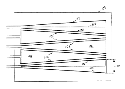
Figs. 1 and 2 illustrate portions of two different electrode array designs
according to the present invention. In Fig. l, electrodes 101-105 are formed
of individual,
continuous loops of a conductive material such that within a touchscreen
sensing area 107
electrodes 101-105 form a series of approximately triangular shapes in an
alternating
CA 02375442 2001-11-30
WO 00/73984 PCT/US00/15334
7
pattern. It should be understood that, unlike a pad-type electrode, the area
106 within
each triangularly shaped electrode is not conductive. The electrode
configuration shown
in Fig. 2 consists of a plurality of electrodes 201-205 each formed of a
continuous length
of conductive material. Each electrode 201-205 is comprised of a plurality of
teeth 206 of
varying height, the envelope of teeth 206 approximating a triangular shape. It
should be
understood that the shape of teeth 206 in Fig. 2 is only illustrative; other
teeth shapes can
be used with the present invention. It should also be understood that the
present invention
can utilize both electrode loops (e.g., electrodes 101-105) and non-loops
(e.g., electrodes
201-205). As in Fig. 1, electrodes 201-205 cover a touchscreen sensing area
207.
Electrodes 101-105 and 201-205 shown in Figs. 1 and 2, respectively, can
be fabricated from any conductive material. In the preferred embodiment the
electrodes
are fabricated from fine metal wires, preferably between 10 and 25 micrometers
thick.
Alternately, the electrodes can be fabricated from a deposited conductive
coating
patterned using a screen printing, photographic, or other process. If
sufficiently fine lines
are deposited, e.g., less than 25 micrometers in width, then the conductive
coatings need
not be transparent. If a transparent conductive coating such as ITO, ATO, or
fluorine-
doped tin oxide is used, then relatively wide line widths may be used. Fine
wire
electrodes are preferred due to the susceptibility of electrode line breaks in
transparent
conductive coatings. The electrodes are attached to a substrate 109 in Fig. l
and a
substrate 209 in Fig. 2. Substrates 109 and 209 can be of glass, a polymer
film such as a
PET, or other suitable material as is well known by those of skill in the art.
It should be understood that the electrode designs shown in Figs. 1 and 2
are merely illustrative, the inventors recognize that there are countless
minor variations of
these designs that can be used with the present invention. Many of the
possible variations
are given by the overall system requirements. For example, in order to achieve
greater
resolution, more electrodes can be fit within a given area. Additionally, the
slope of the
electrodes, the spacing between electrodes, the spacing between electrode
segments, etc.
can be changed to meet the system design requirements.
The electrode designs of the present invention provide many advantages
over prior electrode designs. First, since there is no overlap of individual
electrodes, all
CA 02375442 2001-11-30
WO 00/73984 PCT/US00/15334
8
of the electrodes can be formed on a single plane thus minimizing the number
of required
touchscreen substrates and lowering manufacturing costs. Second, as the
electrodes do
not overlap as noted above, the individual electrodes need not be insulated.
Therefore, if
fine wire electrodes are used, no insulating coating is required. Eliminating
the insulating
material further reduces visual obstruction from the electrodes.
Fig. 3 is an illustration of a portion of an alternate embodiment of an
electrode array that is similar to that shown in Fig. 1. In this design there
is a central
electrode region 301 in which portions of electrodes 303-306 are adjacent to
portions of
electrodes 309-312. Therefore in central region 301 there is enhanced X- and Y-
coordinate resolution while on either side of central region 301 there is only
limited Y-
coordinate information. This type of design is ideal for use in applications
in which it is
desirable to integrate a fully functional touchscreen (i.e., central portion)
with a side
touch-button input system.
There are a variety of methods that can be used to electrically connect the
1 S electrodes of the present invention with the touchscreen electronics. For
example, if fine
wire electrodes 401-413 are used as illustrated in Fig. 4, the fine wires can
provide
interconnect traces 415-427 to a connector 429. If the electrodes are
fabricated from a
transparent conductive coating such as ITO, interconnects 415-427 can be
fabricated from
silver-frit (e.g., on glass) or conductive-ink (e.g., on glass or polymer
film).
Another advantage of the present invention is that it allows the
interconnection between the sensing electrodes and the electronics to have a
much larger
impedance than is allowed in other touchscreen designs (e.g., resistive
touchscreens). In
the present system the impedance between the electrodes and the electronics
must be
smaller than the impedance of the stray capacitance from a sensing electrode
and an
adjacent sensing or guard electrode. For example, at an operating frequency of
30
kilohertz (i.e., kHz), a typical value of stray capacitance of 50 picofarads
(i.e., pF)
corresponds to an (imaginary) impedance of 1 /(2~fC) = 106 kilohms (i. e. ,
kSZ). Thus the
interconnect impedance must only be small compared to about 100 kS2. As a
result of this
requirement, the manufacturing options for interconnections are increased.
CA 02375442 2001-11-30
WO 00/73984 PCT/US00/15334
9
A variety of touchscreen cross-sections can be used with the present
invention. For example as illustrated in Fig. 5, a plurality of electrodes 501
are attached
to a substrate 503. Electrodes 501 are coupled to a connector 505 via
interconnects 507.
Connector 505 is then, in turn, coupled to touchscreen electronics 509 via a
flexible cable
511. A replaceable polymer (e.g., polycarbonate) touch surface 513 can be
mechanically
coupled to the electrode array, for example with an adhesive layer S 15,
making it difficult
to shatter the underlying glass substrate. Additionally, even if touch surface
S 13 is
damaged, for example by vandals, it can be easily replaced. Optionally, a
guard electrode
517 can be deposited on the bottom surface of substrate 503 to minimize the
effects of
stray capacitances between the sense electrodes and, for example, a display
device placed
behind the touchscreen. Also, as shown in Fig. 4, a perimeter guard electrode
431 can be
provided in the plane of the sense electrodes to minimize the effects of stray
capacitances
to objects around the perimeter of the touchscreen, e.g., metal associated
with the bezel
and its supporting structures.
In an alternate configuration shown in Fig. 6, a second substrate 601 is
bonded to the electrode assembly and lower substrate 503 with a safety-glass
adhesive
603. A safety-glass is the result of this lamination process.
Equivalent Circuit Analysis
In order to better understand the present invention, an equivalent circuit is
shown in Fig. 7. As illustrated, an electrode 701 with adjacent sensing
electrodes 702-
705 is capacitively shunted to a ground 707 by the touch of a finger (not
shown),
represented by a capacitor 709. In practice, a finger will capacitively couple
with
differing strengths to several neighboring sense electrodes. The distribution
of signals on
neighboring sense electrodes allows interpolation of the touch coordinate
perpendicular to
the long axes of the electrodes. For illustration purposes only, however, only
one touch
capacitance is included in Fig. 7.
The quantitative value of capacitor 709 is of the order of one pF. The
exact value depends on several factors including the size of the finger and
the thickness
and dielectric constant of the material between sense electrode 701 and the
finger. For
example, if the finger has an effective area, A, of one square centimeter
(i.e., 1 cm2) and
CA 02375442 2001-11-30
WO 00/73984 PCT/US00/15334
the material has a thickness, d, of three millimeters (i.e., 3 mm) and a
relative dielectric
constant of s/so=3, then capacitor 709 is equal to so * (s/Eo)*(A/d) _
(8.85pF/m)*3*(10~
m2)/(3*10-3 m) = 0.885pF. In order to support the touch reconstruction
algorithms,
preferably the electronics measure capacitance changes to a precision of about
two orders
5 of magnitude smaller than this, i.e., approximately t 0.01 pF.
Electrodes 701-705 are connected to an oscillating excitation voltage, V,
711. The frequency of operation may be, for example, 30 kHz. Current sensing
electronics 713 detects the current drawn by the electrodes when excited by
oscillating
voltage 711. Therefore if 711 produces 10 volts at 30 kHz and the capacitance
of
10 capacitor 709 is approximately 1 pF, then the touch results in a current
draw of:
DI = V*2~fC
= lOV*2~*30kHz*1pF or approximately 2 microamps (i.e., 2~.A). Such
current changes for each sense electrode may be measured and digitized. These
are the
signals processed by the touch algorithms.
A finger touch typically is not the only capacitance between a sensing
electrode and ground. The parasitic stray capacitance to ground is represented
by a
capacitor 715. This capacitance leads to a background current added to the
current I
measured at 713. In principle, this background current can be subtracted out
as an offset
in the touch algorithm. In practice, however, it simplifies the electronics
design if the
capacitance of capacitor 715 is not much larger than the capacitance 709 due
to a touch
and does not drift rapidly with time.
If desired, capacitance 715 can be greatly reduced by including guard
electrodes in the touchscreen assembly design. For example, a guard electrode
can be
placed between the plane of sensing electrodes and the display device as shown
in Figs. 5
and 6. Guard electrodes are driven with the same excitation voltage used to
excite the
sensing electrodes. By eliminating the voltage difference between the sensing
electrode
and the guard electrode, the shunt current through the stray capacitance to
the guard
electrode (i. e., capacitor 717 in Fig. 7) is approximately 0 (i. e. , AI =
AV* 2~f C = 0
because AV = 0). Thus the negative effects of the stray capacitance are
CA 02375442 2001-11-30
WO 00/73984 PCT/US00/15334
11
a I i m i n ate d w h a n AV / V < 1 % even if the stray capacitance 717
itself remains on the
order of 100 pF.
In an alternate embodiment, in addition to using the optional back guard
electrode, an optional perimeter guard electrode in the same plane as the
sensing
electrodes can be used. The capacitor labeled 717 in Fig. 7 represents the
total
capacitance from the sensing electrode to all guard electrodes.
There is also a stray capacitance between neighboring sense electrodes
indicated by capacitor 719. The numerical value of capacitance 719 varies
based on a
number of parameters including the width of the gap between neighboring
electrodes, the
length of the gap between neighboring electrodes, and the dielectric constant
of the
material surrounding the sensing electrodes. The stray capacitance between
neighboring
electrodes is approximately proportional to the natural log of the ratio of
the electrode
width to the electrode gap. A reasonable estimate for capacitance 719 is 40 pF
although
this value may easily vary by a factor of two depending upon the details of
the
touchscreen design. It should be understood that having a capacitance 719 that
is large
compared to capacitance 709 is not a problem since the neighboring sensing
electrodes
(i.e., electrodes 702-704) are driven by excitation voltage 711 and therefore
also function
as guard electrodes.
The last element in the equivalent circuit shown above is the interconnect
impedance 721. In some embodiments impedance 721 is approximately zero. Any
impedance, however, with a magnitude in the range of zero to approximately
1/(2~f C719)
is acceptable. C719 is the capacitance of element 719. Advantages of this
electronic
design freedom are noted below.
If the value of the interconnect impedance 721 becomes too large, then
there will be a tendency for the sensing electrode signal current to be
diverted via the
stray electrode capacitance 719 to neighboring sensing electrodes. This will
cause a
spreading or blurring of the touch signals as a function of sensing electrode
number.
These effects have been calculated with SPICE simulations. For example,
assuming an
operating frequency of 30 kHz, electrode stray capacitance 719 of 40 pF, guard
capacitance 717 of 20 pF, and interconnect impedance 721 corresponding to a
200 pF
CA 02375442 2001-11-30
WO 00/73984 PCT/US00/15334
12
capacitance, more than 75 percent of the current from a given sensing
electrode passes
through the corresponding current sensing circuit 713. If electrode stray
capacitance 719
is increased to 100 pF and if interconnect capacitance is reduced to 100 pF,
about 40
percent of the signal current remains in its nominal channel. In this case,
the signals may
still contain the desired touch information, but the quality of the signal
data is starting to
show significant degradation.
Therefore the range allowed for impedance 721 extends all the way up to
1/(2nf C~19). For typical values of C7I9 and f of 40 pF and 30 kHz,
respectively, 1/(2~f
C7i9) ~ 130 kS2. As a result, the design and manufacturing options for the
interconnections are greatly increased.
For clarity of presentation, the above analysis considered the case that the
touchscreen sensor will be read out with electronics using a fixed operating
frequency.
This technique is known as the frequency-domain readout approach. Touch
capacitance
709 is detected by observing an impedance change at the operating frequency,
typically
by measuring a corresponding current change. An alternate approach referred to
as the
time-domain technique measures changes in a RC decay time T, typically via
observation
of frequency shifts in a relaxation oscillator. The touch sensing electrodes
of this
invention may be used with either type of readout electronics. Therefore
although the
above analysis emphasizes the frequency-domain, the underlying sensor concepts
remain
the same.
Another technique that can be used with the projective capacitive sensors
of the present invention detects capacitance changes via frequency shifts of
LC
oscillators. The frequency of a LC oscillator is f = 2~/'~(LC). A change of
capacitance
OC leads to a frequency shift Of = -'/2 (OC/C).f.
Algorithm
A variety of algorithms can be applied to the signal data from the sensing
electrodes of the present invention to determine the X- and Y-coordinates of a
touch. A
few of these techniques are discussed briefly below although it should be
understood that
other techniques are equally applicable.
CA 02375442 2001-11-30
WO 00/73984 PCT/US00/15334
13
Fig. 8 is an illustration of a touchscreen using 17 triangularly shaped
electrodes 801-817 such as those discussed with reference to Figs. 1 and 4. As
in the
previous illustrations, the elongated axis of each electrode is parallel to
the X-axis
although it should be understood that the touchscreen could be designed with
the
elongated axis parallel to the Y-axis or using a different electrode design
(e.g., see Fig. 2).
Circle 819 represents the location of contact between touch surface 800 and
the tip of the
user's index finger. A screen touch at location 819 will couple most strongly
to electrode
808, but will also induce signals of varying strengths on electrodes 809 and
807 and
perhaps electrodes 806 and 810. The narrower the width of the electrode and
the greater
the thickness of material projected through (i.e., exterior touch surface),
the greater will
be the number of electrodes responding to the finger touch.
Ellipses 821 and 823 represent the palm of the user's hand. The palm is
assumed to be above, but not in contact with, the touch surface. Ellipse 821
represents
the palm of a right-handed user while ellipse 823 represents the palm of a
left-handed
user. There may be some parasitic capacitive coupling between the palm and the
underlying electrodes. As shown in Fig. 8, electrodes 803-807 may be subject
to
background signals due to the palm of the user's hand.
Methods for obtaining an output signal from each of the electrodes and, if
desired, compensating for gain variations between electronic channels, are
well known by
those of skill in the art and will therefore not be discussed in detail
herein. Assuming an
output signal from each electrode, there are numerous touch reconstruction
algorithms
that can be applied to the touchscreen system of the present invention. A few
representative examples are provided below although it is understood that
these examples
are not exhaustive and that there are other touch reconstruction algorithms
that are equally
applicable to the invention.
The first step of most touch reconstruction algorithms is simply
determining that a touch has occurred. One of the simplest approaches to
detecting a
touch is based on an electrode output signal exceeding a signal level
threshold. Fig. 9 is a
schematic representation of the signal output from each of the electrodes
shown in Fig. 8.
As shown, only the signal from electrode 808 exceeds threshold level 901.
CA 02375442 2001-11-30
WO 00/73984 PCT/US00/15334
14
A problem with the simple threshold level approach illustrated in Fig. 9
can occur if the touch area is small compared to the electrodes and centered
between two
electrodes. In this situation the signal will be split between the two
electrodes, possibly
leading to insufficient signal in either electrode to surpass the threshold
level. To
overcome this problem the touch detection algorithm can be modified such that
touch
detection occurs whenever the sum of the signal levels from two adjacent
electrodes
exceeds a given threshold level. Similarly, the algorithm can be modified such
that touch
detection occurs whenever the sum of the signals from a predetermined number
of
adjacent electrodes (i.e., 3, 4, ..., all electrodes) exceeds a threshold
level. A benefit of
detecting touch with a small number of electrodes rather than a large number
of electrodes
is in palm rejection (i.e., minimizing false touch detection based on a large
number of
electrodes each outputting a small signal due to the proximity of a large
object near the
touchscreen). This technique of avoiding false touches is particularly
effective if the long
axes of the electrodes are horizontal, as shown in Fig. 8, rather than
vertical.
After a touch has been detected using a technique like those described
above, preferably the touch is localized. In this step a subset of all of the
sensing
electrodes is identified, the subset consisting of those sensing electrodes
that are near the
touch position. There are several benefits to this optional step. First, by
limiting the
number of electrodes the position determining algorithm can operate more
efficiently and
therefore faster. Second, the effects of palm-induced background signals and
random
electronic noise are reduced.
There are several ways to localize the touch. One way is to identify the
neighboring pair of electrodes with the largest combined signal. Preferably an
additional
electrode on either side of the selected pair is added to the set of
electrodes, resulting in a
set of four electrodes that can be used to compute the X- and Y-coordinates of
the touch.
It is understood that greater numbers of electrodes can be included in the
localized set of
electrodes without departing from the invention.
Referring to Fig. 8 and assuming the number of localized electrodes is
limited to four, the local group of sensing electrodes can be divided into a
pair of odd-
numbered or right-biased electrodes and a pair even-numbered or left-biased
electrodes.
CA 02375442 2001-11-30
WO 00/73984 PCT/US00/15334
The division of signal between these two pairs of electrodes provides an X
coordinate
measurement. For touch 819 of touchscreen 800, the left and right signal sums
can be
defined as follows:
L = Ssos + Ssio
R = Sso9 + Sso7
The X coordinate, Xt, of the touch is given by:
Xt = L/(L+R)
This measured coordinate, X~, can be easily offset and scaled as needed to
10 match the coordinate system of the display device. For example:
XDisplay = (Magnification)( X~ + Offset
The Y-coordinate of the touch can be calculated by a weighted sum. For
example, if Y~ are defined as the Y-coordinates of the centerlines of the
sensing
electrodes, the value of the touch Y-coordinate, Yt, can be estimated from:
15 Y = (L* Sgo9* Yso9 + R * Ssos * Ysos + L * Sgo~ * Yso~ + R * Ssio * Ysio)/
(2L*R)
Alternately, Yt may be determined by fitting a curve to the weighted
signals L*Sso9, R*Ssos, L*Sso~, and R*Ss~o. The left and right signal sums R
and L are
used here to correct for the biases in the electrode signals as a function of
the X-
coordinate. More sophisticated weighting and curve fitting schemes can also be
used,
including schemes in which corrections are made to the X-coordinate based on
the Y
value and vice versa.
As with some other touch technologies (e.g., acoustic, force, capacitive)
the sensors of the present invention can provide a value, Z, corresponding to
the strength
of the touch. For example Z may simply be the sum of the signals for the local
group of
sensing electrodes, i. e., Sso7 + Ssos + Sso9 + Sslo
The Z-coordinate can be used by the application software to dynamically
adjust the touch threshold. Typically, the first interaction between a touch
based kiosk
and a new user is a touch by the user to 'wake up' a menu system. Often waking
up the
menu system also causes the kiosk to stop displaying either an attention
getting image or
some form of advertisement. For the first touch, it may be appropriate for the
application
CA 02375442 2001-11-30
WO 00/73984 PCT/US00/15334
16
to accept a touch that is based on a low Z threshold value since there would
be little harm
caused by the occasional false touch. During the initial touch the application
software
will see a stream of Z values. Preferably the system determines the maximum Z
value
during this initial touch and, based on the value of this maximum Z value,
sets a second
touch level threshold. For example, the second level could be set at some
percentage
(e.g., 50%) of the maximum Z value. Thus the Z value can be used to adapt to
differences
in finger sizes, the difference between gloved and ungloved fingers, etc.
Once the X- and Y-coordinates, and optionally the Z-coordinate, are
calculated, the algorithm outputs the coordinates to the operating system.
In a variation of the above algorithm, odd and even numbered sensing
electrodes are paired, thus effectively providing a bar electrode of constant
width as a
function of X (or Y, depending upon the orientation of the long axis of the
electrodes).
Thus in Fig. 8, electrodes 801 and 802 are paired, electrodes 803 and 804 are
paired, etc.
Alternately, electrodes 802 and 803 are paired, electrodes 804 and 805 are
paired, etc.
1 S Based on these two pairing schemes, two tilted Y-coordinates can be
calculated where
each of the calculated Y-coordinates is determined from the average of the Y
signal
values.
Thus in the above example, Y~ is determined from the electrode-pair signal
amplitudes (Sgo~ + Ssos) ~d (Sso9 + Ssio) while Y2 is determined from the
electrode-pair
signal amplitudes (Sgo6 + Sso~) and (Ssos + Sso9), yielding:
YW((Sso7 + Ssos)*~Yso~ + Ysos)/2 + (Sso9 + Ssio)*(Yso9 + Ysio)/2)/(Sso7 + Ssos
+ Ssos +
Ssio)
YZ=((Sso6 + Sso7)*(Ysos + Yso7)/2 + (Ssos + Sso9)*(Ysos + Yso9)/2)/(Ssob +
Sso7 + Ssos +
Sso9)
Either weighted averages or curve-fits can be used. Since the bar electrodes
formed by
the pairs of electrodes in Fig. 8 are not absolutely horizontal, and since the
tilt of even-
odd pairs is the opposite of the tilt of odd-even pairs, Y~ and Y2 will
deviate with opposite
signs from the touch Y-coordinate by an amount proportional to the X-
coordinate
(assuming that X = 0 is at the center of the touch region). Therefore
averaging Y1 and YZ
will give the touch Y-coordinate (i.e., Yt = (Y~ + Y2)/2).
CA 02375442 2001-11-30
WO 00/73984 PCT/US00/15334
17
Furthermore, the orthogonal or X-coordinate can be calculated from the
difference of these values. Such algorithms are somewhat analogous to depth
perception
in binocular vision. Preferably the X-coordinate is calculated according to
the equation:
X=A(Y~-Y2)+B
where A and B are constants that provide the desired scaling and offset. The
area under
the finger-touch peak in either signal-pair provides a Z value.
It should be understood that the touch algorithms described above are only
meant as examples illustrating how both the X- and Y-coordinates can be
determined
from the sensing electrodes of the present invention. Various other touch
algorithms may
also be used with the touchscreens of this invention
Electrode Design
There are a variety of electrode parameters that can be varied depending
upon the overall system requirements. For example, the width of the individual
electrodes (see width 111 in Fig. 1 or width 211 in Fig. 2) directly impacts
the system
complexity as a touchscreen using wider electrodes requires fewer electrodes,
and thus
fewer interconnects, electronic channels, etc. However, wider and thus fewer
electrodes
typically results in positional information being lost. To some extent this
problem can be
minimized by channel multiplexing, i.e., coupling more than one electrode to
each
channel.
Another parameter that can be varied to provide higher positional
resolution is the shape of the electrodes. For example, instead of having a
smooth outline
as shown in Fig. 1, the edge of the electrodes can be made up of a series of
interlocking
'teeth' as shown in Fig. 10. Similarly, the number of teeth in the electrodes
shown in Fig.
2 can be increased as shown in Fig. 11.
Fig. 12 is an illustration of a portion of an electrode design that
incorporates electrodes shaped to achieve high resolution with an electronics
design that
reduces the number of required electronic channels. As shown, electrodes 1201-
1204 are
coupled to the touchscreen electronics on one side of the touchscreen while
electrodes
1205-1207 are coupled on the second touchscreen side. It should be understood,
CA 02375442 2001-11-30
WO 00/73984 PCT/US00/15334
18
however, that all of the electrodes can be coupled to the system electronics
on one side, as
shown in Fig. 4.
In the illustrated reduced electronic channels scheme, electrode 1201 is
connected to electronics channel 1209 via an interconnect with a capacitance
C~.
Similarly, electrode 1203 is connected to electronics channel 1211 via an
interconnect
with a capacitance CI. In contrast, electrode 1202 is connected to both
electronic channels
1209 and 1211 via interconnect capacitances of CI/2. As a touch is moved from
electrode
1201 to electrode 1203, the signal amplitudes will shift smoothly from channel
1209 to
channel 1211. Note that the signal from electrode 1202 is split evenly between
electronic
channels 1209 and 1211. In this configuration, the fact that the present
invention tolerates
an interconnect impedance 721 (as previously described) is a great advantage.
It should
be understood that electrodes 1205-1207, and for this example electrodes 1205
and 1206,
offer further smoothing of a touch moving from electrode 1201 to 1203.
As will be understood by those familiar with the art, the present invention
may be embodied in other specific forms without departing from the spirit or
essential
characteristics thereof. Accordingly, the disclosures and descriptions herein
are intended
to be illustrative, but not limiting, of the scope of the invention which is
set forth in the
following claims.