Note: Descriptions are shown in the official language in which they were submitted.
CA 02375749 2001-11-28
WO 01/76129 PCT/USO1/09714
-1-
SCALABLE CRYPTOGRAPHIC ENGINE
Background of the Invention
Field of the Invention
The present invention relates generally to data encryption systems, and more
particularly to a cryptographic engine that has scalable processing
capabilities and
that is for use in communications devices requiring secure transmission and
reception of data.
Description of Related Art
As the sophistication and importance of broadband communications devices
continues to increase in both in commercial and military applications, so does
the
need to maintain the security of data transmitted by these devices. Currently,
such
broadband communications devices include cryptographic coprocessors for
executing encryption and decryption processing algorithms, while a general-
purpose controller typically executes more traditional device processing
algorithms.
While conventional encryption/decryption engine architectures enable data to
be securely transmitted across the bandwidth, such architectures do have
associated limitations. For example, in a multi-band multi-mode radio or other
similar device requiring high performance cryptographic processing, the
underlying
cryptographic engine architecture must include several cryptographic co-
processors
to handle the symmetric encryption and decryption algorithm processing
required
for secure data transmission and reception. Because the engine footprint must
be
large enough to accommodate the coprocessors, an engine design including
several cryptographic coprocessors tends to increase overall manufacturing
costs
and limit device design possibilities, as well as increase overall chip power
requirements.
CA 02375749 2001-11-28
WO 01/76129 PCT/USO1/09714
-2-
Brief Description of the Drawings
Additional objects and advantages of the present invention will be more
readily
apparent from the following detailed description of preferred embodiments
thereof
when taken together with the accompanying drawings in which:
FIG. 1 is a schematic block diagram of a programmable cryptographic engine
according to a first preferred embodiment of the present invention;
FIG. 2 is a schematic block diagram of the main processor shown in FIG. 1;
FIG. 3 is a schematic block diagram of one of the coprocessor slices shown in
FIG. 1;
FIG. 4 is a diagram of a coprocessor permuter shown in FIG. 3;
FIG. 5 is a diagram of a non-linear function section of the permuter shown in
FIG. 3;
FIG. 6 is a diagram of a linear logic unit of the coprocessor shown in FIG. 3;
FIG. 7 is a schematic block diagram of the coprocessor controller shown in
FIG. 1;
FIG. 8 is an instruction format for the coprocessor microsequencer shown in
FIG. 1;
FIG. 9 is a schematic block diagram of a programmable cryptographic engine
according to a second preferred embodiment of the present invention;
FIG. 10 is a schematic block diagram of a programmable cryptographic engine
according to a third preferred embodiment of the present invention;
FIG. 11 is a schematic block diagram of a programmable cryptographic engine
according to a fourth preferred embodiment of the present invention; and
FIG. 12 is a schematic block diagram of a programmable cryptographic
engine according to a fifth preferred embodiment of the present invention.
Detailed Description of a Preferred Embodiment
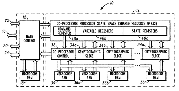
Referring now to the drawings in which like numerals reference like parts,
FIG.
1 shows a cryptographic processor engine 10 according to a first embodiment of
the present invention. The engine 10, which is typically fabricated on a
single
semiconductor substrate, includes a main processor 12 for performing general
CA 02375749 2001-11-28
WO 01/76129 PCT/USO1/09714
-3-
purpose engine processing, and a coprocessor 14 having a scalable
cryptographic
processing capacity that will be described below in more detail. The engine 10
is
capable of processing externally-received data packets via any of a variety of
techniques including plain-text data encryption, cipher-text data decryption,
in-band
signaling processing required for bit, word or frame formatting, in-band
signal
detection, and error detection and correction processing techniques. The
engine
is capable of executing a single or multiple independent cryptographic
algorithms on a large state space, and is capable of supporting both active
and
shadow techniques, thereby enabling algorithm and key agility through rapid
10 context switching between algorithms and/or state and variable
associations.
As shown in FIG. 1, the main processor 12 handles all communications with
external devices, such as other communications device processors, through
several
interfaces. Specifically, the main processor 12 receives configuration and
initial
state loading instructions through a control interface 16 and performs
processing
operations, such as asymmetric processing operations used to initialize a
data/voice link, based on instructions stored in and fetched from a processor
memory 18, such as a microcode RAM, in response to the received configuration
and initial state loading instructions. The main processor 12 may also receive
data
to be processed from an external memory such as a RAM memory (not shown) via
a RAM interface 20 if a particular application requires temporary storage of
data to
be processed, and outputs the data after it has been processed on one or both
of
the red and black interfaces 22, 24.
Referring to FIG. 2, the main processor 12 includes a 32-bit microsequencer
26 that includes the interfaces 16, 20, 22, 24. Also, the microsequencer 26 is
coupled to an arithmetic logic unit (ALU) 28, multiplexers 29a, 29b, a
register file 30
and a comparison unit 34. The microsequencer 26 manages all main processor
resources based on instructions stored and fetched from the microcode RAM 18.
The ALU 28 is programmed to perform operations such as AND/OR, XOR,
ADD and SUBTRACT operations to enable the main processor 12 to perform
standard Boolean and arithmetic processing of data packet portions, referred
to as
data packet elements, selectively output from the multiplexers 29a, 29b. The
data
packet elements processed by the ALU 28 are output to either the register file
30,
CA 02375749 2001-11-28
WO 01/76129 PCT/USO1/09714
-4-
to the microsequencer 26 for transmission back to external processors through
either the red or black interfaces 22, 24, or to the comparison unit 34. The
register
file 30 functions as a scratchpad memory for temporary data storage when a
message received from the microsequencer 26, such as a decode message,
requires that the ALU 28 run an algorithm several times, while the comparison
unit
34 enables the main processor 12 to compare two 32-bit data packet elements
output from the microsequencer 26 and to generate the number of bit errors
occurring in one clock cycle for engine processing integrity purposes.
Referring back to FIG. 1, the scalable coprocessor 14 is controlled by the
main
processor 12 and performs cryptographic processing functions in parallel with
the
functions performed by the main processor. The coprocessor is operative. The
coprocessor is a multiple slice coprocessor with cryptographic processing
slices
34a-34n each having corresponding volatile memories, such as microcode RAMs
36a-36n, for storing slice-specific independent control instructions, where
the
number n is application-specific and is based on design parameters such as
chip
cost and performance requirements. A coprocessor controller 38 sequentially
handles all operations to be performed by the coprocessor based on
instructions
retrieved from the memory 39 in response to commands received from the main
processor 12, and informs the main processor 12 each time a slice has
completed a
specific processing operation.
Because the slices 34a-34n perform cryptographic processing operations
independently from one another and in parallel with the processing of the main
processor, the coprocessor 14 is capable of simultaneously performing several
independent cryptographic processing operations, with the exact number of
possible operations being dependent on the number of slices, at higher, albeit
synchronous, clock rates than that of the main processor 12. For example, the
coprocessor may receive instructions to loop through a particular encryption
algorithm 64 times to generate encrypted data packets, while the main
processor
need only input the data packets to be encrypted to the coprocessor 14 and
subsequently output the resulting encrypted data packets through the red/black
interfaces 22, 24. Therefore, the cryptographic processor engine of the
present
CA 02375749 2001-11-28
WO 01/76129 PCT/USO1/09714
-5-
invention is capable of supporting data rates equal to the throughput of the
coprocessor 14 in a manner that minimizes overall engine power consumption.
As shown in FIG. 1, the coprocessor includes a 64 x 32-bit register bank 40
that includes a command register 40a, variable registers 40b and state
registers
40c. The command register 40a, hereinafter referred to as the register R0, is
for
receiving and loading commands from the main processor 12 and for subsequently
sending those commands to the coprocessor controller 38. The variable
registers
40b are for storing data packet variables for the slices 34a - 34n such as,
for
example, a session key for use by the coprocessor 14 in performing
cryptographic
functions. The state registers 40c are for storing state data such as, for
example,
channel program data representing a current execution state for an encryption
algorithm being executed by one of the slices. The state registers 40c, which
are
typically accessible by main processors in conventional cryptographic engine
architectures, are included as part of the coprocessor 14 in the present
invention to
enable the number of coprocessor slices to be set according to cryptographic
application processing parameters.
FIG. 3 is a block diagram of the cryptographic slice 34a of FIG. 1, with it
being
understood that the other cryptographic slices 34b - 34n are of like structure
and
similar function, with the exact function of each slice being dependent on the
instructions stored in the microcode RAMs 36a - 36n. The cryptographic slice
34a
performs a designated encryption/decryption function for the cryptographic
engine
10 that can be independent from processing functions performed by other
cryptographic slices that may be included in the engine architecture, even
though
the slice 34a may share state space in the register bank 40 with other slices.
The
slice 34a includes an 8-bit microsequencer 50 that provides the slice with
processing power and that manages program flow for the slice based on
instructions stored in and fetched from the microcode RAM 36a. Because each
slice includes a microsequencer such as the microsequencer 50, each slice is
capable of performing a processing function independently from other slices.
The
independent processing capability of each slice produces economies of scale,
as
the coprocessor can simultaneously execute a number of independent
CA 02375749 2001-11-28
WO 01/76129 PCT/USO1/09714
-6-
cryptographic algorithms corresponding generally to the number of coprocessor
slices, thereby increasing overall engine data packet throughput.
The microsequencer 50 controls operation of an input register 54, which in
turn provides control bits necessary to move data into and out of the register
bank
40 and control bits necessary to select various coprocessor cryptographic
functions.
More specifically, the microsequencer 50 initiates operation of the input
register 54
by inputting an address into an input register non-volatile memory 56, such as
a
microcode RAM, that stores register-specific operating instructions. The
microsequencer 50 then latches data output from the RAM 56 to control a
permuter
58, which has a 160 x 160-bit linear permutation section 60 and a non-linear
function unit including a 160 x 144-bit permutation section 62 and a non-
linear
lookup table section 64 with, for example, sixteen 9:1 lookup tables.
In operation, the data slice 34a is capable of processing ten 32-bit data
packet
elements input from the register bank 40 to produce four 32-bit
encrypted/decrypted
data packet elements for return to the state registers 40c every clock cycle.
More
specifically, five of the input data packet elements, indicated at 70, are
input into
and permuted by the linear permutation section 60 to create four new 32-bit
data
packet elements at 72 that are then input into the linear function unit 66.
The other
five input data packet elements, indicated at 74, are set up by the nonlinear
permutation section 62 before being mapped to values in the lookup tables 64
and
then output to the linear logic unit 66.
In FIG. 4, the linear permutation section 60 is shown in more detail. The
linear
permutation section 60 is capable of routing any input bit to any output bit
based on
control instructions stored in a local section memory (not shown). Each of the
five
32-bit data packet elements at 70 is input into a 4:1 multiplexer 76. The
multiplexer
76 outputs each 32-bit data packet element as four separate 8-bit data packet
elements. The 8-bit data packet elements in turn are input into an 8:1
multiplexer
78. The multiplexer 78 outputs each of the 8-bit data packet elements to a
multiplexer 80 as eight separate bits of data. The multiplexer 80 sends each
of the
data bits along with the thirty-one other 1-bit outputs as a permuted 32-bit
output to
the linear logic unit 66.
CA 02375749 2001-11-28
WO 01/76129 PCT/USO1/09714
FIG. 5 shows that the non-linear lookup table section 64 is composed of
sixteen separate 512 x 1-bit lookup tables, as indicated generally at 81.
Sixteen 9-
bit data packet elements, resulting from the five 32-bit data packet elements
at 74
being permuted by the non-linear permutation section 62, are input into
corresponding ones of the lookup tables and mapped to a single bit non-linear
table
value. The resulting 16-bit data packet element is concatenated at 80 with a
previously-generated 16-bit result stored in a delay register 82 to form a
fifth new
32-bit data packet element input to the linear function unit at 84.
Still referring to FIG. 5, the non-linear function unit configuration of the
present
invention enables different slice encryption/decryption algorithms to
efficiently utilize
the non-linear function unit lookup tables 81. For example, one algorithm may
utilize four of the memories as a 4-bit lookup table, while a separate
algorithm may
simultaneously and independently address eight of the other memories for use
as
an 8-bit lookup table. Any combination of the lookup tables 81 may be utilized
to
create a single multi-bit lookup table based on the cryptographic algorithm
parameters necessary for a particular slice to perform its stored
cryptographic
algorithm or function.
Referring now to FIG. 6, the linear function unit 66 is shown in more detail.
The linear function unit processes the four 32-bit input data packet elements
72
generated by the permutation section 60 and the one 32-bit data packet element
84
generated by the non-linear function unit to produce the four 32-bit linear
results at
86. More specifically, the linear function unit 66 either processes the data
packet
elements In1 - In5 through the EXOR tree indicated generally at 90 or bypasses
data packet elements In1 - In4 directly to a multiplexer bank 92 based on
instructions from the microsequencer 50. The multiplexer bank 92 then outputs
the
resulting data packet elements as data packet elements Out1 - Out4 back to the
register bank 40 for transmission back to the main processor 12.
Referring to FIG. 7, a block diagram of the coprocessor controller 38 is
shown.
The coprocessor controller 38 includes an 8-bit microsequencer 94 that
provides
slice processing power and that manages program flow for a given slice-
executed
encryption/decryption algorithm in response to commands received from the main
processor 12. The microsequencer 94 according to one embodiment of the present
CA 02375749 2001-11-28
WO 01/76129 PCT/USO1/09714
_g_
invention may include a three stage pipeline for performing, for example,
fetch,
execute and write operations on the program instructions in the memory 39.
According to one embodiment of the present invention, the microsequencer 94
does not perform conditional operations, and therefore is capable of operating
at
high speeds with a simple design.
The coprocessor controller 38 also includes a 4 x 16-bit stack 96 that enables
the microsequencer 94 to execute up to four nested loops. The stack 96, in
combination with program and loop counting circuitry 98, enables the
microsequencer to perform in-line code and loop execution processing for the
slices
36a - 36n when the main processor 12 writes initial program count and loop
count
values to the input register 98 through the command register R0. Consequently,
the stack 96 minimizes the number of necessary program execution instructions
and thus the size of the slice memories. The stack 96 also enables the engine
10
to run encryption algorithms such as data encryption standard (DES) algorithms
that generate 16 different versions of a single session key, and codebook
algorithms that necessitate sixteen rounds of actual encryption computation.
The format of the instructions stored in the memory 39 of the microsequencer
94 is shown at 100 in FIG. 8. The 00 Continue Opcode is used to execute in-
line
code, while the 01 Loop Start Opcode is used to signify the start of a loop.
When
the microsequencer 94 executes the 01 Loop Start Opcode, a value contained in
the Loop cnt field and the next instruction address are pushed onto the stack
96.
The 10 Loop End Opcode signifies the end of a loop and causes a current count
value stored in the program and loop counting circuitry 98 to be decremented
when
executed by the microsequencer 94. If the current count is not equal to zero,
the
program counter component 102 of the program and loop counting circuitry 98 is
loaded with a current Loop cnt from the stack 96. If the count is equal to
zero, the
current entry is removed from the stack 96, and the microsequencer 94
continues to
execute in-line instructions.
It should be appreciated at this point that the cryptographic processing
engine
10 of the present invention is designed so that the configuration of the
coprocessor
controller 38 remains the same regardless of the number of coprocessor slices.
In
addition, the number of instructions that must be generated by the coprocessor
CA 02375749 2001-11-28
WO 01/76129 PCT/USO1/09714
-9-
controller 38 to perform equivalent functional operations is actually reduced
as the
number of cryptographic slices is increased. The decrease in the number of
required instructions subsequently enables the size of the corresponding
coprocessor controller memory 39 to be reduced.
FIGs. 9 - 12 show additional embodiments of the scalable cryptographic
coprocessor of the present invention at 110, 110', 110" and 110"',
respectively.
The cryptographic coprocessor 110 is a single-slice cryptographic coprocessor
with
a slice 134a. The cryptographic coprocessor 110' is a double-slice
cryptographic
coprocessor with slices 134a', 134b'. The cryptographic coprocessor 110" is a
triple-slice cryptographic coprocessor with slices 134a"-134c". The
cryptographic
coprocessor 110"' is a quadruple-slice cryptographic coprocessor with slices
134a"'-
134d"'. Of the engines shown, the cryptographic engine 110 has the least
amount
of processing power, and therefore the lowest associated cost and the smallest
footprint, while the cryptographic engine 110"' has the most processing power,
and
therefore the highest associated cost and largest footprint. Additional slices
could
be added to the embodiments shown to increase processing power if necessary.
The embodiments shown in FIGs. 9-12 therefore show that the scalable
architecture of the present invention provides design flexibility that enables
a
cryptographic engine to be configured to fit within specific application
processing
and cost parameters. This design flexibility eliminates the need for multiple
cryptographic engines to support high performance cryptographic algorithm
processing. The single engine architecture of the present invention also
enhances
overall cryptographic processing performance when compared to conventional
cryptographic engine architectures, as it has a target throughput
encryption/decryption processing rate of 50 - 200 Mbps for a combination of
algorithms and associations.
The above-described scalable programmable cryptographic engine of the
present invention is designed to support high performance communications
applications such as personal computer cards, network encryption systems, and
satellite communications, and can be embedded in applications such as
programmable and handheld radios, avionics equipment, network security
systems,
telephony and numerous other applications requiring secure data transmission
and
CA 02375749 2001-11-28
WO 01/76129 PCT/USO1/09714
-10-
reception capabilities. The engine can ensure data integrity on both personal
computers and networks and at the same time maintain interoperability with
numerous cryptographic algorithm implementations.
While the above description is of the preferred embodiment of the present
invention, it should be appreciated that the invention may be modified,
altered, or
varied without deviating from the scope and fair meaning of the following
claims.