Note: Descriptions are shown in the official language in which they were submitted.
CA 02391833 2002-02-26
WO 01/16782 PCT/US00/22322
PARALLEL PROCESSOR ARCHITECTURE
BACKGROUND
This invention relates to parallel processors.
Parallel processing is an efficient form of
information processing of concurrent events in a computing
process. Parallel processing demands concurrent execution
of many programs in a computer, in contrast to sequential
processing. In the context of a parallel processor,
parallelism involves doing more than one thing at the same
time. Unlike a serial paradigm where all tasks are
performed sequentially at a single station or a pipelined
machine where tasks are performed at specialized stations,
with parallel processing, a plurality of stations are
provided with each capable of performing all tasks. That
is, i.n general all or a plurality of the stations work
simultaneously and independently on the same or common
elements of a problem. Certain problems are suitable for
solution by applying parallel processing.
Thus, types of computer processing include single
instruction stream, single data stream, the conventional
serial von Neumann computer in which there is a single
stream of instructions. A second pr~acessing type is the
single instruction stream, mu7_tiple data streams process
(SIMD). This processing can have multiple arithmetic-logic
processors and a single control processor. Each of the
processors perform operations on the data in lock-step.
These machines are synchronized by the control processor.
A third type is multiple instruction streams, single data
stream (MISD) process. This processing has the same data
CA 02391833 2005-10-28
76307-69
stream flows through a linear array of processors executing
different instruction streams. A fourth is multiple
instruction streams, multiple data streams (MIMD). This
processing uses multiple processors, each executing its own
instruction stream to process a data stream fed to each of
the processors. Multiple instruction streams, multiple data
streams (MIMD) processors may have several instruction
processing units and therefore several data streams.
SUMMARY
According to an aspect of the present invention,
there is provided a parallel hardware-based multithreaded
processor comprising: a plurality of microengines that each
support multiple hardware threads; and a general purpose
processor that coordinates system functions including
functions to operate on the microengines.
According to an additional aspect of the present
invention, a parallel hardware-based multithreaded processor
includes a general purpose processor that coordinates system
functions and a plurality of microengines that support
multiple hardware threads. The processor also includes a
memory control system including a first memory controller
that sorts memory references based on whether the memory
references are directed to an even bank or an odd bank of
memory and a second memory controller that optimizes memory
references based upon whether the memory references are read
references or write references.
In accordance with another aspect of the present
invention, there is provided a parallel hardware-based
multithreaded processor comprising: a plurality of
microengines that each support multiple hardware threads,
each microengine comprising: a plurality of program
-2-
CA 02391833 2005-10-28
76307-69
Counters, with the microengines maintaining states
associated with the program counters to enable a plurality
of sets of threads of computer instructions to be
simultaneously active on each of the microengines while one
actually executes at any one time; a general purpose
processor that coordinates system functions, the general
purpose processor loading microcontrol programs for the
plurality of microcontrol engines; and a first bus to couple
the general purpose processor to the plurality of
microengines.
In accordance with a further aspect of the present
invention, there is provided a parallel hardware-based
multithreaded processor comprising: a plurality of
microengines that each support multiple hardware threads,
each microengine comprising: a plurality of program
counters, with the microengines maintaining states
associated with the program counters to enable a plurality
of sets of threads of computer instructions to be
simultaneously active on each of the microengines while one
actually executes at any one time; a general purpose
processor that coordinates system functions, the general
purpose processor loading microcontrol programs for the
plurality of microengines; a media access controller device
coupled to an interface; and a first bus to couple the
general purpose processor, the plurality of microengines,
and the interface.
In accordance with still another aspect of the
present invention, there is provided a parallel hardware-
based multithreaded processor comprising: a general purpose
processor that coordinates system functions; and a plurality
of microengines that each support multiple hardware threads,
the microengines comprising: a control store to store a
-2a-
CA 02391833 2005-10-28
76307-69
microprogram, the microprogram loadable by the general
purpose processor; controller logic including an instruction
decoder and program counter unit to execute the
microprogram; and a plurality of program counters, with the
microengines maintaining states associated with the program
counters to enable a plurality of sets of threads of
computer instructions to be simultaneously active on each of
the microengines while one actually executes at any one
time.
One or more of the following advantages may be
provided by one or more aspects of the invention.
-2b-
CA 02391833 2002-02-26
wo om6~a2 rrrnrsoon23Za
This parallel multithreaded architecture provides a
very general purpose microprocessor architecture. The
processor can be connected to other devices to process
large amounts of data. The system is especially useful for
tasks that can be broken into parallel subtasks or
functions. The hardware-based multithreaded processor is
useful for tasks that are bandwidth criented rather than
latency oriented. The hardware-based multithreaded
processor has multiple microengines each with multiple
hardware controlled threads that can be simultaneously
active and independently work on a task.
One example of an application for the hardware-based
multithreaded processor is as a network processor. As a
network processor, the hardware-based multithreaded
processor can interfaces to network devices such as a media
access controllers. As a network processor, the hardware-
based multithreaded processor can .interface to any type of
communication device or interface that receives/sends large
amounts of data. The processor can be used a print engine
GO for a postscript processor or as a processor for a storage
subsystem, i.e., R.~ID disk storage. A further use is as a
matching engine. In the securities industry for example,
the advent of electronic trading requires the use of
electronic matching engines to match orders between buyers
~5 and sellers. These and other parallel types of tasks can
be accomplished on the processor used in a system.
BRIEF DESCRIPTION OF THE DRAWINGS
FIG. 1 is a block diagram of a communication system
30 employing a hardware-based multithreaded processor.
-3-
CA 02391833 2002-02-26
WO 01/16782 PC'T/IlSOO/ZZ32Z
FIG. 2 is a detailed block diagram of the hardware-
based multithreaded processor of FIG. 1.
FIG. 3 is a block diagram of a microengine functional
unit employed in the hardware-based multithreaded processor
of FIGS. 1 and 2.
FIG. 3A is a block diagram of a pipeline in the
microengine of FIG. 3.
FIG. 3B. is diagram that shows a format for a context
switch instruction.
30 FIG. 3C is a block diagram showing general purpose
register address arrangement.
FIG_ 4 is a block diagram of a memory controller for
enhanced bandwidth operation used in the hardware-based
multithreaded processor.
FIG. 4A is a flow chart that represents an arbitration
policy in an SDRAM controller of FIG. 9.
FIG. 4B is a timing diagram that shows advantages of
optimizing SDRAM controller.
FIG. 5 is a block diagram of a memory controller for
latency limited operations used in the hardware-based
multithreaded processor.
FIG. 5A is a timing diagram that shows advantages of
optimizing SRAM controller.
FIG. 6 is a block diagram of a communication bus
interface in the processor of FIG. 1.
-4-
CA 02391833 2002-02-26
WO 01/16782 PCT/US00/12322
DESCRIPTION
Architecture:
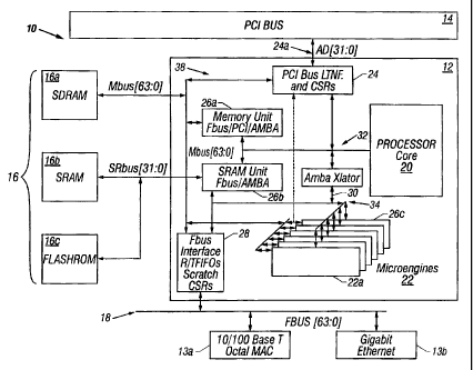
Referring to FIG. 1, a communication system 10
includes a parallel, hardware-based multithreaded processor
12. The hardware-based multithreaded processor 12 is
coupled to a bus such as a PCI bus 14, a memory system 16
and a second bus 18. The system 10 is especially useful
for tasks that can be broken into parallel subtasks or
functions. Specifically hardware-based multithreaded
processor 12 is useful for tasks that are bandwidth
oriented rather than latency oriented. The hardware-based
multithreaded processor 12 has multiple microengines 22
each with multiple hardware controlled threads that can be
simultaneously active and independently work on a task.
The hardware-based multithreaded processor 12 also
includes a central controller 20 that assists in loading
microcode control for other resources of the hardware-based
multithreaded processor 12 and performs other general
purpose computer type functions such as handling protocols,
exceptions, extra support for packet processing where the
microengines pass the packets off for more detailed
processing such as in boundary conditions. In one
embodiment, the processor 20 is a Strong Arm (Arm is a
trademark of ARM Limited, United Kingdom) based
architecture. The general purpose microprocessor 20 has an
operating system. Through the operating system the
processor 20 can call functions to operate on microengines
22a-22f. The processor 20 can use any supported operating
system preferably a real time operating system. For the
core processor implemented as a Strong Arm architecture,
-S-
CA 02391833 2002-02-26
WO 01/16782 PCT/US00/22322
operating :systems such as, MicrosoftNT real-time, VXWorks
and uCUS, a freeware operating system available over the
Internet, can be used.
The hardware-based multithreaded processor 12 also
includes a plurality of function microengines 2a?a-22f.
Functional microengines (microengines) 22a-22f each
maintain a plurality of program counrers in hardware and
states associated with the program counters. Effectively,
a corresponding plurality of sets of threads can be
simultaneously active on each of the microengines 22a-22f
while only one is actually operating at any one time.
In one embodiment, there are six microengines 22a-22f
as shown. Each microengines 22a-22f has capabilities for
processing four hardware threads. The six microengines
22a-22f operate with shared resources including memory
system 16 and bus interfaces 24 and 28. The memory system
16 includes a Synchronous Dynamic Random Access Memory
(SDRAM) controller 26a and a Static Random Access Memory
(SRAM) controller 26b. SDRAM memory 16a and SDRAM
controller 26a are typically used for processing large
volumes of data, e.g., processing of network payloads from
network packets. The SRAM controller 26b and SRAM memory
16b are used in a networking implementation for low
latency, fast access tasks, e.g., accessing look-up tables,
memory for the core processor 20, and so forth.
The six microengines 22a-22f access either the SDRAM
16a or SRAM 16b based on characteristics of the data.
Thus, low latency, low bandwidth data is stored i.n and
fetched from SRAM, whereas higher bandwidth data for which
latency is not as important, is stored in and fetched from
-6-
CA 02391833 2002-02-26
WU 01/16782 PCTNSU0/22322
SDRAM. The microengines 22a-22f can execute memory
reference instructions to either the SDRAM controller 26a
or SRAM controller 16b.
Advantages of hardware multithreading can be explained
by SRAM or SDRAM memory accesses. As an example, an SRAM
access requested by a Thread_0, from a microengine will
cause the SRAM controller 26b to initiate an access to the
SRAM memory 16b. The SRAM controller controls arbitration
for the SRAM bus, accesses the SRAM 16b, fetches the data
from the SRAM 16b, and returns data to a requesting
microengine 22a-22b. Uuring an SRAM access, if the
microengine e.g., 22a had only a single thread that could
operate, that microengine would be dormant until data was
returned from the SRAM. By employing hardware context
i5 swapping within each of the microengines 22a-22f, the
hardware context swapping enables other contexts with
unique program counters to execute in that same
microengine. Thus, another thread e.g., Thread 1 can
function while the first thread, e.g., Thread 0, is
awaiting the read data to return. During execution,
Thread i may access the SDRAM memory 16a. While Thread 1
operates on the SDRAM unit, and Thread-0 is operating on
the SRAM unit, a new thread, e.g., Thread_2 can now operate
in the microengine 22a. Thread 2 can operate for a certain
amount of time until it needs to access memory or perform
some other long latency operation, such as making an access
to a bus interface. Therefore, simultaneously, the
processor 12 can have a bus operation, SRAM operation and
SDRAM operation all being completed or operated upon by one
microengine 22a and have one more thread available to
CA 02391833 2002-02-26
WO 01/16782 PC'TIUS00/22322
process more work in the data path.
The hardware context swapping also synchronizes
completion of tasks. For example, two threads could hit
the same shared resource e.g., SRAM. Each one of these
separate functional units, e.g., the FBOS interface 28, the
SRAM controller 26a, and the SDRI1M controller 26b, when
they complete a requested task from one of the r~icroengi.ne
thread contexts reports back a flag signaling completion
of an operation. When the flag is received by the
microengine, the microengine can determine which thread to
turn on.
One example of an application for the hardware-based
multithreaded processor 12 is as a network processor. As a
network processor, the hardware-based multithreaded
processor 12 interfaces to network devices such as a media
access controller device e.g., a 10/100L3aseT Octal MAC 13a
or a Gigabit Ethernet device 13b. In general, as a network
processor, the hardware-based multithreaded processor 12
can interface to any type of communication device or
interface that receives/sends large amounts of data.
Communication system 10 functioning in a networking
application could receive a plurality of network packets
from the devices 13a, 13b and process those packets in a
parallel manner. With the hardware-based multithreaded
processor 12, each network packet can be independently
processed.
Another example for use of processor 12 is a print
engine for a postscript processor or as a processor for a
storage subsystem, i.e., RAID disk storage. A further use
is as a matching engine. In the securities industry for
_g_
CA 02391833 2002-02-26
WO 01116782 PCT/USOOIZ2322
example, the advent of electronic trading requires the use
of electronic matching engines to match orders between
buyers and sellers. These and other parallel types of
tasks can be accomplished on the system 10.
The processor 12 includes a bus interface 28 that
couples the processor to the second bus 18. Bus interface
28 in one embodiment couples the processor 12 to the so-
called FBUS 18 (FIFO bus;. The FBUS interface 28 is
responsible f_or controlling and interfacing the processor
12 to the FBUS 18. The FBUS 18 is a 64-bit wide FIFO bus,
used to interface to Media Access Controller (MAC) devices.
The processor 12 includes a second interface e.g., a
PCI bus interface 24 that couples other system components
that reside on the PCI 14 bus to the processor 12. The PCI
bus interface 24, provides a high speed data path 24a to
memory 16 e.g., the SDRAM memory 16a. Through that path
data can be moved quickly from the SDRAri 16a through the
PCI bus 14, via direct memory access (DMA) transfers. The
hardware based multithreaded processor 12 supports image
transfers. The hardware based multithreaded processor Z2
can employ a plurality of DMA channels so if one target of
a DMA transfer is busy, another one of the DMA channels can
take over the PCI bus to deliver information to another
target to maintain high processor 12 efficiency.
Additionally, the PCI bus interface 24 supports target
and master operations. Target operations are operations
where slave devices or: bus 14 access SDRAMs through reads
and writes that are serviced as a slave to target
operation. In master operations, the processor core 20
sends data directly to or receives data directly from the
_g_
CA 02391833 2002-02-26
WO 01116782 PCT/US0022322
PCI interface 24.
Each of the functional units are coupled to one or
more internal buses. As described below, the internal
buses are dual., 32 bit buses (i.e., one bus for read and
one for write). The hardware-based multithreaded processor
12 also is constructed such that the sum of the bandwidths
of the internal buses in the processor 12 exceed the
bandwidth of external buses coupled to the processor 12.
The processor 12 includes an internal core processor bus
32, e.g., an ASB bus (Advanced System Bus) that couples the
processor core 20 to the memory controller 26a, 26c and to
an ASB translator 30 described below. The ASB bus is a
subset of the so called AMBA bus that is used with the
Strong Arm processor core. The processor Z2 also includes
a private bus 34 that couples the microengine units to SRAM
controller 26b, ASB translator 30 and FF3US interface 28. A
memory bus 38 couples the memory controller 26a, 26b to the
bus interfaces 24 and 28 and memory system 16 including
flashrom 16c used for boot operations and so forth.
Referring to FIG. 2, each of the microengines 22a-22f
includes an arbiter that examines flags to determine the
available threads to be operated upon. Any thread from any
of the microengines 22a-22f can access the SDRAM controller
26a, SDRAM controller 26b or FBUS interface 28. The memory
controllers 26a and 26b each include a plurality of queues
to store outstanding memory reference requests. The queues
either maintain order of memory references or arrange
memory references to optimize memory bandwidth. For
example, if a thread'0 has no dependencies or relationship
to a thread 1, there is no reason t=hat thread 1 and 0
-10-
CA 02391833 2002-02-26
WO 01/16782 PCTNS00/22322
cannot complete their memory references to the SRAM unit
out of order. The microengines 22a-22f issue memory
reference requests to the memory controllers 26a and 26b.
The microengines 22a-22f flood the memory subsystems 26a
and 26b with enough memory reference operations such that
the memory subsystems 26a and 26b become the bottleneck for
processor 12 operation.
If the memory subsystem 16 is f.Looded with memory
requests that are independent in nature, the processor 12
can perform memory reference sorting. Memory reference
sorting improves achievable memory bandwidth. Memory
reference sorting, as described below, reduces dead time or
a bubble that occurs with accesses to SRAM. With memory
references to SRAM, switching current direction on signal
lines between reads and writes produces a bubble or a dead
time waiting for current to settle on conductors coupling
the SRAM 16b to the SRAM controller 26b.
That is, the drivers that drive current on the bus
need to settle out prior to changing states. Thus,
repetitive cycles of a read followed by a write can degrade
peak bandwidth. Memory reference sorting allows the
processor 12 to organize references to memory such that
long strings of reads can be followed by long strings of
writes. This can be used to minimize dead time in the
pipeline to effectively achieve closer to maximum available
bandwidth. Reference sorting helps maintain parallel
hardware context threads. On the SDRAM, reference sorting
allows hiding of pre-charges from one bank to another bank.
Specifically, if the memory system 16b is organized into an
3G odd bank and an even bank, while the processor is operating
-11-
CA 02391833 2002-02-26
WO 01/16782 PCT/US00/22322
on the odd bank, the memory controller r_an start
precharging the even bank. Precharg.ing is possible if
memory references alternate between odd and even banks. By
ordering memory references to alternate accesses to
opposite banks, the processor 12 improves SDRAM bandwidth.
Additionally, other optimizations can be used. For
example, merging optimizations where operations that can be
merged, are merged prior to memory access, open page
optimizations where by examining addresses ar: opened page
of memory is not reopened, chaining, as will be described
below, and refreshing mechanisms, can be employed.
The FBUS interface 28 supports Transmit and Receive
flags for each port that a MAC device supports, along with
an Interrupt flag indicating when service is warranted.
The FBUS interface 28 also includes a controller 28a that
performs header processing of incoming packets from the
FBUS 18. The controller 28a extracts the packet headers
and performs a microprogrammable
source/destination/protocol hashed lookup (used for address
smoothing) in SRAM. If the hash does not successfully
resolve, the packet header is sent to the processor core 20
for additional processing. The FBUS interface 28 supports
the following internal data transactions:
-12-
CA 02391833 2002-02-26
WO 01/16782 PCT'/US00/21,322
FBUS unit Shared bus SRAM) to/from microengine.
FBUS unit (via private bus) writes from SDRAM Unit.
FBUS unit (via Mbus) Reads to SDRAM.
The FBUS 18 is a standard industry bus and includes a
data bus, e.g., 64 bits wide and sideband control for
address and read/write control. The FBUS interface 28
provides the ability to input large amounts of data using a
series of input and output FIFO's 29a-29b. From the FIFOs
29a-29b, the microengines 22a-22f fetch data from or
command the SDRAM controller 26a to move data from a
receive FIFO in which data has come from a device on bus
18, into the FBUS interface 28. The data can be sent
through memory controller 26a to SDRAM memory 16a, via a
direct memory access. Similarly, the microengines can move
data from the SDRAM 26a to interface 28, out to FBUS 18,
via the FBUS interface 28.
-13-
CA 02391833 2002-02-26
WO 01/16782 PCT/USOO/ZZ322
Data functions are distributed amongst the
microengines. Connectivity to the SRAM 26a, SDRAM 26b and
BUS 28 is via command requests. A command request can be
a memory request or a FBUS request. For example, a
command request can move data from a register lccated in a
microengine 22a to a shared resource, e.g., an SDRAM
location, SRAM location, flash memory or some MAC address.
The commands are sent out to each of the functional units
and the shared resources. However, the shared resources do
not need tc maintain local buffering of the data. Rather,
the shared resources access distributed data located inside
of the microengines. This enables microenqines 22a-22f, to
have local access to data rather than arbitrating for
access on a bus and risk contention for the bus. With this
feature, there is a 0 cycle stall for waiting for data
internal to the microengines 22a-22f.
The data buses, e.g., ASB bus 30, SRAM bus 34 and
SDRAM bus 38 coupling these shared resources, e.g., memory
controllers 26a and 26b are of sufficient bandwidth such
that there are no internal bottlenecks. Thus, in order to
avoid bottlenecks, the processor 12 has an bandwidth
requirement where each of the functional units is provided
with at least twice the maximum bandwidth of the internal
buses. As an example, the SDRAM can run a 64 bit wide bus
at 83 MHz. The SRAM data bus could have separate read and
write buses, e.g., could be a read bus of 32 bits wide
running at 166 MHz and a write bus of 32 bits wide at 166
MHz. That is, in essence, 64 bits running at 166 MHz which
is effectively twice the bandwidth of the SDRAM.
-14-
CA 02391833 2002-02-26
WO 01/16782 PCT/US00/ZZ322
The core processor 20 also can access the shared
resources. The core processor 20 has a direct
communication to the SDRAM controller 26a to the bus
interface 24 and to SRAM controller 26b via bus 32.
However, to access the microengines 22a-22f and transfer
registers located at any of the microengines 22a-22f, the
core processor 20 access the microengi.nes 22a-22f via the
ASB Translator 30 over bus 34. The ASB translat=or 30 can
physically reside in the FBUS interface 28, but. logically
is distinct. The ASB Translator 30 performs an address
translation between FBUS microengine transfer register
locations and core processor addresses (i.e., ASB bus) so
that the core processor 20 can access registers belonging
to the microengines 22a-22c.
Although microengines 22 can use the register set to
exchange data as described below, a scratchpad memory 27 is
also provided to permit microengines to write data out to
the memory for other microengines to read. The scratchpad
27 is coupled to bus 34.
-15-
CA 02391833 2002-02-26
WO 01/16782 PCT/USOOIZ2322
'fhe processor core 20 includes a RISC: core 50
implemented in a five stage pipeline performing a single
cycle shift of one operand or two operands in a single
cycle, provides multiplication support and 32 bit barrel
shift support. This R~CSC core 50 is a standard Strong Army
architecture but it is implemented with a five stage
pipeline for performance reasons. The processor core 20
also includes a 16 kilobyte instruction cache 52, an 8
kilobyte data cache 54 and a prefetch stream buffer 56.
The core processor 20 ~~erforms arithmetic operations in
parallel with memory writes and instruction fetches. The
core processor 20 interfaces with other functional units
via the ARM defined AS13 bus. The ASB bus is a 32-bit bi-
directional bus 32.
Microengines:
Referring to FIG. 3, an exemplary one of the
microengines 22a-22f, e.g., microengine 22f. is shown. The
microengine includes a control store 70 which, in one
implementation, includes a RAM of here 1,024 words of 32
bit. The RAM stores a microprogram. The microprogram is
loadable by the core processor 20. The microengine 22f
also includes controller logic 72. The controller logic
includes an instruction decoder ;3 and program counter (PC)
units 72a-72d. The four micro program counters 72a-72d are
maintained in hardware. The microengine 22f also includes
context event switching logic 74. Context event logic 74
receives messages (e. g., SEQ_# EVENT RESPONSE:
FBI EVENT RESPONSE; SRAM EVENT RESPONSE; SDRAM
3C EVENT RESPONSES and ASR EVENT RESPONSE) from each one of
-16-
CA 02391833 2002-02-26
WO OI/16782 PCTNSOO/Z2322
the shared resources, e.g., SRAM 26a, SDRAM 26b, or
processor core 20, control and status registers, and so
forth. These messages provide information cn whether a
requested function has completed. Based on whether or not
a function requested by a thread has completed and signaled
completion, the thread needs to wait_ for that completion
signal, and if the thread is enabled to operate, then the
thread is placed on an available thread list (not shown).
The microengine 22f can have a maximum of e.g., 4 threads
available.
In addition to event signals that are local to an
executing thread, the microenqines 22 employ signaling
states that are global. With signaling states, an
executing thread can broadcast a signal state to all
microengines 22. Receive Request Available signal, Any and
all threads in the microengines can branch on these
signaling states. These signaling states can be used to
determine availability of a resource or whether a resource
is due for servicing.
The context event logic 74 has arbitration for the
four (4) threads. In one embodiment, the arbitration is a
round robin mechanism. Other techniques could be used
including priorii.y queuing or weighted fair queuing. The
microengine 22f also includes an execution box (EBOX) data
path 76 that includes an arithmetic logic unit 76a and
general purpose register set 76b. The arithmetic logic
unit 76a performs arithmetic and logical functions as well
as shift functions. The registers set 76b has a relatively
large number of general purpose registers. As will be
described in FIG. 3B, in this implementation there are 69
-17-
CA 02391833 2002-02-26
WO 01116782 PCT/US00I22322
general purpose registers in a first bank, Bank A and 64 in
a second bank, Bank B. The general purpose registers are
windowed as will be described so that they are relatively
and absolutely addressable.
The microengine 22f also includes a write transfer
register stack 78 and a read transfer stack 80. These
registers are also windowed so that they are re~~.atively and
absolutely addressable. Write transfer register stack 78
is where write data to a resource is located. Similarly,
read register stack 80 is for return data from a shared
resource. Subsequent to or concurrent with data arrival,
an event signal from the respective shared resource e.g.,
the SRAM controller 26a, SDRAM controller 26b or core
processor 20 will be provided to context event arbiter 74
which will then alert the thread that the data i.s available
or has been sent. Both transfer register banks 78 and 80
are connected to the execution box (EBOX) 76 through a data
path. In one implementation, the read transfer register
has 64 registers and the write transfer register has 64
registers.
As shown in FIG. 3A, the microengine datapath
maintains a 5-stage micro-pipeline 82. This pipeline
includes lookup of macroinstruction words 82a, formation of
the register file addresses 82b, read of operands from
register file 82c, ALU, shift or compare operations 82d,
and write-back of results to registers 82e. By providing a
write-back data bypass into the ALU/shifter units, and by
assuming the registers are implemented as a register file
(rather than a RAM), the microengine can perform a
simultaneous register file read and write, which completely
-18-
CA 02391833 2002-02-26
WO 01/16782 PCT/US00/22322
hides the write operation.
The SDR.AM interface 26a provides a signal back to the
requesting microengine on reads that indicates whether a
parity error occurred on the read request. The microengine
microcode is responsible for checking the SDRAM read Parity
flag when the microengine uses any return data. Upon
checking the flag, if it was set, the act of branching on
it clears it. The Parity flag is only sent when the SDRAM
is enabled for checking, and the SDRAM is parity protected.
The microengines and the PCI Unit are the only requestors
notified of parity errors. Therefore, if the processor
core 20 or FIFO requires parity protection, a microengine
assists in the request. The microengines 22a-22f support
conditional branches. The worst case conditional branch
latency (not including jumps) occurs when the branch
decision is a result of condition codes being set by the
previous microcontrol instruction. The latency is shown
below in Table 1:
-19-
CA 02391833 2002-02-26
WO 01/16782 PCT/USOOlZ232Z
I 1 I 2 I 4 I I I '
3 I 5 fp ~ 8
I
_________________~____+____+____+ ____~____+____+____t_____~
microstore lookvlp . n'. I n2 XX I b2 b3
cb I I b1 I I
'
b9 J
reg addr gen I I n1 I XX I I f I
cb J XX b1 b2 b3
I
reg file lookup I I I n1 cb I I I I
J XX XX b1 b2
I
ALU/shifter/cc I I l I n1 I J J I
cb XX XX b1
I
write back I I I m21 f I J I
n~ cb XX XX
I
where nx is pre-branch microword (n1 sets cc's)
cb is conditional branch
bx is post-branch microword
XX is aborted microword
As shown in Table 1, it is not until cycle 4 that the
condition codes of n1 are set, and the branch decision can
be made (which in this case causes the branch path to be
looked up in cycle 5). The microengine incurs a 2-cycle
branch latency penalty because it must abort operations n2
and n3 (the 2 microwords directly after the branch) in the
pipe, before the branch path begins to fill the pipe with
operation b1. If the branch is not taken, no microwords
are aborted and execution continues normally. 'rhe
microengines have several mechanisms to reduce or eliminate
the effective branch latency.
_20_
CA 02391833 2002-02-26
WO 01/16782 PCTIUS00/22322
The microengines support deferred branches. Deferring
branches are when a microengine allows 1 or 2 microwords
after the branch to occur before the branch takes effect
(i.e. the effect of the branch is "deferred" in time).
Thus, if useful work can be found to fill the wasted cycJ.es
after the branch microword, then the branch latency can be
hidden. A 1-cycle deferred branch is shown below where n2
is allowed to execute after cb, but before b1:
I 1 I 2 I 3 I 4 I 5 l 6 I ~ I B I
_________________+____+____+____+____+____+_____+____+____+
microstore lookup I n7 ! cb I n2 I XX I b~. I b2 I b3 I
b4 I
reg addr gen I I n1 1 cb I n2 I XX I b1 I b2 I b3 I
reg file lookup l I I n1 I cb I n2 I XX I b1 I b2 I
ALU/shifter/cc I I I ! n1 I cb I n2 I XX I b1 I
write back I I I I I n1 I <:b I n2 I XX I
A 2-cycle deferred branch is shown below, where n2 and
n3 are both allowed to complete before the branch to b1
occurs. Note that a 2-cycle branch deferment is only
allowed when the condition codes are set on the microword
preceding the branch.
I 1 I 2 I 3 I 4 I 5 I 6 I ~ I 8 I 9 I
______________+____+____+____+____+____+____+____r.____
microstore lookup I n1 I cb I n2 I n3 ; b1 I b2 I b3 I b4 I b5 I
reg addr gen I I n1 I cb I n2 I n3 I b1 ! b2 I b3 I b4 I
reg file lkup I I I n1 I cb I n2 I n3 I b1 I b2 I b3 I
ALU/shftr/cc ! I I I n1 I cb I n2 I n3 I b1 I b2 I
write back I I I I I n1 I cb ! n2 I n3 I b1 I
-21-
CA 02391833 2002-02-26
WO 01/16?82 PCTNS00/1Z32Z
The microengi.nes also support condition code
evaluation. 1f the condition codes upon which a branch
decision are made are set 2. or more microwords before the
branch, then 1 cycle of branch latency can be eliminated
because the branch decision can be made 1 cycle earlier:
1 I 2 I 3 I I I I I 8 I
4 5 6 7
_________________+____+____+____;.____ +____+____+____+____+
microstore lookup I n1 I n2 I XX b1 b2 b3 I
cb I I I I b4 I
reg addr gen ! I n1 I n2 I I I I I b3
cb XX b1 b2 I
reg file lookup I I I n-L I n2 I I I I b2
cb XX b1 I
AhU/shifter/cc ( I I I n1 I I I I b1
n2 cb XX I
write back I I I l I I I I XX
n1 n2 cb
1n this example, n1 sets the condition codes and n2
does not set the conditions codes. 'therefore, the branch
decision can be made at cycle 4 (rather than 5), to
eliminate 1 cycle of branch latency. In the example below,
the 1-cycle branch deferment and early setting of condition
codes are combined to completely hide the branch latency:
Condition codes (cc's) set 2 cycles before a 1-cycle
deferred branch:
I 1 I 2 I 3 I 4 I I I I 8 I
5 6 ~
_________________
microstore lookup I n1 I n2 I cb b1 b2 b3 I
I n3 I I b4 I
reg addr gen I f n7 I n2 I cb f I ( b3
I n3 b/ b2 I
reg file lookup I . I n1 I n2 I cb I I I b2
n3 b1 I
ALU/shi.fter/cc I I I I n1 I n2 I I I b1
cb n3 I
write back I I I I I n1 I I I n3
n2 cb I
-22-
CA 02391833 2002-02-26
WO 01!16782 PCf/US00/22322
In the case where the condition codes cannot be set
early (i.e. they are set i.n the microword preceding the
branch), the microengine supports branch guessing which
attempts to reduce the 1 cycle of exposed branch latency
that remains. By "guessing" the branch path or the
sequential path, the microsequencer pre-fetches the guessed
path 1 cycle before it definitely knows what path to
execute. If it guessed correctly, 1 cycle of branch
latency is eliminated as shown below:
guess branch taken /branch is taken
I 1 I 2 1 '~ I 9 I 5 I 6 I ~ I 8 I
_________________+____+____+___._+_.___+____+____+____+____+
microstore lookup I n! I cb b! b2 b3 b4 I
I n:1 I I I I b5
I
reg addr gen I I n! I cb I I I I b4
I XX b! b2 b3 I
reg file lookup I I I n! I cb I I I I b3
XX b! b2 I
Ai:U/shi.fter/cc f I I I n! I I I I b2
cb XX b! I
write back I I I I I I I I b!
n! cb XX I
If the microcode guessed a branch taken incorrectly, the
microengine still only wastes 1 cycle:
-23-
CA 02391833 2002-02-26
WO 01116782 PCT/US00/22322
guess branch taken /branch is NOT taken
I 1 I 2 I 3 5 6 7 8 I
I 4 I I I I
_________________+____+____+____+____ +____+____+____f____+
microstore lookup I n1 I cb XX n2 n3 n9 i
I n1 I I I I n5
I
reg addr gen I I n1 I cb I I I I n4
I n1 XX m2 n3 I
reg file lookup I I f n1 i I I I I n3
cb n1 XX n2 I
ALU/shifter/cc I I 1 I n1 I I I I n2
cb n1 XX 1
write back I I i I I I I I XX
=~1 ch n1
However, the latency penalty is distributed
differently when microcode guesses a branch is not taken:
For guess branch NOT taken / branch is NOT taken there
are no wasted cycles as set out below.
I 1 I 2 I 3 I I ! I I 8
9 5 6 ~ I
_________________+____+____t____+____ +____+____+____+____+
microstore lookup I n1 I cb I n2 n3 n4 n5 1
n1 I I I r.6
I
reg adds gen I I n1 I cb I I I I I n5
n1 n2 n3 n4 I
recd file lookup I I I r11 I cb I I I I b4
n1 n2 n1 I
ALU/shifter/cc I I I I n1 i I I I n3
cb n1 n?_ I
write back I I I 1 I ! I I n2
n~. cb n~
However for guess branch NC?T taken /branch is taken
there are 2 wasted cycles.
I 1 I 2 I 9 5 6 7 I
3 I I I I 8
I
_________________+____+____+____+____ +____+____+____+____+
microstore lookup I n1 I cb XX b1 b2 b3
I n1 I I I I I
b4 I
reg addr gen I I n2 1 cb I I I I b3
I XX XX b7. b?.I
reg file lookup I I i n1 I cb I I i i b2
XX XX b1 I
ALU/shifter/cc I I I I n1 I I I I b1
cb XX XX I
write back I I I I I I I I XX
n1 cb XX I
_29 _
CA 02391833 2002-02-26
WO 01/16782 PC1'/USOOIIZ322
The microengine can combine branch guessing with 1-cycle
branch deferment to improve the result further. For guess
branch taken with 1-cycle deterred branch/branch is taken
is:
i 1 I 2 t 3 I 4 I 5 I 6 I 7 i 8 I
_________________+____+____+____+____+____+____+____+____+
microstore lookup I n1 I cb b1 b2 b3 b4 I
I n1 I I I ( b5
I
reg addr gen I I nI I cb I I I i b4
I n2 b1 b2 b3 I
reg file lookup I I I n1 I cb I I ( I b3
n2 b1 b2 I
ALU/shifter/cc I I I I n1 I I ( I b2
cb n2 b1 I
write back I J I I I I I I b1
rllcb n2 I
In the case above, the 2 cycles of branch latency are
hidden by the execution of n2, and by correctly guessing
the branch direction. If microcode guesses incorrectly, 1
cycle of branch latency remains exposed as shown below:
guess branch taken with 1-cy::le deferred branch/branch is
NOT taken
I 1 I I I 3 I 4 I 5 I 6 I 7 I F3 I g I
______________+____+____~.____+____,____.+____+____,____,____,.
microstore lookup I n1 I cb I n2 I XX ( n3 I n9 I n5 I n6 I n7 (
reg addr gen f I n1 I cb I n2 ! XX I n3 I n9 ; n5 ( r6 I
reg file lkup I I 1 n1 f cb I n2 I XX I n3 I n9 I n5 (
ALU/shftr/cc I I I I n1 I ;:b I n2 ( XX I n3 ( n4 I
write back I 1 I I I n1 '~, cb I n2 I XX ( n3 I
-25-
CA 02391833 2002-02-26
wo om6~s2 rc~rn~soonZ3Zz
If microcode correctly guesses a branch NOT taken,
then the pipeline flows sequentially in the normal
unperturbed case. If :microcode incorrectly guesses branch
NOT taken, the microengine again exposes 1 cycle of
unproductive execution as shown below:
guess branch NOT taken/branch i.s taken
I 7 I 2 I 3 I 4 I 5 I 6 I ~ I 8 I 9 I
1p ______________+____+____+____+__.__+____+____+____+____+____+
microstore lookup ; n1 I cb I n~' f XX I b1 I b2 I b3 ( b9 I b5 I
reg addr gen I I n1 ! cb I n2 I XX ! b1 r b2 I b3 ! b4 !
reg file lkup I I I n1 I c:b I n2 I XX I b1 I b2 I b3 I
F1LU/s:Wtr/cc I I I I n? ! cb I n2 I XX I b1 I b2 I
write back I I I I f n1 I rb I n2 I XX f b1 I
where nx is pre-branch microword (n1 sets cc's)
cb is conditional branch
bx is port-branch microword
XX is aborted microword
In the case of a jump instruction, 3 extra cycles of
latency are incurred because the branch address is not
known until the end oi- the cycle in which the jump is in
the ALD stage:
1 I 2 I 3 I 9 I 5 I 6 I 7 I 8 I
______________+___._+____+____+____+____+____+____+____+____+
micrcstore lookup I n1 I jp I XX I XX I XX I j1 I j2 I j3 I j4
req addr qen I 1 n1 I jp i XX I XX ; XX I j1 I j~ I j3 I
reg file lkup I I I n1 I jp I XX I XX I XX I j1 I j2 I
ALU/shftr/cc I I I I n1 I jp XX I XX I XX I j1 1
wri to back I I I I I n1 ; jp I XX I XX I XX !
-26-
CA 02391833 2002-02-26
WO 01 /16782 PCTNS00/Z2322
Context Switch:
Referring to FIG. 3B, a format from a context switch
instruction is shown. A context switch is a special form
of a branch that causes a different context (and associated
PC) to be selected. Context switching introduces some
branch latency as well. Consider the following context
switch:
I 1 I 2 I 3 I 4 I 5 I 6 I ~ I ~ I 9 I
______________+____~____.+____~-____+____+____+____+____+____+
micros~ore lookup I of I ca ( br I n1 I n2 I n3 I n4 i n5 I n6 I
reg adcr gen I of I ca I XX I n1 I n2 I n3 I n4 I n5 I
reg file lkup 1 I of I ca ! XX I n1 I n2 I n3 I n4 I
ALU/shftr/cc w I I ~1 I ca I xx I n1 I n2 I n3 I
write back ' I '~ I of I ca I XX I n1 I n2 I
where ox is old context flow
br is branch microword in old context
2 0 ~a is context rearbitration (causes context
switch)
nx is new context flow
XX is aborted microword
In a context switr_h the "br" microword is aborted to
avoid control and timing romplex~ties that could be caused
by saving the correct old contexl: PC.
Conditional branches that operate on ALU condition
codes which are set on the microword before the branch can
select 0, 1 or 2-cycle branch de-Ferment modes. Condition
codes set 2 or more microwords before the conditional
branch that operates cn them can select 0 or i-cycle branch
deferment modes. A1.1. other bran'~hes (including context
rearbitrations) can select either 0 or 1-cycle branch
-27-
CA 02391833 2002-02-26
WO 01/16782 PCT/USDO/Z2322
deferment modes. The architecture could be designed to
make a context arbitration microword within a branch
deferment window of a preceding branch, jump or context
arbitration microword, an illegal option. That is, in some
embodiments, a context switch would not be allowed to occu.c
during a branch transition in the pipeline because as
mentioned, it could unduly complicate saving of the old
context PC. The architecture could also be designed to
make branching within the branch deferment window of a
'w0 preceding branch, jump or context arbitration microword
illegal to avoid complicated and possible unpredictable
branch behaviors_
Each microengine 22a-22f supports multi-threaded
execution of four contexts. One .reason for this is to
allow one thread to start executing just after another
thread issues a memory reference and must wait until that
reference completes befcre doing more work. This behavior
is critical to maintaining efficient hardware execution of
the microengines because memory latency is significant.
Stated differently, if only a single thread exe<:ution was
supported, the microengines would sit idle for a
significant number of cycles waiting for references to
return and thereby reduce overall computational throughput.
Multi-threaded execution allows an m.icroengines to hide
memory latency by performing useful .independent work across
several threads. Two synchronization mechanisms are
supplied in order to allow a thread to issue an SRAM or
SDRAM reference, and then subsequently synchronize to the
point in time when that reference completes.
-28-
CA 02391833 2002-02-26
WO 01/16782 PCTIUS00122322
One mechanism is Immediate Synchronization. In
immediate synchronization, the microengine issues the
reference and immediately swap out that context. The
context will be signaled when the corresponding reference
completes. Once signaled, the context will be swapped back
in for execution when a context-swap event occurs and it is
its turn to run. Thus, from the point of view of a single
context's instruction stream, the microword after issuing
the mem reference does not get executed until the reference
completes.
A second mechanism is Delayed Synchronization. In
delayed synchronization, the microengine issues the
reference, and then continues to execute some other useful
work independent of the reference. Some time later it
could become necessary to synchronize the thread's
execution stream to the completion of the issued reference
before further work is performed. At this point a
synchronizing microword is executed that will either swap
out the current thread, and swap it back in sometime later
when the reference has completed, or continue executing the
current thread because the reference has already completed.
Delayed synchronization is implemented using two different
signaling schemes:
If the memory reference is associated with a transfer
register, the signal from which the thread is triggered is
generated when the corresponding transfer register valid
bit is set or cleared. For example, an SRAM read which
deposits data into transfer register A would be signaled
when the valid bi.t for A is set. If the memory reference
is associated with the transfer FIFO or the receive FIFO,
-2 9-
CA 02391833 2002-02-26
WO 01/16782 PCTlUS00/22322
instead of a transfer register, then the signal is
generated when the reference completes in the SDRAM
controller 26a. Only one signal .state per context is held
in the microengines scheduler, thus only one outstanding
signal can exist in this scheme.
There are at least two general. operat;~onal paradigms
from which microcontroller micro-programs could be
designed. One would be that overall microcontroller
compute throughput and overall memory bandwidth are
optimized at the expense of single thread execution
latency. This paradigm would make sense when the system
has multiple microengines executing multiple threads per
microengine on unrelated data packets.
A second one is that microengine execution latency
should be optimized at the expense of overall microengine
compute throughput and overall memory bandwidth. This
paradigm could involve execution of a thread with a real-
time constraint, that is, a constraint which dictates that
some work must absolutely be done by some specified time.
Such a constraint requires that optimization of the single
thread execution be given priority over other
considerations such as memory bandwidth or overall
computational throughput. A real-time thread would imply
a single microengine that executes only one thread.
Multiple threads would not be handled because the goal is
tc allow the single real-time thread to execute as soon as
possible--execution of multiple threads would hinder this
ability.
The coding style of these two paracigms could be
significantly different with regard r_o issuing memory
-30-
CA 02391833 2002-02-26
WO 01/16782 PCT/USOOIZ2322
references and context switching. In the real time case,
the goal is to issue as many memory references as soon as
possible in order to minimize the memory latency incurred
by those references. Having issued as many references as
early as possible the goal would be to perform as many
computations as the rnicroeng9.nes as possible in parallel
with the references. A computation flow that corresponds
to real-time optimization is:
0) issue mem ref 1
o) issue mem ref 2
o) issue mem ref 3
o) perform work independent of mem refs 1, 2 and 3
o) synch to completion of mem ref 1
0) perform work dependent on mem ref 1 and independent of mem ref 2
and 3
o) issue any new mem refs based on precedinc work.
o) synch to completion of mem ref 2
o) perform work dependent vn mem ref 1 and 2 independent of mem ref
3
o) issue any new rnem refs based on preceding work.
o) synch to completion of mem ref 3
o) perform work dependent on the completion of ail 3 refs
o) issue any nPw mem refs bused on preceding work.
In contrast, optimization for throughput and bandwidth
would take a different approach. With optimization for
microengine computational throughput and overall memory
bandwidth less consideration is given to single thread
execution Latency. To accomplish this, the goal would be
to equally space memory references across the microprogram
for each thread. This would provide a uniform stream of
memory references to the SRAM and SURHM controllers and
-31-
CA 02391833 2002-02-26
WO 01/16782 PC'TlUS00122322
would maximize the probability that 1 thread is always
available tc hide the memory latency incurred when another
thread is swapped out.
Register file address types:
Referring to FIG. 3C, the two register address spaces
that exist are Locally accessibly regisi.ers, and Globally
accessible registers accessible by all microengines. The
General Purpose Registers (GPRs) are implemented as two
separate banks (A bank and B bank) whose addresses are
interleaved on a word-by-word basis such that A bank
registers have lsb-0, and B bank registers have lsb-1.
Each bank is r_apable of performing a simultaneous read and
write to two different words within its bank.
Across banks A and B, the register set 76b is also
organized into four windows 76b~-76b3 of 32 registers that
are relatively addressable per thread. Thus, thread 0 wi7.l
find its register 0 at 77a (register 0), the thread 1 will
find its register 0 at 77b (register 32), thread 2 will
f;~nd its register 0 at 77c (register 69), and thread 3 at
77d (register 96). Relative addressing is supported so
that multiple threads can use the exact same control store
and locations but access different windows of register and
perform different functions. The uses of register window
addressing and bank addressing provide the requisite read
bandwidth using only dual ported RAMS in the microengine
22f.
These windowed registers do not have to save data from
context-switch to context switch so that the normal push
and pop of a context swap file or slack is eliminated.
-32-
CA 02391833 2002-02-26
WO Ot/16782 PCT/US00/2Z322
Context switching here has a 0 cycle overhead far changing
from one context to another. Relative register addressing
divides the register banks into windows across the address
width of the general purpose register set. Relative
addressing allows access any of the windows relative to the
starting point of the window. Absolute addressing .is also
supported in this architecture where any one of the
absolute registers may be accessed by any of thc: threads by
providing the exact address of the register.
Addressing of general purpose registers 78 can occur.
in 2 modes depending on the microword format. The two
modes are absolute and relative. In absolute mode,
addressing of a register address is directly specified i.n
7-bit source field (a6-a0 or b6-b0):
7 6 5 4 3 2 1 0
+---+---+---+---+---+---+ ---+---+
A GPR: I a61 0 a51a91a31a21all a01a6=0
~
B GPR: ( b61 1 b51b4~b31b21bll b0~b6-0
~
2 0 SRAM/ASB:I a61 a5~a410 a3~a2.1all a01a6=1, a5=0,
I a4=0
SDRAM: I a61 a51a410 a31a21all a01a6=l, a5=0,
~ a4=1
register address directly specified in 8-bit dent field
(d7-d0):
?5
7 6 5 4 3 2 1 0
+---+---+---+---+---+---+---+---+
A GPR: . d71 d61d51d4~d31d21dlld01d7=0,d6=0
B GPR: I d7~ d61d51d41d31d21dlld01d7=0,d6-1
3 0 SRAM/ASB:I d71 d6)d51d4~d31d2~d1id01d7=1,d6=0,
d5=0
SDRAM: d71 d61d51d41d31d21d1 d(11d7=7,d6=0,
d5=-
-33-
CA 02391833 2002-02-26
WO OII1678Z PCTIUSOO/Z232Z
if <a6:a5>=1,1, <b6:b5>-1,1, or <d7:d6>=1,1 then the
lower bits are pnterpreted as a context-relative address
field (described below). When a non-relative A or B source
address is specified in the A, B absolute field, only the
Iower half of the SRAM/ASB and SDRAM address spaces can be
addressed. Effectively, reading absolute SRAM/SDRAM
devices has the effective address space; however, since
this restriction does not apply to tre dest field, writing
the SRAM/SDRAM still uses the full address space.
In relative mode, addresses a specified address i.s
offset within context space as defined by a 5-bit source
field (a4-a0 or b4-b0):
7 6 5 4 3 2 1 0
+---+---+---+---+---+---+---+---+
A GPR: I a41 0 ~context~ a31 a21 a1 a0~ a4=0
B GPR: I b4~ 1 context) b31 b21 blJ b01 b4-=0
SRAM/ASB:lab4~ 0 Jab3lcontext~ bZl bl~ab0( ab9=1, ab3=0
SDRAM: (ab41 0 1ab31contextJ b21 b11ab01 ab4=1, ab3=1
or as defined by the 6-bit dent field (d5-d0):
7 6 5 9 3 2 1 0
+___t___+___+___+___+___+___+___+
A GPR: ( d51 d4lcontextl d21dlJd01 d5=0,d4=0
d3~
B GPR: I d5J d9lcontextl d2~dlld01 d5~0,d4=1
d31
SRAM/ASB:J d5J d41 d3~contextldy dl.~d01 d5=~l,d4=0,
d3=0
SDRAM: I d51 d41 d3lcontextJd?.IdlJd01 d5=1,d4=0,
d3=1
If <d5:d4>=1,1, then the destination address does
not address a valid register, thus, nc dest operand is
written back.
-34-
CA 02391833 2002-02-26
WO 01116782 PCT/US00/22322
The following registers are globally accessible from
the microengines and the memory controllers:
hash unit registers
scratchpad and common registers
receive FIFO and receive status FIFO
transmit FIFO
transmit control FIFO
The micrcengines are not interrupt driven. Each microflow
executes until completion and then a new flow is chosen
based an state signaled by other devices in the processor
12.
Referring to FIG. 4, the
SDRAM memory controller 26a includes memory reference
queues 90 where memory reference requests arrive from the
various microengines 22a-22f. The memory controller 26a
includes an arbiter 91 that selects the next the
microengine reference requests ~o go to any of the
functioning units. Given that one of the microengines is
providing a reference request, the reference request will
2C come through the address and command queue 90, inside the
SDRAM controller 26a. If the reference request has a bit
set called the "optimized MEM bit" the incoming reference
request will be sorted into either the even bank queue 90a
or the odd hank queue 90b. If the memory reference request
does not have a memory optimization bit set, the default
will be to go into an order queue 90c. The SDRAM
controller 26 is a resource which is shared among the FBUS
interface 28, the core processor 20 and the PCI interface
24. The SDRAM controller 26 also maintains a state machine
for performing READ-MODIFY-Write atomic operations. The
-35-
CA 02391833 2002-02-26
WO 01!16782 PCTIUS00/22322
SDRAM controller 26 also performs byte alignment for
requests of data from SDRAM.
The order queue 90c maintains the order of reference
requests from the microengines. With a series of odd and
even banks references it may be required that a signal is
returned only upon completion of a sequence of memory
references to both the odd and even banks. If the
microengine 22f sorts the memory references into odd bank
and even bank references and one of the banks, e.g., the
even bank is drained of memory references before the odd
bank but the signal is asserted on the last even reference,
the memory controller 26a could conceivably signal back to
a microengine that the memory request had completed, even
though the odd bank reference had not been serviced. This
1.5 occurrence could cause a coherency problem. The situation
is avoided by providing the order queue 90c allowing a
microengine to have multiple memory references outstanding
of which only its last memory reference needs to signal a
completion.
The SDRAM controller 26a also includes a high priority
queue 90d. In the high priority queue 90d, an incoming
memory reference from one of the microengines goes directly
to the high priority queue and is operated upon at a higher
priority than other memory references in the other queues.
All of these queues, the even bank queue 90a, the odd bank
queue 90b, the order queue 90c and the high priority queue,
are implemented in a single RAM structure that i.s logically
segmented snto four different windows, each window having
its own head and tail pointer. Since filling and draining
:30 operations are only a single input and a single output,
-36-
CA 02391833 2002-02-26
WO 01/16782 PCTIUSOOI22322
they can be placed into the same RAM structure to increase
density of RAM structures.
The SDRAM controller 26a also includes core bus
interface logic i.e., ASB bus 92. The ASB bus interface
logic 92 interfaces the core processor 20 tc the SDRAM
controller 26a. The ASB bus is a bus that includes a 32
bit data path and a 28 bit address path. The data is
accessed to and from memory through MEM ASB data device 98,
e.g., a buffer. MEM ASB data device 98 is a queue for
write data. If there is incoming data from the core
processor 20 via ASB interface 92, the data can be stored
i.r_to the MEM ASB device 98 and subsequently removed from
MEM ASR device 98 through the SDRAM interface 110 to SDRAM
memory 16a. Although not shown, the same queue structure
can be provided for the reads. The SDRAM controller 26a
also includes an engine 97 to pull data from the
microengines and PCI bus.
Additiona'~ queues include the P;:I address queue 94 and
ASB read/write queue 96 that maintain a number of requests.
The memory requests are sent to SDRAM interface 110 via
multiplexes 106. 'The multiplexes 106 is controlled by the
SDRAM arbiter 91 which detects the fullness of each of the
queues and the status of the requests and from that decides
priority based on a programmable value stored in a priority
service control register 100.
Once control to the multiplexes 106 selects a memory
reference request, the memory reference request, is sent to
a decoder I08 where it is decoded and an address is
generated. The decoded address is sent to the SDRAM
interface 110 where it is decomposed into row and column
CA 02391833 2002-02-26
WO 01/16782 PCTNS00/12322
address strobes to access the SDRAM 7.6a and write or read
data over data lines 16a sending data to bus 112. In one
implementation, bus 112 is actually two separate buses
instead of a single bus. The separate buses would include
S a read bus coupling the distributed mi.croengines 22a-22f
and a write bus coupling the distributed microengines 22a-
22f.
A feature of the SDRAM controller 26a is that when a
memory reference is stored in the queues 90, in addition to
the optimized MEM bit that can be set, there is a "chaining
bit". The chaining bit when set allows for special handling
of contiguous memory references. As previously mentioned,
the arbiter 12 controls which microengine will be selected
to provide memory reference requests over the commander bus
to queue 90 (FIG. 4l. Assertion of the chain bit will
control the arbiter tc have the arbiter select the
functional unit which previously requested that bus because
setting of the chain bit indicates that the microengine
issued a chain request.
Contiguous memory references will be received in queue
90 when the chaining bit is set. Those contiguous
references will typically be stored in the order queue 90c
because the contiguous memory references are multiple
memory references from a single thread. In order to
provide synchronization, the memory controller 26a need
only signal at the end of the chained memory references
when done. However, in an optimized memory chaining,
(e..g, when optimized MEM bit and chaining bit are set) the
memory references could go into different banks and
potentially complete on one of the banks issuing the signal
_38_
CA 02391833 2002-02-26
WO 01116782 PCT/USOO/ZZ322
"done" before the other bank was fully drained, thus
destroying coherency. Therefore, the chain bit is used by
the controller 170 to maintain the memory references from
the current queue.
Referring to FIG. 4A, a flow representation of the
arbitration policy in the SDRAM controller 26a is shown.
The arbitration policy favors chained microengine memory
requests. The process 115 starts by examining for Chained
microengine memory reference requests llSa . The process
115 stays at the chained requests until the chain b it is
cleared. The process examines ASB bus requests 115b
followed by PCI bus requests 115c, I-Sigh Priority Queue
Service 115d, Opposite Bank Requests 115e, Order Queue
Requests 115f, and Same Bank Requests 1158. Chained
request are serviced completely, whereas services 115b-115d
are serviced in round robin order. Only when services
115a-115d are fully drained does the process handle
services 115e-1158. Chained microengine memory reference
requests are when the previous SDRAM memory request has the
chain bit set. When the chain bit is set then the
arbitration engine simply services the same queue again,
until the chain bit is cleared. The ASB is higher priority
than PCI due to the severe performance penalty imposed on
the Strong arm core when the ASB is in wait state. PCI has
higher priority than the microengines due to the latency
requirements of PCI. However with other buses, the
arbitration priority could be different.
As shown in FIG. 4B, typical timing of a memory
without active memory optimization and with active memory
optimization is shown. As can be seen, the use of active
-39-
CA 02391833 2002-02-26
WO 01/16?82 PCT/1JS00/2Z322
memory optimizations m«ximizes the use of the bus and thus
hides the inherent latency within physical. SnRAM devices.
In this example, a non--optimized access can take 14 cycles
while optimiLed access can take 7 cyles.
Referring to FIG. 5, the memory controller 26b for the
SRAM is shown. The merlory controller 26b includes an
address and cor<unand queue 120. While the memory controller
26a (FIG. 4) has a queue for memory optimization based on
odd and even banking, memory controller 26b is optimized
based on the type of mE:mory operation, i.e., a read or a
write. The address and cornmand queue 120 includes a high
priority queue 120x, a read queue 120b which is the
predominant. memory reff~rence function that an SRAM
performs, and an order queue 120c which in general will
include all writes r_o 3RAM and reads that are to be non-
optimized. Although not shown, the address and command
queue i20 could also include a write queue.
The St-tAM controll~=r 26b also includes core bus
interface logic i.e., ,rISB bus 122. The ASB bus interface
logic 122 interfaces the r_ore processor 20 to the SRAM
controller 26b. The ASB bus is a bus that includes a 32
bit data path and a 2B bit addre~~s path. The data is
accessed to and from memory through MEM ASB data device
128, e.g., a buffer. MEM ASB data device 12$ is a queue
for write data. If there is incoming data from the core
processor 20 via ASB interface 122, the data can be stored
into the MEM ASB device 128 and subsequently removed from
MEM ASB device 128 through SRAM interface 140 to SRAM
memory 16b. Although not shown, the sane queue structure
can be provided for reads. The ;SRAM controller 26b also
-40-
CA 02391833 2002-02-26
WO 01/16782 PCT/US00/12322
includes an engine 127 to pull data from the microengines
and PC1 bus.
'the memory requests are sent to SRAM interface 140 via
multiplexes 126. The multiplexes 126 is controlled by the
SRAM arbiter 131 which detects the fullness of each of the
queues and the status of the requests and from that decides
priority based on a programmable value stored in a priority
service control register 1.30. Once control to the
multiplexes 126 selects a memory .reference request, the
memory reference request, is sent. to a decoder 138 :where jt
is decoded and an address is generated.
The SRAM Unit maintains control of the Memory Mapped
off-chip SRAM and Expansion ROM. fhe SRAM controller 26b
can address, e.g., 16 MBytes, with, e.g., 8 MBytes mapped
for SRAM 16b, and 8 MBytes reserved for special functions
including: Boot space via flashrom 16c; and Console port
access for MAC devices 13a, 13b and access to associated
(RMON) counters. The SRAM is used for local look-up tables
and queue management functions.
The SRAM controller 26b supports the following
transactions:
Microengine requests (via private bus; to/from SRAM.
Core Processor (via ASB bus) tolfrom SRAM.
The SRAM controller 26b performs memory reference
sorting to minimize delays (bubbles) in the pipeline from
the SRAM interface 14U to memory 16b. The SRAM controller
26b does memory reference scrting based on the read
function. A bubb-~e can either be 1 or 2 cycles depending
on the type of memory device employed.
-41-
CA 02391833 2002-02-26
WO 01/16782 PCTIUSOO/ZZ322
The SRAM controller 26b includes a lock lookup device
142 which is an eight (8 entry address content addressable
memory for look-ups of read locks. Each position include
a valid bit that is examined by subsequent read-lock
requests. The address and command queue 120 also includes
a Read Lock Fail Queue 120d. The Read Lock Fail Queue 120d
is used to hold read memory reference requests that fail
because of a lock existing on a portion of memory. That
is, one of the microengines issues a memory request that
has a read lock request that is processed in address and
control queue 120. The memory request will operate on
either the order queue 120c or the read queue 120b and will
recognize it as a read lock request. The controller 26b
will access lock lookup device 142 to determine whether
this memory location is already locked. If this memory
location is locked from any prior read lock request, then
this memory lock request will fail and will be stored in
the read lock fail queue 120d. If it is unlocked or if 142
shows no lcck on that address, then the address of that
memory reference w~.ll be used by the SRAM interface 14U to
perform a traditional SRAM address read/write request to
memory 16b. The command controller and address generator
138 will also enter the lock into the lock look up device
142 so that subsequent read lock requests will find the
memory location locked. A memory location is unlocked by
operation of the a microcontrol instruction in a program
after the need for the lock has ended. The location is
unlocked by clearing the valid bit in the CAM. After an
unlock, the read lock fail queue 120d becomes the highest
priority queue giving all queued read lock misses, a chance
-42-
CA 02391833 2002-02-26
WO 01/167$2 PCT/US00/22322
to issue a memory lock request.
As shown in FIG. 5A, typical timing of a static random
access memory without active memory optimization and with
active memory optimization is shown. As can be seen,
grouping reads and writes improves cycletime eliminating
dead cycles.
Referring to FIG. 6, communication between the
microengines 2?. and the: FBUS interface Logic (FBI) is
shown. The FBUS interface 28 in a network application can
performs header processing of incoming packets from the
FBUS 18. A key function which the FBUS interface performs
is extraction of packet headers, and a microprogrammable
source/destination/protocol hashed lookup in SRAM. If the
hash does not successfully resolve, the packet header is
promoted to the core processor 28 for more sophisticated
processing.
The FBI 28 contains a Transmit FIFO 182, a Receive
FIFO 183, a HASH unit 188 and FBI control and status
registers 189. These four units communicate with the
microengines 22, via a time-multiplexed access to the SRAM
bus 38 which is connected to the transfer registers 78, 80
in the microengines. That is, all communications to and
from the microengines are via the transfer registers 78,
80. The FBUS interface 28 includes a push state machine
200 for pushing data into the transfer registers during the
time cycles which the SRAM is NOT using the SRAM data bus
(part of bus 38) and a pull state machine 202 for fetching
data from the transfer registers in the respective
microengine.
The Hashing unit includes a pair of FIFO's 188a, 188b.
-~! 3-
CA 02391833 2002-02-26
WO 01 /1 b782 PCT1US00/2Z322
The hash unit determines that the FBI 28 received an
FBI hash request. The hash unit 188 fetches hash keys from
the calling microengine 22. After the keys are fetched and
hashed, the indices are delivered back to the calling
microengine 22. Up to three hashes are performed under a
single FBI-hash request. The busses 39 and 38 are each
unidirectional: SDRAM push/pull data, and
Sbus push/pull-data. Each of these busses require control
signals which will provide read/write controls to the
appropriate microengine 22 Transfer registers.
Generally, transfer registers require protection from
the context controlling them to guarantee read correctness.
In particular, if a write transfer register is being used
by a thread-1 to provide data to the SDRAM 16a, thread-1
must not overwrite this register until the signal back from
SDRAM controller 26a indicates that this register has been
promoted and may now be re-used. Every write does not
require a signal back from she destination indicating that
the function has been completed, because if the thread
writes to the same command queue at that destination with
multiple requests, the order of the completion is
guaranteed within that command queue, thus only the last
command requires the signaling back t:o the thread.
However, if the thread uses multiple command queues (order
and read), then these command requests must be broken into
separate context tasks, so that ordering is maintained via
context swapping. The exception case indicated at the
beginning of this paragraph is relative to a certain class
of operations using an unsolicited PLJSH to transfer
registers from the FBI for fBUS status information. In
-44-
CA 02391833 2002-02-26
WO OI/16782 PCT/US00/22322
order to protect read/write determinism on the transfer
registers, the FBI provides a special. Push protect signal
when these special FBI push operations are set up.
Any microengine 22 that uses the FBI unsolicited push
technique must test the protection flag prior to accessing
the FBUS interface/microengine agreed upon transfer
registers. If the flag is not asserted, then the transfer
registers may be accessed by the microengine. If the flag
is Asserted then the context should wart N cycles prior to
accessing the registers. A priori this count is determined
by the number of transfer registers being pushed, plus a
frontend protection window. The basic idea is that the
microengine must test this flag then quickly move the data
which it wishes to read from the read transfer registers to
GPR's in contiguous cycles, so the push engine does not
collide with the microengine read.
-45-
CA 02391833 2002-02-26
WO 01/16782 PCTlUS0012Z322
Other Embodiments
It is to be understood that while the invention has
beer. described in conjunction with the detailed description
thereof, the foregoing description is intended ~o
illustrate and not limit the scope of the invention, which
is defined by the scope of the appended claims. Other
aspects, advantages, and modifications are within the scope
of the fol~~owing claims.
What is claimed is:
-46-