Note: Descriptions are shown in the official language in which they were submitted.
CA 02393049 2002-05-31
WO 01/42020 PCT/AUOO/01514
-1-
COMPONENT FOR A FOUR COLOR PRINTHEAD MODULE
Field of the Invention
This invention relates to a printhead assembly. More particularly, the
invention
relates to a pagewidth inkjet printhead assembly.
Summary of the Invention
According to the invention there is provided a component for a printhead
module,
the component including
a printhead chip;
a flexible printed circuit board (PCB) on which the chip is mounted; and
a carrier having fluid communication channels defined therein for supplying
ink to the chip, the PCB being bonded to the carrier in a liquid tight manner
so that the PCB
forms a wall of an ink supply chamber of the printhead module.
In this specification, the term "wall" is to be understood in a broad sense,
unless the
context clearly indicates otherwise, to include any part of a structure
including its floor and
roof or ceiling.
The chip may be a microelectromechanical chip comprised of a number of
nozzles.
The flexible PCB may include a film member on which are arranged a plurality
of
electrically conductive pathways, contacts and connections for providing power
and data
signals to the chip. The film may be a Tape Automated Bond (TAB) film.
The carrier, with the flexible PCB bonded thereto, may form a floor of the ink
supply
chamber.
The carrier may be a rigid structure having flow paths defined therein. The
carrier
may comprise a frame from which a plurality of ribs extend to define a pair of
opposed
comb-like structures and a central, longitudinally extending channel between
the structures
in which the chip is received.
The chip may be bonded sealingly to the flexible PCB on both sides of the PCB.
CA 02393049 2002-05-31
WO 01/42020 PCT/AUOO/01514
-2-
Brief Description of the Drawings
The invention is now described by way of example with reference to the
accompanying drawings in which:
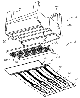
Figure 1 shows a three dimensional view, from above, of a printhead assembly,
in
accordance with the invention;
Figure 2 shows a three dimensional view, from below, of the assembly;
Figure 3 shows a three dimensional, exploded view of the assembly;
Figure 4 shows a bottom view of the assembly;
Figure 5 shows a three dimensional view, from below, of the assembly with
parts
omitted;
Figure 6 shows, on an enlarged scale, an end view of the assembly;
Figure 7 shows , on the enlarged scale, a sectional end view of the assembly:
Figure 8 shows a three dimensional, exploded view of a printhead module of the
assembly;
Figure 9 shows a bottom view of the module;
Figure 10 shows a plan view of the module;
Figure 11 shows a sectional end view of the module taken along line XI-XI in
Figure 10;
Figure 12 shows a three dimensional, exploded view of an ink reservoir of the
assembly;
Figure 13 shows a three dimensional view of a flexible printed circuit board
of the
assembly;
Figure 14 shows a three dimensional, exploded view of a busbar arrangement of
the
assembly;
Figure 15 shows a three dimensional view of a multiple printhead assembly
configuration; and
CA 02393049 2002-05-31
WO 01/42020 PCT/AUOO/01514
-3-
Figure 16 shows, on an enlarged scale, a sectional side view of the bonding of
the
printhead chip to the TAB film.
Detailed Description of the Drawings
A printhead assembly, in accordance with the invention is designated generally
by
the reference numeral 10. The assembly 10 uses a plurality of replaceable
printhead
modules 12. The advantage of this arrangement is the ability to easily remove
and replace
any defective modules 12 in the assembly 10. This eliminates having to scrap
an entire
printhead assembly 10 if only one module 12 is defective.
The assembly 10 comprises a chassis 14 on which an ink reservoir 16 is
secured. The
printhead modules 12 are, in turn, attached to the reservoir 16.
Each printhead module 12 is comprised of a microelectromechanical (Memjet)
chip
18 (shown most clearly in Figure 8 of the drawings) bonded by adhesive 20 to a
Tape
Automated Bond (TAB) film 22, the TAB film 22 being electrically connected to
the chip
18. The chip 18 and the TAB film 22 form a sub-assembly 24 which is attached
to a
micromolding 26. The micromolding 26 is, in turn, supported on a cover molding
28.
Each module 12 forms a sealed unit with four independent ink chambers 30
defined
in the cover molding 28, the ink chambers 30 supplying ink to the chip 18.
Each printhead
module 12 is plugged into a reservoir molding 32 (shown most clearly in
Figures 3 and 7 of
the drawings) of the ink reservoir 16 that supplies the ink. Ten modules 12
butt together
into the reservoir 16 to form a complete 8 inch printhead assembly 10. The ink
reservoirs 16
themselves are modular, so complete 8 inch printhead arrays can be configured
to form a
printhead assembly 10 of a desired width.
The 8 inch modular printhead assembly 10, according to the invention, is
designed
for a print speed and inkflow rate that allows up to 160 pages per minute
printing at 1600
dpi photographic quality. Additionally, a second printhead assembly, of the
same
construction, can be mounted in a printer on the opposite side for double
sided high speed
printing.
As described above, and as illustrated most clearly in Figure 8 of the
drawings, at the
heart of the printhead assembly 10 is the Memjet chip 18. The TAB film 22 is
bonded on to
the chip 18 and is sealed with the adhesive 20 around all edges of the chip 18
on both sides.
This forms the core Memjet printhead chip sub-assembly 24.
CA 02393049 2002-05-31
WO 01/42020 PCT/AUOO/01514
-4-
The sub-assembly 24 is bonded on to the micromolding 26. This molding 26 mates
with the TAB film 22 which, together, form a floor 34 (Figure 11) of the ink
chambers 30
of the cover molding 28. The chambers 30 open in a flared manner in a top 36
of the cover
molding 28 to define filling funnels 38. A soft elastomeric, hydrophobic
collar 40 is
arranged above each funnel 38. The collars 40 sealingly engage with
complementary filling
formations or nozzles 42 (Figure 7) of the reservoir molding 32 of the ink
reservoir 16 to
duct ink to the chip 18.
Snap details or clips 44 project from the top 36 of the cover molding 28 to
clip the
cover molding 28 releasably to the ink reservoir 16.
The TAB film 22 extends up an angled side wall 46 of the cover molding 28
where it
is also bonded in place. The side wal146 of the cover molding 28 provides the
TAB film
22 with a suitable bearing surface for data and power contact pads 48 (Figure
8).
The sub-assembly 24, the micromolding 26 and the cover molding 28 together
form
the Memjet printhead module 12. A plurality of these printhead modules 12 snap
fit in
angled, end-to-end relationship on to the ink reservoir 16. The reservoir 16
acts as a carrier
for the modules 12 and provides ink ducts 52 (Figure 7) for four ink colors,
Cyan, Magenta,
Yellow and blacK (CMYK). The four ink colors are channelled through the
individual
funnels 38 of the cover molding 28 into each printhead module 12.
The printhead modules 12 butt up to one another in an overlapping, angled
fashion
as illustrated most clearly in Figures 2 and 4 of the drawings. This is to
allow the Memjet
chips 18 to diagonally overlap in order to produce continuous printhead
lengths from 0.8
inches to 72 inches (for wide format printers) and beyond.
The Memjet chip 18 is 21.0 mm long x 0.54 mm wide and 0.3 mm high. A
protective silicon nozzle shield that is 0.3 mm high is bonded to the upper
surface of the
Memjet chip 18.
Each Memjet nozzle includes a thermoelastic actuator that is attached to a
moving nozzle
assembly. The actuator has two structurally independent layers of titanium
nitride (TiN) that
are attached to an anchor on the silicon substrate at one end and a silicon
nitride (nitride)
lever arm/nozzle assembly at the other end. The top TiN or "heater" layer
forms an
electrical circuit which is isolated from the ink by nitride. The moving
nozzle is positioned
over an ink supply channel that extends through the silicon substrate. The ink
supply
channel is fluidically sealed around the substrate holes periphery by a TiN
sealing rim. Ink
CA 02393049 2002-05-31
WO 01/42020 PCT/AUOO/01514
-5-
ejection is prevented between the TiN rim and the nitride nozzle assembly by
the action of
surface tension over a 1 micron gap.
A 1 microsecond 3V, 27 mA pulse (85 nanoJoules) is applied to the terminals of
the
heater layer, increasing the heater temperature by Joule heating. The
transient thermal field
causes an expansion of the heater layer that is structurally relieved by an
"out of plane"
deflection caused by the presence of the other TiN layer.
Deflection at the actuator tip is amplified by the lever arm and forces the
nozzle
assembly towards the silicon ink supply channel. The nozzle assembly's
movement
combines with the inertia and viscous drag of the ink in the supply channel to
generate a
positive pressure field that causes the ejection of a droplet.
Memjet actuation is caused by a transient thermal field. The passive TiN layer
only
heats up by thermal conduction after droplet ejection. Thermal energy
dissipates by thermal
conduction into the substrate and the ink, causing the actuator to return to
the 'at rest'
position. Thermal energy is dissipated away from the printhead chip by ejected
droplets.
The drop ejection process takes around 5 microseconds. The nozzle refills and
waste heat
diffuses within 20 microseconds allowing a 50 KHz drop ejection rate.
The Memjet chip 18 has 1600 nozzles per inch for each color. This allows true
1600
dpi color printing, resulting in full photographic image quality. A 21 mm CMYK
chip 18
has 5280 nozzles. Each nozzle has a shift register, a transfer register, an
enable gate, and a
drive transistor. Sixteen data connections drive the chip 18.
Some configurations of Memjet chips 18 require a nozzle shield. This nozzle
shield
is a micromachined silicon part which is wafer bonded to the front surface of
the wafer. It
protects the Memjet nozzles from foreign particles and contact with solid
objects and
allows the packaging operation to be high yield.
The TAB film 22 is a standard single sided TAB film comprised of polyimide and
copper layers. A slot accommodates the Memjet chip 18. The TAB film 22
includes gold
plated contact pads 48 that connect with a flexible printed circuit board
(PCB) 54 (Figure
13) of the assembly 10 and busbar contacts 56 (Figure 14) of busbars 58 and 60
of the
assembly 10 to get data and power respectively to the chip 18. Protruding bond
wires are
gold bumped, then bonded to bond pads of the Memjet chip 18.
The junction between the TAB film 22 and all the chip sidewalls has sealant
applied
to the front face in the first instance. The sub-assembly 24 is then turned
over and sealant is
applied to the rear junction. This is done to completely seal the chip 18 and
the TAB film
CA 02393049 2002-05-31
WO 01/42020 PCT/AU00/01514
-6-
22 together to protect electrical contact because the TAB film 22 forms the
floor 34 of the
ink chambers 30 in the printhead module 12.
The flexible PCB 54 is a single sided component that supplies the TAB films 22
of
each printhead module 12 with data connections through contact pads, which
interface with
corresponding contacts 48 on each TAB film 22. The flex PCB 54 is mounted in
abutting
relationship with the TAB film 22 along the angled sidewall 46 of the cover
molding 28.
The flex PCB 54 is maintained in electrical contact with the TAB film 22 of
each printhead
module 12 by means of a pressure pad 62 (Figure 7). The PCB 54 wraps
underneath and
along a correspondingly angled sidewall 64 of the ink reservoir molding 32 of
the ink
reservoir 16. The part of the PCB 54 against the sidewal164 carries a 62 pin
connector 66.
The sidewall 64 of the ink reservoir molding 32 of the ink reservoir 16 is
angled to
correspond with the sidewall 32 of the cover molding 16 so that, when the
printhead
module 12 is mated to the ink reservoir 16, the contacts 48 of the TAB film 22
wipe against
those of the PCB 54. The angle also allows for easy removal of the module 12.
The flex
PCB 54 is 'sprung' by the action of the deformable pressure pad 62 which
allows for
positive pressure to be applied and maintained between the contacts of the
flex PCB 54 and
the TAB film 22.
The micromolding 26 is a precision injection molding made of an Acetal type
material. It accommodates the Memjet chip 18 (with the TAB film 22 already
attached) and
mates with the cover molding 28.
Rib details 68 (Figure 8) in the underside of the micromolding 26 provide
support
for the TAB film 22 when they are bonded together. The TAB film 22 forms the
floor 34 of
the printhead module 12, as there is enough structural integrity due to the
pitch of the ribs
68 to support a flexible film. The edges of the TAB film 22 seal on the
underside walls of
the cover molding 28.
The chip 18 is bonded on to 100 micron wide ribs 70 that run the length of the
micromolding 26. A channel 72 is defined between the ribs 70 for providing the
final ink
feed into the nozzles of the Memjet chip 18.
The design of the micromolding 26 allows for a physical overlap of the Memjet
chips 18 when they are butted in a line. Because the Memjet chips 18 now form
a
continuous strip with a generous tolerance, they can be adjusted digitally to
produce the
required print pattern, rather than relying on very close tolerance moldings
and exotic
materials to perform the same function. The pitch of the modules 12 is 20.33
mm.
CA 02393049 2002-05-31
WO 01/42020 PCT/AUOO/01514
-7-
The micromolding 26 fits inside the cover molding 28, the micromolding 26
bonding on to a set of vertical ribs 74 extending from the top 36 of the cover
molding 28.
The cover molding 28 is a two shot, precision injection molding that combines
an
injected hard plastic body (Acetal) with soft elastomeric features (synthetic
rubber). This
molding interfaces with the sub-assembly 24 bonded to the micromolding 26.
When bonded
into place the base sub-assembly, comprising the sub-assembly 24 and the
micromolding
26, mates with the vertical ribs 74 of the cover molding 28 to form the sealed
ink chambers
30.
As indicated above, an opening of each chamber 30 is surrounded by one of the
collars 40. These soft collars 40 are made of a hydrophobic, elastomeric
compound that
seals against the ink nozzles 42 of the ink reservoir 16. The snap fits 44 on
the cover
molding 28 locate the module 12 with respect to the ink reservoir 16.
The ink reservoir 16 comprises the ink reservoir molding 32 and a lid molding
76
(Figure 7). The molding 32 is a simple four chamber injection molding with the
lid molding
76 that is bonded on top to form a sealed environment for each color ink. Ink
supply pipes
78 (Figure 12) are arranged at one end of the lid molding 76 to communicate
with ink
channels 80 defined in the reservoir molding 32. Labyrinthine, hydrophobic air
holes 82 are
defined at an opposed end of the lid molding 76. The air holes 82 are included
for bleeding
the channels 80 during charging. These holes 82 are covered over with a self
adhesive film
84 after charging.
The lid molding 76 has heat stakes 88, (pins that are designed to melt and
hold the
molding onto another part) which position and secure the ink reservoir 16 to
the punched,
sheet metal chassis 14. Additional heat stakes 90 are arranged along the
reservoir molding
32. These stakes are shown after deformation in Figure 1 of the drawings once
the ink
reservoir 16 has been secured to the chassis 14.
Receiving formations 92 are defined along the sides of the reservoir molding
32 for
releasably receiving the clips 44 of the printhead modules 12.
As previously described, the sidewall 64 on the side of the reservoir molding
32
provides a mounting area for the flexible PCB 54 and data connector 66. The
reservoir
molding 32 also carries details for facilitating the accurate mounting of the
V-and V+
busbars 58 and 60, respectively.
The metal chassis 14 is a precision punched, folded and plated metal chassis
used to
mount the printhead assembly 10 into various products. The ink reservoir 16 is
heat staked
CA 02393049 2002-05-31
WO 01/42020 PCT/AUOO/01514
-8-
to the chassis 14 via the heat stakes 88 and 90. The chassis 14 includes a
return edge 94 for
mechanical strength. The chassis 14 can be easily customized for printhead
mounting and
any further part additions. It can also be extended in length to provide
multiple arrays of
printhead assemblies 10 for wider format printers.
Slots 97 are defined in the chassis 14 for enabling access to be gained to the
clips 44
of the modules 12 to release the modules 12 from the ink reservoir 16 for
enabling
replacement of one or more of the modules 12.
Thin finger strip metallic strip busbars 58 and 60 conduct V- and V+,
respectively, to
the TAB film 22 on each printhead module 12. The two busbars 58 and 60 are
separated by
an insulating strip 96 (Figure 14). The flexible, finger-like contacts 56 are
arranged along
one side edge of each busbar 58, 60. The contacts 56 electrically engage the
relevant contact
pads 48 of the TAB film 22 of each module 12 for providing power to the module
12. The
contacts 56 are separated by fine rib details on the underside of the ink
reservoir molding
32.
A busbar sub-assembly 98, comprising the busbars 58, 60 and the insulating
strip 96
is mounted on the underside of the sidewa1164 of the reservoir molding 32 of
the ink
reservoir 16. The sub-assembly is held captive between that sidewall 64 and
the sidewall 46
of the cover molding 28 by the pressure pad 62.
A single spade connector 100 is fixed to a protrusion 102 on the busbar 58 for
ground. Two spade connectors 104 are mounted on corresponding protrusions 106
on the
busbar 60 for power. The arrangement is such that, when the sub-assembly 98 is
assembled,
the spade connectors 104 are arranged on opposite sides of the spade connector
100. In this
way, the likelihood of reversing polarity of the power supply to the assembly
10, when the
assembly 10 is installed, is reduced. During printhead module 12 installation
or
replacement, these are the first components to be disengaged, cutting power to
the module
12.
To assemble the printhead assembly 10, a Memjet chip 18 is dry tested in
flight by a
pick and place robot, which also dices the wafer and transports individual
chips 18 to a
TAB film bonding area. When a chip 18 has been accepted, a TAB film 22 is
picked,
bumped and applied to the chip 18.
A slot in the TAB film 22 that accepts the chip 18 and has the adhesive 20,
which
also functions as a sealant, applied to the upper and lower surfaces around
the chip 18 on all
CA 02393049 2002-05-31
WO 01/42020 PCT/AUOO/01514
-9-
sides. This operation forms a complete seal with the side walls of the chip
18. The
connecting wires are potted during this process.
The Memjet chip 18 and TAB film 22 sub-assembly 24 is transported to another
machine containing a stock of micromoldings 26 for placing and bonding.
Adhesive is
applied to the underside of the fine ribs 70 in the channel 72 of the
micromolding 26 and
the mating side of the underside ribs 68 that lie directly underneath the TAB
film 22. The
sub-assembly 24 is mated with the micromolding 26.
The micromolding sub-assembly, comprising the micromolding 26 and the sub-
assembly 24, is transported to a machine containing the cover moldings 28.
When the
micromolding sub-assembly and cover molding 28 are bonded together, the TAB
film 22 is
sealed on to the underside walls of the cover molding 28 to form a sealed
unit. The TAB
film 22 further wraps around and is glued to the sidewall 46 of the cover
molding 28.
The chip 18, TAB film 22, micromolding 26 and cover molding 28 assembly form a
complete Memjet printhead module 12 with four sealed independent ink chambers
30 and
ink inlets 38.
The ink reservoir molding 32 and the cover molding 76 are bonded together to
form
a complete sealed unit. The sealing film 84 is placed partially over the air
outlet holes 82 so
as not to completely seal the holes 82. Upon completion of the charging of ink
into the ink
reservoir 16, the holes 82 are sealed by the film 84. The ink reservoir 16 is
then placed and
heat staked on to the metal chassis 14.
The full length flexible PCB 54 with a cushioned adhesive backing is bonded to
the
angled sidewall 64 of the ink reservoir 16. The flex PCB 54 terminates in the
data connector
66, which is mounted on an external surface of the sidewall 64 of the ink
reservoir 16.
Actuator V- and V+ connections are transmitted to each module 12 by the two
identical metal finger strip busbars 58 and 60. The busbar sub-assembly 98 is
mounted
above the flex PCB 54 on the underside of the sidewall 64 of the ink reservoir
molding 32.
The busbars 58, 60 and the insulating strip 96 are located relative to the ink
reservoir
molding 32 via pins (not shown) projecting from the sidewall 64 of the ink
reservoir
molding 32, the pins being received through locating holes 108 in the busbars
58, 60 and
the insulating strip 96.
The Memjet printhead modules 12 are clipped into the overhead ink reservoir
molding 32. Accurate alignment of the module 12 to the reservoir molding 32 is
not
CA 02393049 2002-05-31
WO 01/42020 PCT/AUOO/01514
-10-
necessary, as a complete printhead assembly 10 will undergo digital adjustment
of each chip
18 during final QA testing.
Each printhead module's TAB film 22 interfaces with the flex PCB 54 and
busbars
58, 60 as it is clipped into the ink reservoir 16. To disengage a printhead
module 12 from
the reservoir 16, a custom tool is inserted through the appropriate slots 97
in the metal
chassis 14 from above. The tool 'fingers' slide down the walls of the ink
reservoir molding
32, where they contact the clips 44 of the cover molding 28. Further pressure
acts to ramp
the four clips 44 out of engagement with the receiving formations 92 and
disengage the
printhead module 12 from the ink reservoir 16.
To charge the ink reservoir 16 with ink, hoses 110 ( Figure 3) are attached to
the
pipes 78 and filtered ink from a supply is charged into each channel 80. The
openings 82 at
the other end of the ink reservoir cover molding 76 are used to bleed off air
during priming.
The openings 82 have tortuous ink paths that run across the surface, which
connect through
to the internal ink channels 80. These ink paths are partially sealed by the
bonded
transparent plastic film 84 during charging. The film 84 serves to indicate
when inks are in
the ink channels 80, so they can be fully capped off when charging has been
completed.
For electrical connections and testing, power and data connections are made to
the
flexible PCB 54. Final testing then commences to calibrate the printhead
modules 12. Upon
successful completion of the testing, the Memjet printhead assembly 10 has a
plastic sealing
film applied over the underside that caps the printhead modules 12 and, more
particularly,
their chips 18, until product installation.
It is to be noted that there is an overlap between adjacent modules 12. Part
of the
testing procedure determines which nozzles of the overlapping portions of the
adjacent
chips 18 are to be used.
As shown in Figure 15 of the drawings, the design of the modular Memjet
printhead
assemblies 10 allows them to be butted together in an end-to-end
configuration. It is
therefore possible to build a multiple printhead system 112 in, effectively,
unlimited
lengths. As long as each printhead assembly 10 is fed with ink, then it is
entirely possible to
consider printhead widths of several hundred feet. This means that the only
width limit for a
Memjet printer product is the maximum manufacturable size of the intended
print media.
Figure 15 shows how a multiple Memjet printhead system 112 could be configured
for wide format printers. Replaceable ink cartridges 114, one for each color,
are inserted
into an intermediate ink reservoir 116 that always has a supply of filtered
ink. Hoses 118
CA 02393049 2002-05-31
WO 01/42020 PCT/AUOO/01514
-11-
exit from the underside of the reservoir 118 and connect up to the ink inlet
pipes 78 of each
printhead assembly 10.
It will be appreciated by persons skilled in the art that numerous variations
and/or
modifications may be made to the invention as shown in the specific
embodiments without
departing from the spirit or scope of the invention as broadly described. The
present
embodiments are, therefore, to be considered in all respects as illustrative
and not
restrictive.