Note: Descriptions are shown in the official language in which they were submitted.
CA 02394895 2002-06-19
WO 01/47044
PCT/GB00/04940
FORMING INTERCONNECTS
This invention relates to forming interconnects, especially by solution
processing.
Semiconducting conjugated polymer thin-film transistors (TFTs) have recently
become of interest for applications in cheap, logic circuits integrated on
plastic
substrates (C. Drury, et al., APL 73, 108 (1998)) and optoelectronic
integrated
devices and pixel transistor switches in high-resolution active-matrix
displays (H.
Sirringhaus, et al., Science 280, 1741 (1998), A. Dodabalapur, et al. Appl.
Phys.
Lett. 73, 142 (1998)). In test device configurations with a polymer
semiconductor
and inorganic metal electrodes and gate dielectric layers high-performance
TFTs
have been demonstrated. Charge carrier mobilities up to 0.1 cm2/Vs and ON-OFF
current ratios of 106-108 have been reached, which is comparable to the
performancé of amorphous silicon TFTs (H. Sirringhaus, et al., Advances in
Solid
State Physics 39, 101 (1999)).
Thin, device-quality films of conjugated polymer semiconductors can be formed
by
coating a solution of the polymer in an organic solvent onto the substrate.
The
technology is therefore ideally suited for cheap, large-area solution
processing
compatible with flexible, plastic substrates. To make full use of the
potential cost
and ease of processing advantages it is desirable that all components of the
devices including the semiconducting layers, the dielectric layers as well as
the
conducting electrodes and interconnects are deposited from solution.
To fabricate all-polymer TFT devices and circuits the following main problems
have to be overcome:
- Integrity of multilayer structure: During solution deposition of subsequent
semiconducting, insulating and/or conducting layers the underlying layers
should not be dissolved, or swelled by the solvent used for the deposition of
the subsequent layers. Swelling occurs if solvent is incorporated into the
CA 02394895 2011-04-06
2
underlying layer which usually results in a degradation of the
properties of the layer.
High-resolution patterning of electrodes: The conducting layers need
to be patterned to form well-defined interconnects and TFT channels
with channel lengths L 10 pm.
To fabricate TFT circuits vertical interconnect areas (via holes) need
to be formed to electrically connect electrodes in different layers of
the device.
In WO 99/10939 A2 a method to fabricate an all-polymer TFT is
demonstrated that relies on the conversion of the solution-processed layers
of the device into an insoluble form prior to the deposition of subsequent
layers of the device. This overcomes the problems of dissolution and
swelling of underlying layers. However, it severely limits the choice of
semiconducting materials, that can be used, to the small and in several
respects undesirable class of precursor polymers. Furthermore, cross-
linking of the dielectric gate insulating layer makes the fabrication of via-
holes through the dielectric layers difficult, such that techniques such as
mechanical punching are used (WO 99/10939 A1).
SUMMARY OF THE INVENTION
In accordance with one aspect of the invention, there is provided a method
for forming an electronic device. The method involves forming a first
conductive or semiconductive layer, forming a sequence of at least one
insulating layer and at least one semiconducting layer over the first
conductive or semiconductive layer, locally depositing solvents at a
localised region of the sequence so as to dissolve the sequence of
insulating and semiconducting layers in the region to leave a void
extending through the sequence of layers, wherein material dissolved to
form said void is redeposited at the side of said void, and depositing
conductive or semiconductive material in the void.
CA 02394895 2012-05-22
3
Locally depositing solvents may be done using a printing technique.
The solvents may be deposited simultaneously. Alternatively the solvents
may be deposited sequentially.
In accordance with another aspect of the invention, there is provided a
method for forming an electronic device. The method involves forming a
first conductive or semiconductive layer, forming a soluble insulating layer
over the first conductive or semiconductive layer, locally depositing a
solvent at a localised region of the insulating layer so as to dissolve the
insulating layer in the region to leave a void extending through the
insulating layer, wherein material dissolved to form said void is redeposited
at the side of said void, and depositing conductive or semiconductive
material in the void.
Locally depositing the solvent may be done using a printing technique.
The first layer may be substantially insoluble in the solvent or solvents.
The first layer may comprise a semiconductive conjugated polymer.
The first layer may comprise F8T2 or TFB.
The first layer may be an active layer of the electronic device.
The method may further involve depositing a conductive layer under the
first layer.
The conductive layer may be an electrode of the electronic device.
The first layer may comprise a conductive conjugated polymer.
CA 02394895 2009-09-09
4
The volume of the solvent or solvents may be greater than that required to
dissolve the sequence of insulating and semiconducting layers or the
soluble insulating layer in the region.
The method may further involve forming a further conductive or
semiconductive layer over the sequence of insulating and semiconducting
layers or the insulating layer and in contact with the material in the void
The first conductive or semiconductive layer may form an electrode or an
interconnect.
The further conductive or semiconductive layer may form an electrode or
an interconnect.
The solvent or solvents may be deposited by ink-jet printing.
The solvent or solvents may be deposited as a single droplet by ink-jet
printing.
The solvent or solvents may be deposited as a plurality of droplets by ink-
jet printing.
The boiling point of the solvent or of the solvents in combination may be
greater than 80 C.
The boiling point of the solvent or of the solvents in combination may be
greater than 100 C.
The boiling point of the solvent or of the solvents in combination may be
less than 100 C.
Each of the layers may have a solubility greater than 1 weight percent per
volume in one or more of the solvents.
Each of the layers may have a solubility greater than 2 weight percent per
volume in one or more of the solvents.
CA 02394895 2012-05-22
The first insulating layer may have a solubility greater than 1 weight percent
per volume in the solvent.
The first insulating layer may have a solubility greater than 2 weight percent
per volume in the solvent.
The volume of deposited solvent may be less than 50 pl.
The volume of deposited solvent may be less than 20 pl.
The volume of deposited solvent may be less than 5 pl.
The contact angle of the deposited solvent on the layer or sequence of
layers to be dissolved may be larger than 5 , but less than 90 .
The contact angle of the deposited solvent on the layer or sequence of
layers to be dissolved may be larger than 20 , but less than 90 .
The contact angle of the deposited solvent on the layer or sequence of
layers to be dissolved may be larger than 50 , but less than 90 .
The layer or sequence of layers to be dissolved may have been treated in
order to provide a greater repellence for droplets of the deposited solvent
or solvents.
The surface treatment may be provided by deposition of a self-assembled
monolayer.
The electronic device may be a transistor and the material deposited in the
void forms a via hole interconnect between electrodes and/or interconnect
lines in different layers of the device.
The solvent or one of the solvents may be an alcohol.
The solvent or one of the solvents may be IPA or methanol.
The method may further involve forming a confinement structure for
confining the solvent or solvents to the localised region by means of its
wetting properties.
CA 02394895 2012-05-22
6
The confinement structure may be provided by a self-assembled
monolayer.
In accordance with another aspect of the invention, there is provided a
method for forming an electronic device. The method involves forming a
first conductive or semiconductive layer, forming a sequence of insulating
and semiconducting layers over the first conductive or semiconductive
layer, and using a printing technique to locally deposit a diffusive dopant
from solution at a localised region of the sequence so as to modify the
insulating and semiconducting layers in the region and thereby form a
channel of electrically conductive material extending through the sequence
of layers.
The diffusive dopant may be deposited by ink-jet printing.
The electronic device may be a transistor and the channel forms a via hole
interconnect between electrodes and/or interconnect lines in different
layers of the device.
Locally depositing a diffusive dopant may be done using a printing
technique.
The insulating layer may comprise PVP.
One of the insulating layer and a layer directly underlying it may be soluble
in a polar solvent and the other of the insulating layer and the layer
directly
underlying it is soluble in a non-polar solvent.
According to a further aspect of the present invention there is provided an
electronic device formed by a method as set out above.
According to a further aspect of the present invention there is provided a
logic circuit, display or memory device comprising a plurality of devices as
set out above.
CA 02394895 2009-09-09
=
6a
According to a further aspect of the present invention there is provided a
logic circuit comprising a plurality of such devices interconnected so as to
perform a logical function.
At least a first one of the devices may be connected to another of the
devices by means of conductive material located in a void formed through
at least one layer of the first one of the devices.
The display device may comprise an optically active region switchable by
such an electronic device, the electronic device being coupled to the
optically active region by means of conductive material located in a void
formed through at least one layer of the device.
According to a further aspect of the present invention there is provided an
electronic device having a plurality of dielectric layers and being formed by
a method as set out above so as to have a void through at least one of the
dielectric layers, the device comprising layers of interconnects spaced
apart by the said one of the dielectric layers, wherein at least one of the
interconnects in one layer is electrically connected to an interconnect in
another layer by means of conductive material located in the void.
The present invention will now be described by way of example, with
reference to the accompanying drawings, in which:
figure 1 shows different device configurations of solution processed,
all-polymer TFTs;
figure 2 shows transfer characteristics of polymer TFTs according to
Fig. lc with a F8T2 active layer, a PVP gate insulating layer, and a
PEDOT/PSS gate electrode;
figure 3 shows transfer characteristics of polymer TFTs according to
Fig. lc with a F8T2 active layer, a PVP gate insulating layer, and a
PEDOT/PSS gate
CA 02394895 2002-06-19
WO 01/47044
PCT/GB00/04940
7
electrodes deposited with the sample held at room temperature (a) and
approximately 50 C (b).
figure 4 shows output (a) and transfer characteristics (b) of a F8T2 all-
polymer TFT containing a F8 diffusion barrier and a PVP surface modification
layer as in figure 1(a);
figure 5 shows transfer characteristics of F8T2 all-polymer TFTs as in
figure 1(a) with a TFB (a) and polystyrene (b) diffusion barrier and a PVP
surface
modification layer;
figure 6 shows an optical micrograph of an all-polymer TFT according to
figure 1(a) with an F8T2 active layer and source-drain electrodes printed
directly
onto a bare glass substrate;
figure 7 shows the fabrication of TFTs with small channel length and small
overlap capacitance through patterning of the substrate surface into
hydrophobic
and hydrophilic areas;
figure 8 shows optical micrographs of the channel region of transistors with
L = 20 pm (a) and L = 5 pm (b) after UP deposition of PEDOT/PSS source/drain
electrodes in the vicinity of a hydrophobic polyimide bank;
Figure 9 shows optical micrographs taken during the deposition of ink
droplets in the vicinity of a polyimide bank.
figures 10 and 11 show output and transfer characteristics of transistors
formed as in figure 7(c) and having channel lengths L = 20 pm and 7 pm
respectively;
figure 12 shows a schematic diagram (a) Dektak profilometry and optical
micrographs (b) of the process of forming via holes by successive deposition
of
methanol droplets onto a 1.3 pm thick PVP gate dielectric layer and (c)
dependence of the via-hole outer and inner diameter on the diameter of the
inkjet
droplets and the thickness of the PVP layer;
figure 13 shows the current-voltage characteristics through a via hole with
a bottom PEDOT electrode and a top electrode.
figure 14 illustrates different processes to fabricate via-holes;
CA 02394895 2009-09-09
8
figure 15 shows applications of via holes such as logic inverters
(depletion-load (a), enhancement-load (b) and resistance-load (c)), and
multilevel interconnect schemes (d);
figure 16 shows the characteristics of enhancement-load inverter
circuits as in figure 1(a) fabricated with printed all-polymer TFTs with
different
ratios of the sizes W/L of the two transistors;
figure 17 shows an alternative bottom-gate device configuration; and
figure 18 shows a schematic drawing of an active matrix pixel in which
the display or memory element is controlled by a voltage (a) or a current (b).
Preferred fabrication methods described herein permit the fabrication of an
all-
organic, solution-processed thin-film transistor, in which none of the layers
is
converted or cross-linked into an insoluble form. Each layer of such a device
may remain in a form that is soluble in the solvent from which it was
deposited. As will be described in more detail below, this enables a simple
way of fabricating via-holes through dielectric insulating layers based on
local
deposition of solvents. Such a device may, for example, comprise one or
more of the following components:
patterned conducting source-drain and gate electrodes and
interconnects.
a semiconducting layer with a charge carrier mobility exceeding 0.01
cm2Ns and a high ON-OFF current switching ratio exceeding 104.
a thin gate insulating layer.
CA 02394895 2002-06-19
WO 01/47044
PCT/GB00/04940
9
- a diffusion barrier layer that protects the semiconducting layer and the
insulating layer against unintentional doping by impurities and ionic
diffusion.
- a surface modification layer that enables high-resolution patterning
of the
gate electrode by printing techniques.
- via-holes for interconnects through dielectric layers.
However, it will be appreciated that the methods described herein are not
limited
to the fabrication of devices having all the features set out above.
The fabrication of a first illustrative device will now be described with
reference to
figure 1. The device of figure 1 is a thin-film field effect transistor (TFT)
configured
to have a top-gate structure.
On top of a cleaned 7059 glass substrate 1 source-drain electrodes 2, 3 and
interconnect lines between the electrodes and the contact pads (not shown) are
deposited by ink-jet printing a solution of the conducting polymer
polyethylenedioxythiophene/polystyrolsulfonate (PEDOT (0.5 weight %) / PSS
(0.8 weight %)) in water. Other solvents such as methanol, ethanol,
isopropanol or
acetone may be added to affect surface tension, viscosity and wetting
properties
of the ink. PEDOT/PSS is obtained commercially from Bayer (available as
"Baytron P"). The IJP printer is of the piezoelectric type. It is equipped
with a
precision two-dimensional translation stage and a microscope stage enabling
the
alignment of subsequently printed patterns with respect to each other. The IJP
head is driven with a voltage pulse. Suitable drive conditions to eject
droplets of a
typical solid content of 0.4 ng per droplet are achieved with a pulse height
of 20V,
rise time of 10 /JS, and a fall time of 10 ps. After drying on the glass
substrate
they produce a PEDOT dot with a typical diameter of 50 pm, and typical
thickness
of 500 A.
The IJP of the source-drain electrodes is performed in air. Afterwards the
samples
are transferred to an inert atmosphere glove box system. The substrates are
then
CA 02394895 2002-06-19
WO 01/47044
PCT/GB00/04940
spun-dried in the organic solvent that will later be used for the deposition
of the
active semiconducting layer, such as mixed xylenes in the case of polyfluorene
polymers. They are then annealed for 20 minutes at 200 C in inert nitrogen
atmosphere to remove residual solvent and other volatile species in the
PEDOT/PSS electrodes. Then a 200-1000 A thick film of the active
semiconducting polymer 4 is deposited by spin-coating. Various semiconducting
polymers have been used such as regioregular poly-3-hexylthiophene (P3HT),
and polyfluorene co-polymers such as poly-9,9'-dioctylfluorene-co-dithiophene
(F8T2). F8T2 is a preferred choice as it exhibits good stability in air during
the
deposition of the gate electrode in air. A 5-10 mg/ml solution of F8T2 in
anhydrous, mixed xylenes (purchased from Romil) is spin-coated at 1500-2000
rpm. In the case of P3HT a 1 weight % solution in mixed xylene was used. The
underlying PEDOT electrodes are insoluble in a non-polar organic solvent such
as
xylene. The films are then spun-dried in the solvent that will later be used
for the
deposition of the gate insulator layer 5, such as isopropanol or methanol.
A subsequent annealing step can then be performed to enhance the charge
transport properties of the semiconducting polymer. For polymers that exhibit
a
liquid crystalline phase at elevated temperatures annealing at a temperature
above the liquid-crystalline transition results in orientation of the polymer
chains
parallel to each other. In the case of F8T2, annealing is performed at 275-285
C
for 5-20 min under inert N2 atmosphere. The samples are then rapidly quenched
to room temperature to freeze in the orientation of the chains and produce an
amorphous glass. If samples are prepared on plain glass substrates without an
alignment layer the polymer adopts a multidomain configuration in which
several
liquid-crystalline domains with random orientation are located within the TFT
channel. Transistor devices in which the F8T2 is prepared in a glassy state by
quenching from a liquid-crystalline phase exhibit mobilities on the order of 5-
10-3
cm2Ns, that are by more than an order of magnitude higher than mobilities
measured on devices with as-spun F8T2 films. As-deposited devices also exhibit
CA 02394895 2002-06-19
WO 01/47044
PCT/GB00/04940
11
higher turn-on voltages Vo. This is attributed to a lower density of localized
electronic trap states in the glassy phase compared to the as-deposited phase,
that is partially crystalline.
Further improvements of the mobility by typically a factor of 3-5 can be
obtained if
the polymer is prepared in a monodomain state with uniaxial alignment of the
polymer chains parallel to the transistor channel. This can be achieved by
coating
the glass substrate with a suitable alignment layer, such as a mechanically
rubbed
polyimide layer (9 in figure 1(b)). In the monodomain state the polymer chains
are
aligned uniaxially parallel to the rubbing direction of the underlying
polyimide
layer. This results in a further enhancement of charge carrier mobility in
devices in
which the TFT channel is parallel to the alignment direction of the chains.
Such a
process is described in more detail in our co-pending UK patent application
number 9914489.1.
After deposition of the semiconductor layer, the gate insulating layer 5 is
deposited by spin-coating a solution of polyhydroxystyrene (also-called
polyvinylphenol (PVP)) from a polar solvent in which the underlying
semiconducting polymer is not soluble. A preferred choice of solvents are
alcohols
such as methanol, 2-propanol or butanol, in which non-polar polymers such as
F8T2 have exceptionally low solubility and do not swell. The thickness of the
gate
insulating layer is between 300 nm (solution concentration 30 mg/m1) and 1.3
pm
(solution concentration 100 mg/ml). Other insulating polymers and solvents
that
satisfy the solubility requirements such as poly-vinylalcohol (PVA) in water
or
poly-methyl-methacrylate (PMMA) in butyl acetate or propylene glycol methyl
ether acetate may also be used.
The gate electrode 6 is then deposited over the gate insulating layer. The
gate
electrode layer may be deposited directly over the gate insulating layer (see
figure
1(c)) or there may be one or more intermediate layers (see figure 1(a) and
(b)), for
CA 02394895 2002-06-19
WO 01/47044
PCT/GB00/04940
12
example for surface modification, diffusion barrier or process reasons such as
solvent compatibility.
To form the simpler device of figure 1(c) a PEDOT/PSS gate 6 may be printed
directly on top of the PVP insulating layer 5. The substrate is transferred to
the
IJP station in air again where a PEDOT/PSS gate electrode pattern is printed
from
a water solution. The underlying PVP gate insulating layer has a low
solubility in
water such that the integrity of the gate dielectric is preserved during the
printing
of the PEDOT/PSS gate electrode. Although PVP contains a large density of
polar
hydroxyl groups, its solubility in water is low because of the very non-polar
polystyrene-like backbone. Similarly PMMA is insoluble in water. Figure 2
shows
the transfer characteristics of an IJP TFT with a F8T2 semiconducting layer, a
PVP gate insulating layer, and IJP PEDOT/PSS source-drain and gate electrodes.
The device characteristics are measured under nitrogen atmosphere. Consecutive
measurements are shown with increasing (upward triangles) and decreasing
(downward triangles) gate voltage, respectively. The characteristics belong to
devices made from a freshly prepared batch (a) and a one-year old batch (b) of
PEDOT/PSS (Baytron P). Transistor action can clearly be seen, however, the
devices exhibit an unusual normally-on behaviour with Positive threshold
voltages
Vo>10V, whereas reference devices fabricated with evaporated gold source-drain
and gate electrodes were found to exhibit normally off behaviour (Vo < 0). In
devices formed from the "old" batch of PEDOT (figure 2(b)) large hysteresis
effects were observed which are attributed to high concentration of mobile
ionic
impurities (see below). If the sweep is started in deep depletion (Vg=+40V),
the
transistor turns on at Vfo +20V (upward triangles). However, on the reverse
scan (downward triangles) the transistor only turns off at \i ro > +35V.
The normally-on behaviour and the hysteresis effects are likely to be caused
by
the diffusion of ionic species in one of the layers of the device. The
unusually
large positive values of Vo suggest that the ion is negative. A positive
species
CA 02394895 2002-06-19
WO 01/47044
PCT/GB00/04940
13
would be expected to compensate some of the mobile charge in the accumulation
layer and lead to a shift of Vo to more negative values. To identify the
origin of
this ionic species devices were fabricated in which the top-gate IJP PEDOT
electrode was replaced by an evaporated gold electrode while the other layers
and the PEDOT source/drain electrodes were fabricated as described above. It
was found that in this configuration the devices are normally-off and exhibit
stable
threshold voltages. This implies that the doping and hysteresis effects in the
all-
polymer device are related to the solution deposition of the conducting
polymer
top gate electrode, and the possible diffusion of mobile, ionic impurities
from the
PEDOT solution/film into the underlying layers of the device.
It was found to be possible to control the value of the threshold voltage and
to
reduce the amount of hysteresis by depositing the gate electrode onto a heated
substrate. This reduces the drying time of the droplet on the substrate. Fig.
3(b)
shows the transfer characteristics of a TFT device for which the substrate was
heated to a temperature of 50 C during deposition of the gate electrode. It
can be
seen that the hysteresis effect is much smaller than for gate deposition at
room
temperature (Fig. 3b), and that Vo has a relatively small positive value of
6V. By
controlling the deposition temperature the threshold voltage can be adjusted
in a
range of Vo = 1-20V.
Devices with gate electrodes deposited directly onto the PVP layer as in
figure
1(c) are of the depletion-type. This normally-on behaviour is useful for
depletion-
type logic circuits such as the simple depletion-load logic inverter (figure
14(a)).
To fabricate enhancement-type, normally-off TFTs the doping of the
semiconductor during the deposition of the gate can be prevented by
incorporation of a diffusion barrier layer. In the device of figure 1(a) and
(b) a thin
layer 7 of a non-polar polymer is deposited on top of the PVP gate insulating
layer
prior to the deposition of the conducting polymer gate electrode. This layer
is
CA 02394895 2002-06-19
WO 01/47044
PCT/GB00/04940
14
believed to act as diffusion barrier blocking the diffusion of ionic species
through
the moderately polar PVP insulator. PVP contains a high density of polar
hydroxyl
groups which tend to enhance the conductivity and diffusivity of ions through
the
film. Several non-polar polymers have been used such as poly-9,9'-
dioctylfluorene
(F8), polystyrene (PS),
poly(9,9'-dioctyl-fluorene-co-N-(4-butylphenyl)
diphenylamine) (TFB) or F8T2. Thin films of these polymers on the order of 50-
100nm can be deposited on the surface of the PVP gate insulating layer from a
solution in a non-polar organic solvent such as xylene, in which PVP is
insoluble.
Direct printing of PEDOT/PSS from a polar solution in water on top of the non-
polar diffusion barrier layer or on top of a moderately polar polymer such as
PMMA has been found to be problematic because of poor wetting and large
contact angles. To address this, a surface modification layer 8 is deposited
on top
of the non-polar polymer. This
layer provides a hydrophilic rather than
hydrophobic surface on to which the PEDOT/PSS may more readily be formed.
This permits enables high-resolution printing of the gate electrode pattern.
To
form the surface modification layer a thin layer of PVP can be deposited from
isopropanol solution, in which the underlying diffusion barrier layer is
insoluble.
The thickness of the PVP layer is preferably less than 50 nm. High-resolution
printing of PEDOT/PSS is possible on the surface of PVP. Alternative surface
modification layers may be used. These include thin layers of soap-like
surfactants or polymers containing a hydrophilic and a hydrophobic functional
group. These molecules would tend to phase-separate with the hydrophobic and
hydrophilic groups being attracted towards the interface with the underlying
non-
polar polymer and the free surface, respectively. Another possibility is the
brief
exposure of the surface of the non-polar diffusion barrier to a mild 02 plasma
rendering the surface hydrophilic. A suitable plasma treatment that does not
degrade the TFT device performance is exposure to a 13.5 MHz 02 plasma with a
power of 50 W for 12 s.
CA 02394895 2002-06-19
WO 01/47044
PCT/GB00/04940
A surface modification layer on top of the non-polar diffusion barrier may not
be
required if the gate electrode is printed from a solvent that is less polar
than water
such as formulation containing alcohols (isopropanol, methanol etc.).
The integrity of the layer sequence relies on the alternating deposition of
polymer
materials from polar and non-polar solvents. It is desirable that the
solubility of a
first layer in the solvent used for the deposition of a second layer is less
than 0.1%
weight per volume, preferably less than 0.01% weight per volume.
The criterion for solvent compatibility may be quantified using the Hildebrand
solubility parameters by which the degree of polarity can be quantified (D.W.
van
Krevelen, Properties of polymers, Elsevier, Amsterdam (1990)). The solubility
behaviour of each polymer (solvent) is described by three characteristic
parameters Eld, Op, ph, characterising the degree of dispersive interactions,
polar,
and hydrogen bonding interactions between polymer (solvent) molecules in the
liquid state. Values for these parameters can be calculated if the molecular
structure is known by adding contributions from the different functional
groups of
the polymer. They are tabulated for most common polymers. Often Op and D.dare
combined to Ev2F d2.+0102.
The free energy of mixing is given by OG,õ = OHm - T.DSm, where =OSm>0 is the
entropy of mixing and EJHm = V. (l)p= ii)s = auvP:Dvs)24:(0hP._¨hs=2
) ). (V: volume; (1)13, (1)S:
volume fraction of polymer (P) /solvent (S) in the mixture). From this it is
expected
that a polymer (P) is the more soluble in a solvent (S) the smaller OFIm,
i.e., the
smaller D = ((ovp._0,$)2+.(ohp._ohs)2.1/2.
) As an
approximate criterion, if the
interaction parameter D is smaller than approximately 5 the polymer is soluble
in
the solvent. If D is between 5-10, swelling is often observed. If D is larger
than 10,
the polymer is substantially insoluble in the solvent, and no swelling occurs.
In order to obtain sufficiently abrupt interfaces in a solution-processed TFT
device
it is therefore desirable that the respective D values for each of the polymer
layers
and the solvent of the next layer should be larger than approximately 10. This
is
CA 02394895 2002-06-19
WO 01/47044
PCT/GB00/04940
16
particularly important for the semiconducting polymer layer and the solvent of
the
gate dielectric. In the case of F8T2 and isopropanol (butyl acetate) we
estimate D
to be approximately 16 (12).
For some device configurations the entire multilayer structure may be built up
by
an alternating sequence of polymers that contain mainly polar groups and are
soluble in a highly polar solvent such as water, and polymers that contain
only a
few or do not contain any polar groups and are soluble in a non-polar solvent,
such as xylene. In .this case the interaction parameter D is large because of
the
differences of II p for the polymer layer and solvent of the next layer. An
example
would be a transistor device comprising a highly polar source-drain electrode
of
PEDOT/PSS, a non-polar semiconducting layer such as F8T2, a highly-polar gate
dielectric layer such as a polyvinylalcohol deposited from water solution, a
non-
polar diffusion barrier layer of TFB that also acts as a buffer layer to allow
the
deposition of the layer sequence, and a PEDOT/PSS gate electrode.
However, it is often convenient to have a non-polar semiconducting layer and a
polar gate electrode layer separated by a single dielectric layer. This layer
sequence is also possible by using a moderately polar polymer layer deposited
from a moderately polar solvent sandwiched between the highly polar and non-
polar polymer layer. . A moderately polar polymer is a polymer that contains
both
polar and non-polar groups, and is substantially insoluble in a highly polar
solvent.
Analogously, a moderately polar solvent contains both polar and non-polar
groups, but does not substantially dissolve a non-polar polymer. In terms of
the
solubility parameters a moderately polar solvent may be defined as one where
the
solubility parameter Oh is largely different from that of the underlying
polymer. In
this case swelling may be avoided (large D) even if the polar solubility
parameter
Op MO of the solvent may be similar to that of the underlying polymer layer.
The
moderately polar polymer may contain a specific functional group such as a
hydroxyl group that makes it soluble in a solvent containing a functional
group that
is attracted to the functional group of the polymer. This attraction may be a
CA 02394895 2002-06-19
WO 01/47044
PCT/GB00/04940
17
hydrogen bonding interaction. This functionality of the polymer may be used to
enhance its solubility in a moderately polar solvent and decrease its
solubility in a
polar solvent. An example of a moderately polar polymer is a PVP gate
dielectric
layer sandwiched between a non-polar semiconductor layer and a PEDOT/PSS
gate electrode layer (Fig. 1 c). An example of a moderately polar solvent is
an
alkylalcohol such as IPA (Oh = 8; F8T2: Oh %z-', 0).
Figure 4 shows the output (a) and transfer (b) characteristics of an all-
polymer
F8T2 IJP TFT with a PVP gate insulator layer, a F8 diffusion barrier layer and
a
PVP surface modification layer, as illustrated in figure 1(a) (L = 50 pm). The
device exhibits clean, near-ideal normally -off transistor action with turn-on
at Vo
OV. The threshold voltage shift between upward (upward triangles) and downward
(downward triangles) voltage sweeps is IV. The device characteristics are very
similar to those of standard devices fabricated under inert atmosphere
conditions
with Au source-drain and gate electrodes. The field effect-mobility is on the
order
of 0.005-0.01 cm2Ns and the ON-OFF current ratio measured between Vg=0 and
-60V is on the order of 104-105.
Devices have been fabricated with a broad range of non-polar diffusion barrier
layers, such as F8, TFB (figure 5(a) shows transfer characteristics), PS
(figure
5(b) shows transfer characteristics), and F8T2. In each case clean normally-
off
behaviour and small hysteresis effects and threshold voltage shifts were
observed, which were of the same order of magnitude as those of reference
devices with gold source-drain electrodes. This supported the interpretation
that
insertion of a non-polar polymer below the gate electrode blocks diffusion of
ionic
impurities during and after the solution deposition of the gate insulating
layer.
This has been found to result in reproducible TFT threshold voltages and good
operating stability.
CA 02394895 2002-06-19
WO 01/47044
PCT/GB00/04940
18
Normally-off devices containing a diffusion barrier are preferred compared to
the
depletion-type device described above, since it is expected that the former
exhibit
better long term threshold voltage stability and better lifetime due to
suppression
of ionic diffusion.
For the semiconducting layer any solution processible conjugated polymeric or
oligomeric material that exhibits adequate field-effect mobilities exceeding
10-3
cm2/Vs, preferably exceeding 10-2 cm2Ns, may be used. Suitable materials are
reviewed for example in H.E. Katz, J. Mater. Chem. 7, 369 (1997), or Z. Bao,
Advanced Materials 12, 227 (2000).
One of the important requirements to fabricate printed TFTs with good
stability
and high ON-OFF current ratio is good stability of the semiconducting material
against unintentional doping by atmospheric oxygen and water during the
processing and printing steps. Printed TFTs have been fabricated with a range
of
semiconducting polymers as the active semiconducting layer, such as F8T2 (see
above), or regioregular P3HT deposited from mixed xylene solution. In the case
of P3HT TFTs prepared in test device configurations under inert atmosphere the
field-effect mobility of 0.05-0.1 cm2/Vs is somewhat higher than in the case
of
F8T2. However, regioregular P3HT is unstable against doping by oxygen and/or
water, resulting in an increase of the film conductivity during the printing
steps in
air and poor ON-OFF current ratio. This is related to the relatively low
ionisation
potential of P3HT, lp .===== 4.9 eV. High ON-OFF current ratios of >106 have
been
demonstrated for P3HT, but this requires a reductive dedoping step after the
deposition, such as exposure to hydrazine vapour (H. Sirringhaus, et al.,
Advances in Solid State Physics 39, 101 (1999)). However, on the IJP TFTs
described above this reductive post-processing step cannot be performed since
it
would also result in dedoping of the PEDOT electrodes and reduce their
conductivity significantly. Therefore, to achieve high current switching
ratios it is
CA 02394895 2002-06-19
WO 01/47044
PCT/GB00/04940
19
important that a polymer semiconductor is used with good stability against
unintentional doping by oxygen or water.
" A preferred class of materials to achieve good environmental stability and
high
mobility are A-B rigid-rod block-copolymers containing a regular ordered
sequence of A and B blocks. Suitable A blocks are structurally well defined,
ladder
type moieties with a high band gap, that have high ionisation potentials
larger than
5.5eV as a homopolymer and good environmental stability. Examples of suitable
A blocks are fluorene derivatives (US 5,777,070), indenofluorene derivatives
(S.
Setayesh, Macromolecules 33, 2016 (2000)), phenylene or ladder-type phenylene
derivatives (J. Grimme et al., Adv. Mat. 7, 292 (1995)). Suitable B blocks are
hole-
transporting moieties with lower bandgaps that contain heteroatoms such as
sulphur or nitrogen, and as a homopolymer have ionisation potentials less than
5.5eV. Examples of hole-transporting B blocks are thiophene derivatives, or
triarylamine derivatives. The effect of the B block is to lower the ionisation
potential of the block copolymer. The ionisation potential of the block
copolymer is
preferably in the range of 4.9eV lp 5.5eV. Examples of such copolymers are
F8T2 (ionisation potential 5.5 eV) or TFB (US 5,777,070).
Other suitable hole transporting polymers are homopolymers of polythiophene
derivatives with ionisation potential larger than 5 eV, such as polythiophenes
with
alkoxy or fluorinated side chains (R.D. McCullough, Advanced Materials 10, 93
(1998)).
Instead of hole transporting semiconducting polymers soluble electron
transporting materials may be used as well. These require a high electron
affinity
larger than 3 eV, preferably larger than 3.5 eV, to prevent residual
atmospheric
impurities such as oxygen to act as carrier traps. Suitable materials may
include
solution processible electron-transporting small molecule semiconductors (H.E.
Katz et al., Nature 404, 478 (2000)), or polythiophene derivatives with
electron-
CA 02394895 2002-06-19
WO 01/47044
PCT/GB00/04940
deficient fluorinated side chains. AB-type block copolymers with a
structurally-well
defined, ladder-type A block with a high ionisation potential larger than
5.5eV and
an electron-transporting B block that increases the electron affinity of the
copolymer to a value higher than 3eV, preferably higher than 3.5eV are also
suitable. Examples of A blocks are fluorene derivatives (US 5,777,070),
indenofluorene derivatives (S. Setayesh, Macromolecules 33, 2016 (2000)),
phenylene or ladder-type phenylene derivatives (J. Grimme et al., Adv. Mat. 7,
292 (1995)). Examples of electron-transporting B blocks are benzothiadiazole
derivatives (US 5,777,070), perylene derivatives, naphtalenetetracarboxylic
diimide derivatives (H.E. Katz et al., Nature 404, 478 (2000)) or fluorinated
thiophene derivatives.
For fast operation of logic circuits the channel length L of the transistors
and the
overlap between source/drain and gate d have to be as small as possible, that
is
typically a few microns. The most critical dimension is L, because the
operation
speed of a transistor circuit is approximately proportional to L-2. This is
particularly
important for semiconducting layers with relatively low mobility.
Such high-resolution patterning cannot be achieved with present-day ink-jet
printing technology, which is limited to feature sizes of 10-20 pm even with
state-
of-the-art IJP technology (figure 6). If faster operation= and denser packing
of
features is required then a technique that allows finer feature resolution
must be
employed. The technique described below makes use of ink-surface interactions
to confine ink-jet droplets on the surface of a substrate. This technique can
be
used to achieve much smaller channel lengths than can be achieved by
conventional ink-jet printing.
This confinement technique can be used to permit fine-resolution deposition of
a
deposited material on to a substrate. The surface of the substrate is first
treated
in order to render selected parts of it relatively attractive and relatively
repellent for
CA 02394895 2002-06-19
WO 01/47044
PCT/GB00/04940
21
the material to be deposited. For example, the substrate could be pre-
patterned
so as to be partially hydrophobic in some areas and partially hydrophilic in
other
areas. With the pre-patterning step performed at high resolution and/or
precise
registration the subsequent deposition can be accurately defined.
One embodiment of pre-patterning is illustrated in figure 7. Figure 7
illustrates the
formation of a device of the type shown in figure 1(c) but with an especially
fine
channel length L. Like parts are numbered as for figure 1(c). Figure 7(a)
illustrates a method to fabricate a pre-patterned substrate. Figure 7(b)
illustrates
printing and ink confinement on a pre-patterned substrate.
Prior to the deposition of the source-drain electrodes 2, 3 a thin polyimide
layer 10
is formed over the glass sheet 1. This polyimide layer is finely patterned to
remove it in the places in which the source-drain electrodes are to be formed.
The removal step may be done by a photolithographic process to allow fine
feature definition and/or accurate registration. In one example of such a
process
the polyimide may be covered with a layer of photoresist 11. The photoresist
can
be patterned photolithographically to remove it in the places where the
polyimide
is to be removed. Next the polyimide is removed by a process to which the
photoresist is resistant. Then the photoresist can be removed to leave the
accurately patterned polyimide. Polyimide is selected because it is relatively
hydrophobic, whereas the glass substrate is relatively hydrophilic. In the
next step
PEDOT material to form the source-drain electrodes is deposited by ink-jet
printing onto the hydrophilic substrate areas 12. When ink droplets spreading
on
the glass substrate areas hit the boundary of a hydrophobic polyimide region
10
the ink is repelled and prevented from flowing into the hydrophobic surface
areas.
Through this confinement effect the ink is deposited in the hydrophilic
surface
areas only and high-resolution patterns with small gaps and transistor channel
lengths of less than 10 pm can be defined (figure 7(b)).
CA 02394895 2002-06-19
WO 01/47044
PCT/GB00/04940
22
One example of a process by which the polyimide may be removed, or which may
be employed to enhance the relative surface effects after removal of
polyimide, is
illustrated in figure 7(a). The polyimide layer 10 and the photoresist 11 are
exposed to an oxygen plasma. The oxygen plasma etches the thin (500 A)
polyimide layer faster than the thick (1.5 pm) photoresist layer. The exposed
bare
glass surface 12 in the area of the source-drain electrodes is made very
hydrophilic by exposure to an 02 plasma prior to removal of the photoresist.
Note
that during the removal of polyimide the surface of the polyimide is protected
by
the photoresist and remains hydrophobic.
If required the polyimide surface can be made even more hydrophobic by an
additional exposure to a CF4 plasma. CF4 plasma fluorinates the polyimide
surface, but does not interact with the hydrophilic glass substrate. This
additional
plasma treatment may be performed prior to removal of the photoresist, in
which
case only the side walls of the polyimide pattern 10 become fluorinated, or
after
removal of the resist.
The contact angle of PEDOT/PSS in water on 02 plasma-treated 7059 glass is
glass===120 compared to a contact angle of Op i :=170 -80 on the polyimide
surface.
The contact angle of PEDOT/PSS in water on fluorinated polyimide is 120 .
When PEDOT/PSS is deposited from a water solution onto the pre-patterned
polyimide layer as described, the PEDOT/PSS ink is confined to the source-
drain
electrode areas even if the channel length L is only a few microns (figure
7(b)).
To facilitate the confinement of ink droplets the kinetic energy of ink
droplets is
kept as small as possible. The larger the size of the droplets, the larger the
kinetic
energy, and the larger the probability that the spreading droplets will
'ignore' the
hydrophilic confinement structure and spill over into neighbouring hydrophilic
regions.
CA 02394895 2002-06-19
WO 01/47044
PCT/GB00/04940
23
Preferably deposition of the ink droplets 13 is onto the hydrophilic substrate
areas
12 at a distance d between the centre of the droplet and the polyimide
boundary.
On one hand d needs to be sufficiently small that the boundary is reached by
the
spreading ink and the PEDOT film extends all the way to the polyimide
boundary.
On the other hand, d needs to be sufficiently large that the rapidly spreading
ink
does not "spill over" into the hydrophobic surface areas. This would increase
the
risk of PEDOT deposition on top of the polyimide region 10 defining the TFT
channel and may give rise to short circuits between source and drain
electrodes.
For PEDOT droplets with a solid content of 0.4 ng deposited with a lateral
pitch of
12.5 pm between two successive droplets onto 02 plasma treated 7059 glass a
value of d 30-40 pm was found suitable. The optimum value d depends on the
wetting properties on the surface as well as on the deposition pitch, that is
the
lateral distance between subsequently deposited droplets, the frequency, with
which droplets are deposited, and the drying time of the solution.
The hydrophobic confinement layer to define the channel length of the
transistor
may also provide a second functionality. It may be used as an aligning
template
for the subsequent deposition of the semiconducting polymer in the channel of
the
transistor. The polyimide layer 10 may be mechanically rubbed or photoaligned
and can then be used as an alignment layer 9 (figure 1(b)) to provide
monodomain alignment of a liquid-crystalline semiconducting polymers 4.
The gate electrode 6 may be similarly confined by a patterned layer 14 formed
on
top of the gate insulating layer 5 that provides attractive and repelling
surface
areas for the solution from which the gate electrode is deposited. The
patterned
layer 6 may be aligned with respect to the source-drain pattern to minimize
the
overlap area between source/drain and gate electrodes (figure7(c).
CA 02394895 2002-06-19
WO 01/47044
PCT/GB00/04940
24
Materials other than polyimide may be used for the pre-patterned layer. Other
accurate pre-patterning techniques than photolithography may be used.
Figure 8 demonstrates the ability of a structure of relatively hydrophobic and
hydrophilic layers to confine liquid "ink" deposited by ink-jet printing.
Figure 8
shows optical micrographs of substrates including thin strips of polyimide 10
that
have been treated as described above to be relatively hydrophobic and larger
regions of the bare glass substrate 12 that have been treated as described
above
to be relatively hydrophilic. PEDOT material for the source and drain
electrodes
has been deposited by ink-jet printing of a series of droplets running in
lines 2 and
3 close to the strips 10. Although the ink-jetted material shows low contrast
it can
be seen from the abruptly terminated form of the end surfaces 2 and 3 of the
deposited material that the deposited material has been confined by the strips
10,
even down to a strip thickness of L = 5,um.
Figure 9 shows photographs of the ink jet deposition process in the vicinity
of a
polyimide strip 10. The images were taken with a stroboscopic camera mounted
underneath the transparent substrate. The edges of the polyimide pattern 10
can
be seen as white lines. The ink droplets 21 are ejected from the nozzle of the
ink
jet head 20 and land with their centre being a distance d away from the
polyimide
strip 10. Images such as this can be used for precise local alignment of the
ink-jet
deposition with respect to the strip pattern 10, and may also used to automate
the
local alignment procedure using pattern recognition (see below).
Figures 10 and 11 show output and transfer characteristics of transistors
formed
as in figure 7(c) and having channel lengths L of 20 pm and 7 pm respectively,
defined by means of the differential wetting process described above. In both
cases the channel width W is 3 mm. Figure 10(a) shows output characteristics
of
the 20 pm device. Figure 10(b) shows output characteristics of the 7 pm
device.
Figure 11(a) shows transfer characteristics of the 20 pm device. Figure 11(b)
CA 02394895 2002-06-19
WO 01/47044
PCT/GB00/04940
shows transfer characteristics of the 7 pm device. The 7 prn device shows
characteristic short channel behaviour with reduced current at small source-
drain
voltage and finite output conductance in the saturation regime. The mobility
and
ON-OFF current ratio of short channel devices is similar to that of the long
channel devices discussed above, that is p = 0.005-0.01 cm2Ns, and loN/loFF
104-105.
Ink confinement is a result of the difference in wetting properties on the
hydrophobic and hydrophilic surfaces, and does not require the existence of a
topographic profile. In the above embodiment the polyimide film can be made
very
thin (500 A), that is much thinner than the size of the inkjet droplets in the
liquid
state (several micrometers). Therefore, alternative techniques to fabricate a
substrate pre-pattern can be used, such as the functionalization of the
surface of
the glass substrate with a patterned self-assembled monolayer (SAM), for
example a SAM containing hydrophobic alkyl or fluorogroups such as tri-
fluoropropyl-trimethoxysilane or polar groups such as alkoxy groups. The SAM
can be patterned by suitable techniques such as UV light exposure through a
shadow mask (H. Sugimura et al., Langmuir 2000, 885 (2000)) or microcontact
printing (Brittain et al., Physics World May 1998, p. 31).
Pre-patterning of the substrate is readily compatible with the process flow
described above as the pre-patterning is performed prior to the deposition of
the
layers of the TFT. Therefore, a broad range of patterning and printing
techniques
can be used
to generate the high-resolution pre-pattern without risking
degradation of the active polymer layers.
Similar techniques can be applied to pre-pattern the surface of the gate
insulating
layer or the surface modification layer prior to the deposition of the gate
electrode
to achieve small overlap capacitance. As shown in figure 7(c) the gate
electrode 6
may be confined by a patterned layer 14. One possible embodiment of such pre-
CA 02394895 2002-06-19
WO 01/47044
PCT/GB00/04940
26
patterning is microcontact printing or UV photopatterning of a self-assembled
monolayer (SAM) containing chlorosilane or rnethoxy silane groups, such as
octadecyltrichlorosilane. These molecules form stable monolayers on the
surface -
of a Si02 or glass substrate where they chemically bond to the hydroxyl groups
on
the polar surface, and render the surface hydrophobic. We foUnd that it is
possible
to form similar monolayers on the surface of the gate dielectric polymer such
as
PVP or PMMA. This is believed to be due to bonding of the molecules to the
hydroxyl groups on the PVP surface. A surface free energy pattern consisting
of a
fine hydrophilic line with a well-defined small overlap with the source-drain
electrodes surrounded by SAM-coated, hydrophobic regions can easily be defined
by soft lithographic stamping. The stamping may be performed under an optical
microscope or a mask aligner in order to align the stamp pattern with respect
to
the underlying source-drain electrodes. When a
conducting, water-based
polymer ink is deposited on top the deposition is confined to the fine,
hydrophilic
line defined by the self-assembled monolayer. In this way a smaller linewidth
can
be achieved than the normal linewidth on an unpatterned gate dielectric layer.
This results in a reduction of source/drain-to-gate overlap capacitance.
With the help of pre-patterned substrates it is possible to fabricate high-
speed
logic circuits based on the TFT and via-hole fabrication process described
herein.
One of the crucial requirements for the fabrication of transistor circuits
over large
areas is the registration and alignment of the deposition with respect to the
pattern
on the substrate. Achieving adequate registration is particularly difficult on
flexible
substrates that exhibit distortions over large areas. If between subsequent
patterning steps the substrate distorts, the next mask level in a
photolithographic
process will no longer overlap with the underlying pattern. The high-
resolution ink-
jet printing process developed here is suitable to achieve accurate
registration
over large areas even on a plastic substrates, since the position of the ink
jet head
can be adjusted locally with respect to the pattern on the substrate (figure
9). This
CA 02394895 2002-06-19
WO 01/47044
PCT/GB00/04940
27
local alignment process can be automated using pattern recognition techniques
using images such as that of figure 9 combined with a feedback mechanism to
correct the position of the inkjet head.
In order to form a multi-transistor integrated circuit using devices of the
type
described above, it is desirable to be able to make via hole interconnects
directly
through the thickness of the device. This can allow such circuits to be formed
especially compactly. One method of making such interconnects is by the use of
solvent-formed via holes, as will now be described. The method takes advantage
of the fact that none of the solution-processed layers of the TFTs described
above
has been converted into an insoluble form. This allows the opening of via-
holes by
local deposition of solvents.
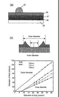
In order to make a solvent-formed via hole (figure 12(a)), a quantity of a
suitable
solvent 29 is deposited locally on top of the layers through which the via
hole is to
be formed. The solvent is selected so that it is capable of dissolving the
underlying layers through which the hole is to be formed. The solvent sinks
through the layers by progressive dissolution until the via hole is formed.
The
dissolved material is deposited onto the side walls W of the via-hole. The
type of
solvent and the method of depositing it may be selected for individual
applications. However, three preferred aspects are:
1. that the solvent and the process conditions are such that the solvent
evaporates or is otherwise readily removed so that it does not interfere with
subsequent processing and does not cause excessive or inaccurate
dissolution of the device; and
2. that the solvent is deposited by a selective process such as IJP, whereby
accurately controlled volumes of the solvent may be applied accurately to the
desired location on the substrate; and
3. that the diameter of the via hole is affected by the surface tension of the
solvent droplet and the ability of the solvent to wet the substrate; and
CA 02394895 2002-06-19
WO 01/47044
PCT/GB00/04940
28
4. that the solvent does not dissolve the underlying layer to which an
electrical
connection is to be made.
Figure 12(a) illustrates the deposition- of a droplet 29 of methanol solvent
(containing 20 ng per droplet) on a partially formed transistor device of the
general
type illustrated in figure 1(c). The partial device of figure 12(a) includes a
1.3 pm
thick PVP insulating layer 28, an F8T2 semiconducting layer 27, a PEDOT
electrode layer 26 and a glass substrate 25. In this example it is desired to
form a
via hole through the insulating PVP layer. Methanol is selected as the solvent
because of its ability to readily dissolve PVP; because it can easily
evaporate so
as not to hinder subsequent processing; and because it has satisfactory
wetting
properties for PVP. In order to form the via hole in this example an IJP
printing
head is moved to the location on the substrate at which the via hole is
desired to
be formed. Then the necessary number of suitably-sized droplets of methanol
are
dropped from the IJP head until the via is complete. The period between
successive drops is selected for compatibility with the rate at which the
methanol
dissolves the layers of the device. It is preferred that each drop has fully
or
almost fully evaporated before the next drop is deposited. Note that when the
via-
hole reaches the bottom non-polar semiconducting layer the etching stops such
that underlying layers are not removed. Other solvents such as isopropanol,
ethanol, butanol or actone may also be used. To achieve high throughput it is
desirable to complete the via-hole by deposition of a single solvent droplet.
For a
300 nm thick film and a droplet with a volume of 30 pl and diameter of 50 pm
this
requires the solubility of the layer in the solvent to be higher than 1-2 %
weight per
volume. A higher boiling point is also desirable if via-hole formation with a
single
droplet is required. In the case of PVP 1,2-dimenthy1-2-innidazolidinone (DMI)
with
a boiling point of 225 C can be used.
Figure 12(b) illustrates the effect of the dropping of several droplets of
methanol in
sequence onto the via hole location. The right panels show micrographs of the
CA 02394895 2002-06-19
WO 01/47044
PCT/GB00/04940
29
device after 1, 3 and 10 droplets have been dropped. The left panels show
Dektak surface profile measurements of the same devices across the via hole as
it is formed. (The location of the via hole is indicated generally at position
"V" in
each panel). When several droplets are deposited in sequence onto the same
location a crater opens up in the PVP film. The depth of the crater increases
as
successive droplets act, and after approximately 6 droplets the surface of the
underlying F8T2 layer is uncovered. The dissolved PVP material is deposited in
a
wall W at the sides of the via-hole. The diameter of the via-hole is on the
order 50
pm limited by the size of the droplet. This size is suitable for many
applications
such as logic circuits, and large area displays.
The via-hole diameter is determined by the size of the inkjet solvent
droplets. The
diameter of the hole was observed to be directly proportional to the diameter
of
the droplets (see Fig. 12c). The outer diameter of the side wall is determined
by
the size and spreading of the first droplet, and is independent of the
thickness of ,
the polymer layer that is dissolved. The inner diameter of the side wall
decreases
with increasing polymer thickness. For applications where even smaller holes
are
required, such as in high-resolution displays, even smaller droplet sizes can
be
used, or the substrate surface can be pre-patterned by a suitable technique to
confine the droplet on the surface as described above. Other solvents may
also=
be used.
It will be seen from the surface profile measurements that the formation of
the via
hole causes material to be dissolved and displaced to the edges of the via
hole,
where it remains after the solvent has been evaporated (indicated at W in
figure
12(b)). It should be noted that the displaced material is of a smoother
formation
than illustrated by figure 12(b) , the x and y axes of the surface profile
plots of
figure 12(b) being to dissimilar scales (x in units of pm, y in units of A).
CA 02394895 2002-06-19
WO 01/47044
PCT/GB00/04940
The mechanism for via-hole formation, i.e. the movement of material to the
side
walls, is believed to be similar to that of the well-known coffee-stain
effect, which
occurs if the contact line of a drying droplet containing a solute is pinned.
Pinning
can occur for example due to surface roughness or chemical heterogeneity. Note
that deposition of a good solvent always generates surface roughness during
dissolution. When the solvent evaporates, capillary flow occurs in order to
replace
the solvent evaporating near the contact line. More solvent is evaporating
near the
contact line because of the larger surface-to-bulk ratio near the contact
line. The
capillary flow velocity is large compared to the typical diffusion velocity,
such that
solute is carried to the edges of the droplet, and solute deposition occurs
only
near the rim, but not in the centre of the drying droplet (R.D. Deegan et al.,
Nature
389, 827 (1997)). Diffusion of solute would tend to favour homogeneous
redeposition of the polymer over the whole area upon drying of the solvent,
rather
than formation of a side wall. Theory predicts that the capillary flow
velocity v(r) (r:
distance from centre; R; droplet radius) is proportional to (R-r)4', where
9=(7c-
20c)/(27c-20c). Therefore, v increases with increasing X, that is decreasing
contact
angle O. Therefore, mass deposition at the edges occurs the faster the smaller
the contact angle.
For the opening of via-holes it is therefore important that (a) the contact
line of the
initial droplet is pinned, (b) that the contact angle of the droplets on top
of the
polymer to be dissolved is sufficiently small, and (c) that evaporation of the
solvent is sufficiently fast such that polymer solute diffusion can be
neglected. In
the case of IPA on PVP the contact angle is on the order of 12 , and the
droplets
typically dry within less than ls.
The smaller the contact angle, the faster will be the capillary flow velocity
inside
the droplet, i.e. the more reliable will be the formation of the side wall.
However,
on the other hand, the smaller the contact angle the larger the droplet
diameter.
An optimum contact angle therefore exists to achieve small diameter via-holes
with well-defined side walls. To achieve a larger contact angle for a good
solvent
CA 02394895 2002-06-19
WO 01/47044
PCT/GB00/04940
31
the surface of the substrate may be treated, for example with a self-assembled
monolayer with a larger repellence for the solvent. The self-assembled
monolayer
may be patterned, such as to provide hydrophobic and hydrophilic surface
regions, in order to confine the deposition of the solvent to a small area.
The depth and etch rate of the via hole can be controlled by a combination of
the
number of drops of solvent that are dropped, the frequency at which they are
deposited, and the rate of evaporation of the solvent in comparison to the
rate at
which it is capable of dissolving the substrate. The environment in which the
deposition takes place and the substrate temperature may influence the
evaporation rate. A layer of material that is insoluble or only slowly soluble
to the
solvent may be used to limit the depth of dissolution.
Since the layer sequence of the TFT consists of alternating polar and non-
polar
layers, it is possible to choose solvents and solvent combinations such that
etching stops at well defined depths.
In order to make contact through the via hole a conductive layer may be
deposited
over it so that it extends into the via hole and make electrical connection
with the
material at the bottom of the via hole. Figure 13(a) shows a device of the
type
shown in figure 12(a) but including a gold electrode 25 formed after the
making of
a via hole as described above.
Figure 13 shows at curve 30 the current voltage characteristics measured
between the bottom PEDOT electrode 25 and a conducting electrode 29
deposited on top of the PVP gate insulating layer 28. The diameter of the via
hole
was 50 pm. For comparison, curve 31 shows a reference sample, in which no via-
holes are located in the overlap region between the top and bottom electrodes.
The characteristics clearly show that the current through the via-hole is
several
orders of magnitude higher than the leakage current through the gate insulator
in
CA 02394895 2002-06-19
WO 01/47044
PCT/GB00/04940
32
the absence of the via hole. The measured current through the via hole is
limited
by the conductivity of the PEDOT electrodes, as can be seen by performing
conductivity measurements of the individual PEDOT electrodes. It is not
limited
by the resistance of the via-hole, such that only a lower limit estimate for
the via-
hole resistance R, can be obtained from these measurements: Rv < 500 ka
The method of via hole formation described above in relation to figure 12 is
directly applicable to depletion-type devices without a diffusion barrier (as
in figure
1(c)) and to devices in which the diffusion barrier is deposited after the
opening of
the via-holes. Figure 14(a) shows a device in which a via hole has been formed
and the gate electrode then deposited without an intervening diffusion barrier
layer. Figure 14(b) shows a similar device in which after formation of the via
hole
a diffusion barrier polymer 7 has been formed before deposition of the gate
electrode 6. In this case the diffusion barrier layer needs to exhibit good
charge
transporting properties in order to minimise the via-hole resistance R. A
suitable
diffusion barrier is a thin layer of TFB as shown in figure 5(a).
If an even lower contact resistance is required then the semiconductor layers
may
also be removed at the via hole site. This is preferably done after the
diffusion
barrier has been formed. The diffusion barrier 7 and the semiconducting
polymer
4 can be locally dissolved by IJP deposition of a good solvent for them - such
as
xylene in this example. By mixing good solvents for both the semiconducting
and
the insulating material, both layers may be dissolved at the same time. A
device in
which this has been done followed by deposition of the gate electrode is shown
in
figure 14(c).
Mixtures of solvents can also be used to reduce the diameter of the via-hole
by
increasing the contact angle of the solvent mixture on the layer to be
dissolved.
CA 02394895 2002-06-19
WO 01/47044
PCT/GB00/04940
33
An alternative technique to forming a via hole interconnection and then
depositing
a conductive material to bridge it is to locally deposit a material that is
capable of
locally modifying the underlying layer(s) substrate so as to render them
conductive. One example is the local IJP deposition of a solution containing a
mobile dopant that is able to diffuse into one or several of the layers. This
is
illustrated in figure 14(d), where region 32 indicates material that has been
rendered conductive by treatment with a dopant. The dopant may be a small
conjugated molecule such as a triarylamine like N,NP-diphenyl-N,N'-bis(3-
methylpheny1)-(1,11-biphenyl)-4,4'-diamine (TPD). The dopant is preferably
delivered as for the solvent case.
The method of via-hole formation through PVP dielectric layers can be used to
connect the gate electrode of the TFT to a source or drain electrode in the
underlying layer as required, for example, for a logic inverter device as
shown in
Fig. 15. Similar via-hole connections are required in most logic transistor
circuits.
Figure 16 shows plots of the characteristics of enhancement-load inverter
devices
formed with two normally-off transistor devices as in figure 15(b). Two
inverters
with different ratio of the channel width to channel length ratio (W/L) for
the two
transistors are shown (plot 35 ratio 3:1, plot 36 ratio 5:1)). It can be seen
that the
output voltage changes from a logic high (-20V) to a logic low (OV) state when
the input voltage changes from logic low to logic high. The gain of the
inverter,
that is the maximum slope of the characteristics is larger than 1, which is a
necessary condition to allow the fabrication of more complex circuits such as
ring
oscillators.
Via-holes as described above may also be used to provide electrical
connections
between interconnect lines in different layers. For complex electronic
circuits
multilevel interconnect schemes are required. This may be fabricated by
depositing a sequence of interconnects 72 and different dielectric layers 70,
71
deposited from compatible solvents (figure 15(d)). Via-holes 73 can then be
CA 02394895 2002-06-19
WO 01/47044
PCT/GB00/04940
34
formed in the way described above with the interconnect lines providing
automatic
etch stop.
Examples for suitable dielectric materials are polar polymers (70) such as PVP
and non-polar dielectric polymers (71) such as polystyrene. These can be
deposited alternatively from polar and non-polar solvents. Via-holes can be
opened by local deposition of good solvents for the respective dielectric
layer
while the underlying dielectric layer is providing an etch-stopping layer.
In selecting materials and deposition processes for devices of the type
described
above, it should be borne in mind that great advantages can be obtained if
each
layer is deposited from a solvent that does not substantially dissolve the
immediately underlying layer. In this way successive layers can be built up by
solution processing. One way to simplify selection of such materials and
process
steps is to aim to deposit two or more layers alternately from polar and non-
polar
solvents, as exemplified for the layer sequence described above. In this way
multilayer devices containing soluble, conducting, semiconducting and
insulating
layers can readily be formed. This can circumvent the problems of dissolution
and swelling of underlying layers.
The device structures, materials and processes described above are merely
illustrative. It will be appreciated that they may be varied.
Other device configurations than the top-gate configuration shown in figure 1
may
be used. An
alternative configuration is the more standard bottom-gate
configuration shown in figure 17, in which it is also possible to incorporate
a
diffusion barrier 7 and surface modification layer 8 if required. In figure 17
like
parts are numbered as for figure 1. Other device configurations with different
layer sequences may also be used. Devices other than transistors may be formed
in an analogous way.
CA 02394895 2002-06-19
WO 01/47044
PCT/GB00/04940
PEDOT/PSS may be replaced by any conducting polymer that can be deposited
from solution. Examples include polyaniline or polypyrrole. However, some of
the
attractive features of PEDOT/PSS are: (a) a polymeric dopant (PSS) with
inherently low diffusivity, (b) good thermal stability and stability in air,
and (c) a
work function of :=1 5.1 eV that is well matched to the ionisation potential
of
common hole-transporting semiconducting polymers allowing for efficient hole
charge carrier injection.
Efficient charge carrier injection is crucial in particular for short-channel
transistor
devices with channel lengths L < 10/./M. In such devices source-drain contact
resistance effects may limit the TFT current for small source-drain voltages
(figure
10(b)). In devices of comparable channel length it was found that injection
from
PEDOT source/drain electrodes is more efficient than injection from inorganic
gold
electrodes. This indicates that a polymeric source-drain electrode with an
ionisation potential that is well matched to that of the semiconductor may be
preferable to an inorganic electrode material.
The conductivity of PEDOT/PSS deposited from a water solution (Baytron P) is
on
the order of 0.1-1 S/cm. Higher conductivities up to 100 S/cm can be obtained
with formulations that contain a mixture of solvents (Bayer CPP 105T,
containing
isopropanol and N-methyl-2-pyrrolidone (NMP)). In the latter case care needs
to
be taken that the solvent combination of the formulation is compatible with
the
solubility requirements of the layer sequence. For applications in which even
higher conductivities are required other conducting polymers or solution-
processible inorganic conductors, such as colloidal suspensions of metallic
inorganic particles in a liquid, may be used.
The processes and devices described herein are not limited to devices
fabricated
with solution-processed polymers. Some of the conducting electrodes of the TFT
CA 02394895 2002-06-19
WO 01/47044 PCT/GB00/04940
36
=
and/or the interconnects in a circuit or display device (see below) may be
formed
from inorganic conductors, that can, for example, be deposited by printing of
a
colloidal suspension or by electroplating onto a pre-patterned substrate. In
devices in which not all layers are to be deposited from solution one or more
PEDOT/PSS portions of the device may be replaced with an insoluble conductive
material such as a vacuum-deposited conductor.
The semiconducting layer may also be replaced by another solution-processible
semiconducting material. Possibilities include small conjugated molecules with
solubilising side chains (J.G. Laquindanurri, et al., J. Am. Chem. Soc. 120,
664
(1998)), semiconducting organic-inorganic hybrid materials self-assembled from
solution (C.R. Kagan, et al., Science 286, 946 (1999)), or solution-deposited
inorganic semiconductors such as CdSe nanoparticles (B. A. Ridley, et al.,
Science 286, 746 (1999)).
The electrodes may be patterned by techniques other than ink-jet printing.
Suitable techniques include soft lithographic printing (J.A. Rogers et al.,
Appl.
Phys. Lett. 75, 1010 (1999); S. Brittain et al., Physics World May 1998, p.
31),
screen printing (Z. Bao, et al., Chem. Mat. 9, 12999 (1997)),
photolithographic
patterning (see WO 99/10939) or plating, or simple dip-coating of a patterned
substrate with hydrophobic and hydrophilic surface regions. Ink-jet printing
is
considered to be particularly suitable for large area patterning with good
registration, in particular for flexible plastic substrates.
Instead of a glass sheet, the device(s) could be deposited on to another
substrate
material, such as Perspex or a flexible, plastic substrate such as
polyethersulphone . Such a material is preferably in the form of a sheet, is
preferably of a polymer material, and may be transparent and/or flexible.
CA 02394895 2002-06-19
WO 01/47044
PCT/GB00/04940
37
Although preferably all layers and components of the device and circuit are
deposited and patterned by solution processing and printing techniques, one or
more components such as a semiconducting layer may also be deposited by
vacuum deposition techniques and/or patterned by a photolithographic process.
Devices such as TFTs fabricated as described above may be part of a more
complex circuit or device in which one or more such devices can be integrated
with each other and or with other devices. Examples of applications include
logic
circuits and active matrix circuitry for a display or a memory device, or a
user-
defined gate array circuit.
The basic component of a logic circuit is the inverter shown in figure 15. If
all
transistors on the substrate are either of the depletion or of the
accumulation type
three possible configurations are possible. The depletion-load inverter
(figure
15(a)) is suitable for device that are normally on, (figure 1(c) and 3), and
the
enhancement-load configuration (figure 15(b)) is used for normally-off
transistors
(figures 1(a/b) and 4). Both configurations require a via-hole between the
gate
electrode of the load transistor and its source and drain electrode,
respectively.
An alternative configuration is the resistance load inverter (figure 15(c)).
The
latter device can be fabricated by printing a thin, narrow PEDOT line of
adequate
length and conductivity as the load resistor. By reducing the conductivity of
PEDOT, for example by increasing the ratio of PSS to PEDOT, the length of the
resistor line can be minimized. The conductivity of Baytron P PEDOT/PSS with a
PEDOT/(PED0T+PSS) weight ratio of 0.4 was measured to be on the order of 0.2
S/cm for an as-deposited film. By annealing to 280 C for 20 min under N2
atmosphere the conductivity increased to 2 S/cm. By diluting the solution with
PSS the conductivity could be decreased by orders of magnitude. For a
PEDOT/(PED0T+PSS) weight ratio of 0.04 a conductivity of 10-3 S/cm was
measured after annealing at 280 C. Resistors with a resistance of 50 MO were
CA 02394895 2009-09-09
38
fabricated by inkjet printing a line of PEDOT with a width on the order of
600m and a length of 5000m.
The different inkjet printing components that have been developed, i.e.
transistors, via-hole interconnections, resistors, capacitors, multilayer
interconnect schemes etc., can be integrated to fabricate integrated
electronic
circuits by a combination of direct printing and solution processing. Inkjet
printing can be used for all processing steps where lateral patterning is
required. The simple inverter circuits described above are the building blocks
for more complex logic circuits.
Solution-processed TFTs as described above may be used as pixel switching
transistors of active matrix displays such as liquid-crystal (LCD) or
electrophoretic displays (B. Comiskey et al., Nature 394, 253 (1998)) for
which a suitable circuit is shown in figure 18(a); and light-emitting diode
displays (H. Sirringhaus, et al., Science 280, 1741 (1998), for which a
suitable
circuit is shown in figure 18(b); or as an active matrix addressing element of
a
memory device, such as a random access memory (RAM). In figures 18(a)
and (b) transistors T1 and/or T2 may be formed from transistors as described
above. Features 40 represent a display or memory element with current and
voltage supply pads.
In an example of a possible device configuration to control the voltage on the
electrode of a LCD or an electrophoretic displaythe gate insulating layer may
include a multilayer structure containing a diffusion barrier and/or surface
modification layer.
Referring to figure 18, the source and gate electrodes 2, 3 of the TFT are
connected to the data 44 and addressing 43 lines of the active matrix, which
may be fabricated from a different conducting material to achieve adequate
conductivity over longer lengths. The drain electrode 3 of the TFT may also be
the pixel electrode 41. The pixel electrode may be formed from a different
conducting material. In devices which rely on application of an electric field
rather than charge carrier injection it is not required that this electrode 41
is in
direct contact display element 40, such as a liquid crystal or electrophoretic
CA 02394895 2009-09-09
,
,
39
ink etc. In this configuration the total pixel area occupied by the TFT and
interconnect lines has to be kept small to achieve adequate aperture ratio and
to reduce potential cross-talk between the display element 40 and the signals
on the data and addressing lines 43 and 44.
According to another configuration the whole pixel or a large portion of the
pixel area is available for the TFTs and interconnect lines, and the display
element is shielded from the signals on the data and addressing lines 44, and
43 by the pixel electrode 41. Fabrication of this configuration requires an
additional dielectric layer 42 and a via-hole filled with conductive material
45
to connect the pixel electrode 41 to the TFT drain electrode 3. The via-hole
can be fabricated by the procedure described above.
Note that in this configuration the aperture ratio can be maximized and may
be approaching 100%. This configuration can also be used for display
application with a backlight such as transmissive LCD displays, since all-
polymer TFTs as fabricated here are highly transparent in the visible spectral
range. From optical absorption spectra measured on a F8T2 polymer TFT, in
which the polymer chains are aligned uniaxially by depositing the liquid-
crystalline semiconducting polymer on a rubbed polyimide alignment layer
which also serves as the pre-patteming layer for high-resolution printing, it
can be seen that the device is highly transparent in most of the visible
spectral
range because of the relatively high band gap of F8T2. Even better
transparency can be achieved if semiconducting layers such as F8 or TFB or
other polyfluorene derivatives (US 5,777,070) with higher band gaps are
used. The alignment of the polymer chains gives rise to optical anisotropy
such that light polarised parallel to the alignment direction (plot labelled
"I I") is
more strongly absorbed than light polarized perpendicular to the alignment
direction (plot labelled " I "). The optical anisotropy can be used in a LCD
display to further increase the optical transparency of the TFTs by orienting
the alignment direction of the polymer chains normal to the polarizer between
the glass backplane and the backlight. Under polarised light the transistor
devices appear almost colourless in visible light, if the thickness of the
F8T2
layer is below 500 A. All the other layers of the TFT including PEDOT has low
optical absorption in the visible spectral range.
CA 02394895 2009-09-09
Another advantage of the low optical absorption of the semiconducting layer is
the reduced photosensitivity of the TFT characteristics to visible light. In
the
case of amorphous silicon TFTs a black matrix has to be used to prevent
large OFF current under light illumination. In the case of polymer TFTs with
wide band gap semiconductors it is not required to protect the TFTs from
ambient light and from the backlight of the display.
A configuration well suited for the drive transistor T1 of an LED display
(figure
18(b)), allows the drive current of the TFT to be increased by fabrication of
an
interdigitated array of source-drain electrode with large channel width W
making use of the full area underneath the pixel electrode 41.
Alternatively, the bottom-gate TFT configuration of figure 17 can also be used
in all of the above applications.
One of the important technological issues for the fabrication of active matrix
circuits is the contact between the PEDOT/PSS TFT and pixel electrodes 2, 3,
6 and the metallic interconnect lines 43, 44, and 41. Due to its strong acidic
nature PEDOT/PSS is not compatible with many common inorganic metals
such as aluminium. Aluminium is easily oxidised in contact with PEDOT/PSS.
One possible solution is the fabrication of interconnect lines and pixel
electrodes 43, 44, and 41 from indium-tin-oxide (ITO) or tantalum, tungsten
and other refractory metals or another material having more stability in this
environment, or the use of a suitable barrier layer.
In the case of a display application it may also be desirable to fabricate
TFTs
with a small channel length by printing onto a pre-patterned substrate, as
described above.
Similar device configurations for active matrix transistor switches can also
be
used if the pixel element to be controlled is not a display element but a
memory element such as a capacitor or a diode, as for example in a dynamic
random access memory.
In addition to the conducting electrodes, some of the other layers of the TFTs
may also be patterned by direct printing methods, such as screen printing or
IJP. An active layer island of the semiconducting layer 4 and the gate
CA 02394895 2009-09-09
41
insulating layer 5 may be printed directly. In this case no via-holes are
required, but connections can be made by direct printing of a suitable gate
electrode pattern 6. In areas where addressing or interconnect lines 43, 44
overlap thick islands of a dielectric polymer 46 may be printed to provide
electrical insulation.
A plurality of devices formed as described above may be formed on a single
substrate and interconnected by conductive layers. The devices may be
formed on a single level or on more than one level, some devices being
formed on top of others. By use of interconnect strips and via-holes as
described above especially compact circuit arrangements may be formed.
The technology developed here for the fabrication of ink-jet printed
transistors,
via-holes and interconnect lines may be used to fabricate integrated
electronic
circuits by ink-jet printing. A prefabricated substrate containing an array of
hydrophilic and hydrophobic surface regions may be used that define the
channel length of the transistors and/or the width of the interconnect lines.
The substrate may also contain an array of highly conducting metallic
interconnect lines. Using a combination of ink-jet printing and deposition of
continuous layers from solution an array of transistor devices is defined in
custom locations and with custom channel widths. An integrated circuit is then
fabricated by forming electrical connections between pairs of transistors and
suitable interconnects using ink-jet printing of via- holes and conducting
lines.
It is also possible that the prefabricated substrate may already contain one
or
more of the components of the transistor devices. The substrate may contain,
for example, an array of completed inorganic transistor devices each having
at least one exposed electrode. In this case ink-jet fabrication of an
integrated
circuit would comprise the formation of electrical connections between pairs
of
transistors and the deposition of a single-or multilevel interconnect scheme
using ink-jet printed via-holes, interconnect lines, and isolation pads (see
figure 15(d)).
In addition to transistor devices the electronic circuit may also comprise
other
active and passive circuit elements such as display or memory elements or
capacitive or resistive elements.
CA 02394895 2009-09-09
42
Using the techniques described above a unit having a plurality of transistors
may be formed and then configured for a specific subsequent use by means
of solution-based processing. For example, a substrate having a plurality of
transistors of the type shown in figure 1(a), (b) or (c), in the form of a
gate
array, for example, may be formed on a plastic sheet. Other devices such as
diodes or capacitors may also be formed on the sheet. Then the sheet may be
placed in an ink-jet printer having a printing head for a suitable solvent for
forming via-holes (e. g. methanol) and a suitable material for forming
conductive tracks and for filling via-holes (e.g. PEDOT). The ink-jet printer
may be operable under the control of a suitable programmed computer,
having knowledge of the location and configuration of the transistors on the
sheet. Then, by a combination of via-hole formation and interconnection steps
the ink-jet printer can configure the circuit for performing a desired
electronic
or logic function, by interconnecting the transistors in the desired way. This
technology thus allows for the formation of logic-specific circuits on
substrates
using small, inexpensive apparatus.
Examples of the application of such a circuit are for printing of active
electronic tickets, luggage and identification tags. A ticket or tag printing
device may be loaded with a number of non-configured units each comprising
a substrate carrying a plurality of transistors. The ticket printing device
includes a computer that is capable of controlling an ink-jet printer as
described above and that is capable of determining an electronic circuit that
is
indicative of the valid function of the ticket. When required to print a
ticket the
printing device configures a substrate for the appropriate electronic circuit
by
printing via-holes and/or conductive material so that the transistors on the
substrate are appropriately configured. The substrate can then be
encapsulated, for example by sealing with adhesive plastics sheet, leaving
electrical connection terminals exposed. The ticket is then dispensed. When
the ticket is to be validated, inputs are applied to one or more input
terminals
and the outputs of the circuit at one or more output terminals are monitored
to
verify its functioning. The tickets could preferably be printed on flexible
plastic
substrates to make them convenient for use as tickets.
CA 02394895 2009-09-09
= =
43
User-defined circuits other than for pricing or tagging purposes may be
fabricated in a similar way. Verification and reading of the circuits may also
be
made by
CA 02394895 2002-06-19
WO 01/47044
PCT/GB00/04940
44
remote probing using for example radio frequency radiation (Physics World
March
1999, page 31).
The ability of the end-user to define circuits by simple ink-jet printing of
appropriate connections onto a standard array offers significantly increased
flexibility compared to factory-designed circuits.
The present invention is not limited to the foregoing examples. Aspects of the
present invention include all novel and/or inventive aspects of the concepts
described herein and all novel and/or inventive combinations of the features
described herein.
The applicant draws attention to the fact that the present inventions may
include
any feature or combination of features disclosed herein either implicitly or
explicitly or any generalisation thereof, without limitation to the scope of
any
definitions set out above. In view of the foregoing description it will be
evident to a
person skilled in the art that various modifications may be made within the
scope
of the inventions.