Note: Descriptions are shown in the official language in which they were submitted.
CA 02405149 2002-10-04
WO 01/74139 PCT/USO1/10951
HALL-EFFECT ELEMENT WITH INTEGRATED OFFSET CONTROL
AND METHOD FOR OPERATING HALL-EFFECT ELEMENT
TO REDUCE NULL OFFSET
s BACKGROUND OF THE INVENTION
The present invention is directed generally to a Hall-effect element
with offset control and a method for operating a Hall-effect element to reduce
null offset, and, in particular, a Hall-effect element with integrated offset
control and a method for operating a Hall-effect element having integrated
to offset control to reduce null offset.
Hall-effect elements are well known in the art. Hall-effect elements
rely on a reaction between a current flowing between a first set of contacts
and an orthogonally-applied magnetic field to generate a voltage across a
Is second set of contacts.
In theory, with no magnetic field applied to the Hall-effect element, no
voltage should be generated across the second set of contacts. In practice,
a voltage is typically generated across the second set of contacts even with
2o no magnetic field applied to the Hall-effect element. This voltage is
referred
to as null offset.
There are several reasons for the deviation between theory and
practice. For example, process variations in the fabrication of the Hall-
effect
2s element may cause local variations in resistance. Stress across the element
in either wafer or packaged form may also cause local variations in
resistance because of piezoresistive effects. Further, unbalance in the
subsequent amplifiers typically used with Hall-effecfi elements also can
contribute to null offset. .
While the null offset is usually quite small, it still can be large enough
to affect the proper operation of the Hall-effect element. As a consequence,
1
CA 02405149 2002-10-04
WO 01/74139 PCT/USO1/10951
a trimmer network is typically provided to balance the resistance variations.
For example, the trimmer network may include a current mirror with
trimmable degeneration resistors.
s Trimmer networks come with their own set of associated problems.
For example, Hall-effect elements are generally fabricated using a lightly
doped n-type layer for heightened sensitivity to variations in magnetic field
intensity. This means, however, that the element is also particularly
sensitive
to variations in temperature. As a consequence, the trimmer network must
to be able to adapt to the variations in resistance accompanying the
variations
in temperature. Furthermore, the subsequent amplifiers may also have
variations with temperature which require compensation.
One way to make the trimmer network responsive to variations in
is resistance accompanying the variations in temperature is to provide a large
reference resistor in close thermal proximity to the device that requires
temperature compensation. For example, the reference resistor may be
disposed in close proximity to the Hall-effect element, and coupled to the
associated trimmer network. In operation, the trimmer network directs a
2o portion of the current flowing through the reference resistor through the
one
of the Hall-effect element contacts to compensate for temperature-dependent
changes in resistance. If variations occur in subsequent amplifiers or
comparators, reference resistors must be provided for these devices as well.
2s Another way to achieve temperature compensation involves using
switches on the same chip as the Hall-effect element to direct current
alternatively to the separate sets of Hall-effect element contacts. The output
voltage difference between the two contacts is stored on a capacitor to allow
subsequent compensations of the Hall-effect element.
2
CA 02405149 2002-10-04
WO 01/74139 PCT/USO1/10951
Disadvantageously, these trimmer networks with their associated
compensation devices increase the size and complexity of the Hall-effect
elements, both in terms of fabrication and operation.
3
CA 02405149 2002-10-04
WO 01/74139 PCT/USO1/10951
SUMMARY OF THE INVENTION
The following summary of the invention is provided to facilitate an
understanding of some of the innovative features unique to the present
invention, and is not intended to be a full description. A full appreciation
of
s the various aspects of the invention can be gained by taking the entire
specification, claims, drawings, and abstract as a whole.
According to an aspect of the present invention, a Hall-effect element
includes an isolating layer and an active layer of a first electrical
conductivity
to type disposed on the isolating layer, the active layer having a surface. A
first
set of contacts is disposed in contact with the surface along a first axis,
and a
second set of contacts is disposed in contact with the surface along a second
axis transverse to the first axis. An insulating layer is disposed on the
surface, and a metal control field plate is disposed on the insulating layer.
A
Is voltage source is selectively coupleable to the metal control field plate
to
control~the accumulation of charge carriers at the surface of the active layer
to vary the resistance of the active layer.
According to another aspect of the present invention, a Hall-effect
2o apparatus includes a Hall-effect structure, a first set of contacts
disposed on
the structure along a first axis, and a second set of contacts disposed on the
structure along a second axis transverse to the first axis. A metal control
field plate is disposed in relation to the structure such that, when a voltage
is
selectively coupled to the metal control field plate, the Hall-effect
apparatus
Zs has a zero output in the absence of a magnetic field.
According to a further aspect of the present invention, a method is
provided for reducing null offset in a Hall-effect element. The method
includes the steps of providing an isolating layer, disposing an active layer
of
3o a first electrical conductivity type on the isolating layer, the active
layer
having a surface, disposing a first set of contacts on the surface along a
first
axis, disposing a second set of contacts on the surface along a second axis
4
CA 02405149 2002-10-04
WO 01/74139 PCT/USO1/10951
transverse to the first axis, and disposing an insulating layer on the active
layer. A voltage is applied across the insulating layer to control the
accumulation of charge carriers at the surface to vary the resistance of the
active layer.
The novel features of the present invention will become apparent to
those of skill in the art upon examination of the following detailed
description of
the invention or can be learned by practice of the present invention. It
should
be understood, however, that the detailed description of the invention and the
to specific examples presented, while indicating certain embodiments of the
present invention, are provided for illustration purposes only because various
changes and modifications within the scope of the invention will become
apparent to those of skill in the art from the detailed description of the
invention
and claims that follow.
5
CA 02405149 2002-10-04
WO 01/74139 PCT/USO1/10951
BRIEF DESCRIPTION OF THE DRAWINGS
The accompanying figures, in which like reference numerals refer to
identical or functionally-similar elements throughout the separate views and
which are incorporated in and form part of the specification, further
illustrate the
s present invention and, together with the detailed description of the
invention,
serve to explain the principles of the present invention.
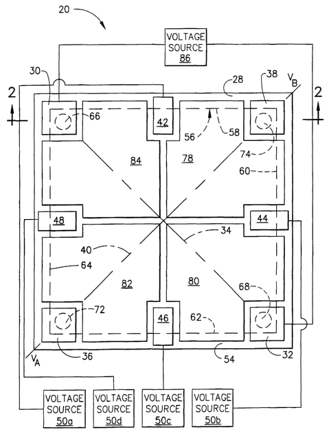
Fig. 1 is a schematic view of a Hall-effect element according to the
present invention;
to
Fig. 2 is a cross-sectional view taken along Line 2-2 in Fig. 1; and
Fig. 3. is a schematic view of a Wheatstone bridge equivalent circuit
for the Hall-effect element of Fig. 1.
6
CA 02405149 2002-10-04
WO 01/74139 PCT/USO1/10951
DETAILED DESCRIPTION OF THE INVENTION
An embodiment of a Hall-effect element 20 according to the present
invention is shown in Figs. 1 and 2. As shown in Fig. 2, the element 20
includes an isolating layer 22 and an active layer 24 of a first conductivity
s type disposed on the isolating layer 22. The layer 24 has a surface 26. An
insulating layer 28 is disposed on the layer 24 over a substantial portion of
the surface 26.
As shown in Fig. 1, a first set of contacts 30, 32 is disposed in contact
to with the surface 26 of the layer 24 along a first axis 34, and a second set
of
contacts 36, 38 is disposed in contact with the surface 26 of the layer 24
along a second axis 40 transverse to the first axis 34. Disposed on the layer
28 are four metal control field plates 42, 44, 46, 48 which are each
preferably
selectively and individually coupleable to a voltage source 50a, 50b, 50c,
Is 50d. The voltage sources 50a, 50b, 50c, 50d can have predetermined, fixed
voltages; alternatively, the voltage sources 50a, 50b, 50c, 50d can have
variable voltages, initially set to a predetermined voltage and varying
therefrom in accordance with changes in operating conditions.
2o In operation, voltage is applied to the control field plates 42, 44, 46, 48
to vary the accumulation of charge carriers at the surface 26 of the layer 24
(i.e., attract or repel the charge carriers). By changing the accumulation of
charge carriers at the surface 26, the resistance of the layer 24 can be
varied. That is, if more charge carriers are available in a given region, then
2s the resistance of the layer 24 in that region will decrease; conversely, if
fewer
charge carriers are available, then the resistance of the layer 24 will
increase.
By controlling the resistance of the layer 24, a substantially null at zero
applied magnetic field can be achieved.
3o Multiple control field plates 42, 44, 46, 48 are used in the embodiment
of the element 20 according to the present invention to allow for greater
selectivity in the control of the resistance of the layer 24. The number of
CA 02405149 2002-10-04
WO 01/74139 PCT/USO1/10951
control field plates can vary according to the degree to which control of
local
resistance is desired.
The method and apparatus by which voltage compensation is
s provided in element 20 has several advantages. The charge carriers
accumulated at the surface 26 of the layer 24 as a result of voltage applied
to
the control plates 42, 44, 46, 48 should have similar mobility as the charge
carriers in other regions of the layer 24, thereby providing inherent
temperature compensation. Further, the size and complexity of the
to compensation circuitry is reduced over that conventionally used.
The Hall-effect element 20 is now described in greater detail. The
isolating layer 22 is preferably a p-type silicon, and the active layer 24 is
preferably an n-type epitaxial silicon layer that is grown on the isolating
layer
is 22. Alternatively, the layer 22 can be silicon dioxide (Si02), and the
layer 24
may be a p-type silicon or any semiconductor material, such as gallium
arsenide. The active layer 24 has an active region 52 preferably bounded by
diffusion of p-type charge carriers into a boundary region 54 at an outer edge
56 of the active region 52. Alternatively, the boundary region 54 can be
2o silicon dioxide (Si02). The active region 52 has a square-shape with sides
58, 60, 62, 64, although other geometries (e.g., rectangular or truncated
square or rectangular) are possible. The insulating layer 28 (for example, a
p-type silicon or an insulator, such as silicon dioxide (Si02)) is grown over
the
active layer 24.
The first set of contacts 30, 32 is deposited over the insulating layer 28
along the first axis 34 in contact with heavily doped regions 66, 68 of the
layer 24 having the same type as the layer 24, thus defining a low-resistance
contact. Fig. 2 shows one of the ohmic contact regions 70 between the
3o contact 30 and the doped region 66. The second set of contacts 36, 38 are
deposited over the insulating layer 28 along the second axis 40 in contact
with doped regions 72, 74, defining ohmic contact regions, one of which is
s
CA 02405149 2002-10-04
WO 01/74139 PCT/USO1/10951
shown as 76. With the contacts of the first set of contacts 30, 32 and the
second set of contacts 36, 38 disposed at opposite corners of the square-
shaped active region 52, the first and second axes 34, 40 define the
diagonals of the square-shaped active region 52, and are thus substantially
s orthogonal to each other.
Four spaced metal (for example, aluminum) plates 78, 80, 82, 84 are
also deposited over the insulating layer 28. The metal plates 78, 80, 82, 84
substantially cover the active region 52 to shield the surface 26 from the
to effects of surface charge or electric fields. In the geometry shown in Fig.
1,
each of the shield plates 78, 80, 82, 84 covers a separate quadrant of the
square-shaped active region 52, and each is preferably connected to a
separate terminal, which can be coupled, for example to ground or V~~.
Alternatively, other arrangements and connections are possible; for example
is a single-shield plate can be used, or all of the plates can be connected to
a
single terminal.
Further, the control field plates 42, 44, 46, 48 are deposited on the
insulating layer 28, each plate along a different side 58, 60, 62, 64 of the
2o square-shaped active region 52. The control field plates 42, 44, 46, 48 are
spaced from each other and from the shield plates 78, 80, 82, 84. The
control field plates 42, 44, 46, 48 form MOS capacitor structures, and voltage
applied to the control field plates 42, 44, 46, 48 controls the accumulation
of
charge carriers on the surface 26 under the insulating layer 28. For typical
2s silicon device processing, positive surface state charges are formed at the
oxide-layer interface 26 (Fig. 2). Positive voltages applied to the control
field
plates 42, 44, 46, 48 increase the accumulation of n-type charge carriers at
the surface 26 and thereby decrease a local resistance in a corresponding
region of the layer 24 proximate to the control field plates 42, 44, 46, 48;
3o negative voltages decrease the accumulation charge carriers and thereby
increase resistance.
9
CA 02405149 2002-10-04
WO 01/74139 PCT/USO1/10951
In operation, the first set of contacts 30, 32 is coupled to a voltage
source 86, as shown. When a magnetic field is applied perpendicularly to the
Hall-effect element 20, the flow of charge carriers is skewed in the plane of
the layer 24 and is perpendicular to the flow of current between the first set
of
s contacts 30, 32. The resultant field produces an output voltage between the
second set of contacts 36, 38. The output voltage increases linearly with
voltage applied across the first set of contacts 30, 32 and the strength of
the
magnetic field, and is positive or negative depending on the polarity of the
magnetic field.
to
Without voltage applied to the control field plates 42, 44, 46, 48, the
voltage between the second set of contacts 36, 38 can include an offset
voltage component. The offset voltage, as discussed above, is caused by
local resistance variations due to fabrication flaws and material stresses,
for
is example. To balance the local resistances and limit the offset voltage,
voltage is applied to one or more of the control field plates 42, 44, 46, 48
to
vary the local resistances in the corresponding regions by varying the
accumulation of charge carriers at the surface 26. In fact, the shape and size
of the plates 42, 44, 46, 48 can be selected to assist in the control of the
local
2o resistances. In this manner, the offset voltage can be reduced to
substantially zero.
To further illustrate the Hall-effect element 20 according to the present
invention, an alternative representation for the Hall-effect element 20 is
2s shown in Fig. 3. In particular, a Wheatstone bridge equivalent circuit 88
for
the Hall-effect element 20 is shown. For an ideal Hall-effect element 20, in
which the local resistances R1, R2, R3, R4 are completely uniform and
dimensions are symmetrical, the output for zero magnetic field would be
zero. In a non-ideal Hall-effect element 20, where R1, R2, R3, R4 are not
3o initially uniform, the control field plates 42, 44, 46, 48 are used to vary
the
local resistances R1, R2, R3, R4 so that the output for zero magnetic field is
substantially zero (i.e., the bridge is balanced).
to
CA 02405149 2002-10-04
WO 01/74139 PCT/USO1/10951
The embodiments and examples set forth herein are presented to
best explain the present invention and its practical application and to
thereby enable those skilled in the art to make and utilize the invention.
s Those skilled in the art, however, will recognize that the foregoing
description and examples have been presented for the purpose of
illustration and example only. Other variations and modifications of the
present invention will be apparent to those of skill in the art, and it is the
intent of the appended claims that such variations and modifications be
to covered. The description as set forth is not intended to be exhaustive nor
to limit the scope of the invention. Many modifications and variations are
possible in light of the above teaching without departing from the spirit
and scope of the following claims. It is contemplated that the use of the
present invention can involve components having different characteristics.
is It is intended that the scope of the present invention be defined by the
claims appended hereto, giving full cognizance to equivalents in all
respects.
11