Note: Descriptions are shown in the official language in which they were submitted.
CA 02412416 2010-07-02
WO 02/09185 PCT/US01/23346
- 1 -
TITLE
Improved Window for GaN LED
TECHNICAL FIELD
This invention relates to GaN based Light Emitting Diodes (LED)
BACKGROUND OF THE INVENTION
A semiconductor light-emitting diode (LED) comprises: a substrate; a
light emitting region; a window structure and a pair of electrodes for
powering the
diode. The substrate may be opaque or transparent Light Emitting Diodes which
are based on Gallium Nitride compounds generally comprise: a transparent,
insulating substrate, e.g. a sapphire substrate. With a transparent substrate,
light
may be utilized from either the substrate or from the opposite end of the LED
which is termed the "window".
The amount of light generated by an LED is dependent on the distribution
of the energizing current across the face of the light emitting r'egion., It
is well
known that the current flowing between the electrodes tends to concentrate, in
a
favored path directly under the electrode. This tends to activate
corresponding
favored portions of the light emitting region to the exclusion of portions
which fall
outside the favored path. Further since such favored paths fall under the
opaque
electrode, the generated light reaching the electrode is lost. Prior art GaN
LEDs
have employed conductive current spreading layers formed of Ni/Au; and have
mounted a Au window bond pad on such layers. In such arrangements, the Ni/Au
layer and or the Au bond pad tend to peel during wire bonding to the pad.
DISCLOSURE OF THE INVENTION
In accordance with the present invention, light is utilized at the output of
the window structure which comprises: a very thin, semi-transparent Ni0õ1 Au
contact layer formed on a P doped Nitride compound window layer; a
semi-transparent amorphous conducting top window layer; and a P electrode
structure formed of a titanium layer with a covering Au bond pad. The
amorphous
CA 02412416 2011-05-16
WO 02/09185 PCT/US01/23346
- 2 -
top layer, by way .of example, may be formed of: Indium Tin Oxide (ITO); Tin
Oxide (TO) or Zinc Oxide (Zn0). Layers of other amorphous, conductive and
semi-transparent oxide compounds also may be suitable for construction of the
top
window layer.
Advantageously, the thin Ni0õ\ Au layer provides an excellent ohmic
connection to both the amorphous current spreading conducting layer and to the
Mg doped GaN window layer; the highly conductive amorphous layer efficiently
spreads current flowing between the electrodes across the light emitting
region to
improve the efficiency of the device.
Additionally, the titanium electrode passes through both the amorphous
conducting layer and the underlying Ni/Au to: (a) form an ohmic contact with
those layers; (b) contact the P doped top window layer and form a Shotticy
diode
connection therewith; and (c) provide good adhesion between Ti and the Mg
doped window layer. The Shottky diode connection forces current from the
electrode into the amorphous conducting layar and eliminates the tendency of
the
prior art structures to concentrate current in a path directly under the
electrode.
=
= BRIEF DESCRIPTION OF THE DRAWING
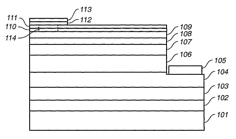
The Figure schematic showing of the side view of an illustrative
embodiment of our improved LED.
DETAILED DESCRIPTION
The illustrative LED of the Figure is a GaN based device in which light
exits through window 109.
The LED of the Figure includes a sapphire substrate 101, buffer region
102, GaN substitute substrate layer 103, N cladding layer 104, active region
106, P cladding layer 107, N electrode 105, and a window structure which
includes window layers 108,109, a thin NiOx\Au semi-transparent layer 110,
semi-transparent amorphous conducting layer 111, titanium electrode 112
and bond pad 113.
Layers 101 through 104, and layers 106 through 109 are grown in a Metal
CA 02412416 2010-07-02
WO 02/09185 PCT/US01/23346
- 3 -
Organic Chemical Vapor Deposition (MOCVD) reactor. The details of MOCVD
growth of the stated layers are well known in the industry and will not be
discussed herein.
The remaining components of the illustrative LED, namely, layers
NiOx\Au layer 110, amorphous conducting layer 111; N electrode 105, and P
electrode 112 and 113 are formed by evaporation in apparatus other than a
MOCVD reactor. Such processes are well known in the prior art and are not
described herein.
Light emitting structure
The illustrative light emitting structure of Fig. 1 comprises N cladding
layer 104, active region 106, and P cladding layer 107. Layer 104 is formed of
Silicon doped GaN.
In the illustrative example of Fig. 1, active region 106 is a Silicon doped
N type GaInN/GaN Multi Quantum Well (MQW) structure. Other forms of active
regions may be utilized with our improved window structure.
P cladding layer 107 is formed of Mg doped AlGaN.
Window layers
The first window layer 108 is formed of Mg doped GaN. Layer 108 has a
nominal thickness of 300nm. The second window layer 109 is similarly formed of
Mg doped GaN. However, layer 109 is more highly doped to permit an ohmic
contact between that layer and the very thin Ni0õ\Au layer 110.
Completion of the MOCVD growth process
Growth of P type GaN layers is achieved with introduction of gaseous
flows of TMG with H2 as a carrier gas, NH3 as a group V material, and Mg as a
dopant. In the absence of an appropriate cool down protocol, Hydrogen
passivation of the Mg may occur. In which case, the conductivity of a Mg doped
layer is reduced.
In order to avoid Hydrogen passivation of the Mg doped layers 107, 108
and 109, the following described cool down protocol has been adopted upon
completion of the MOCVD growth.
CA 02412416 2010-07-02
-.4-
1. The ambient gas of the reactor is switched from 112 to nitrogen N2
immediately after completion of the LED structure;
2. The reactor temperature is ramped down from the growth temperature
to about 900 degrees C in about 2 minutes;
3. The flow of NH3 is terminated;
4. The reactor temperature is further ramped down to about 750 degrees
C. in about 2 minutes;
5. Temperature of about 750 degrees C is held for about 20 minutes;
6. The heater of the reactor is shut off and the reactor is allowed to
complete cool-down naturally. Experience shows that cool-down to
120 degrees C occurs in about 30 minutes after heater shut off.
The resulting product exhibits the expected desired physical and electrical
characteristics.
Formation of the Electrode Structures
Fig. 1 illustrates the locations of both p electrode layers 111, 112 and N
electrode 105.
Layer 110 is a very thin, semi-transparent contact layer of NiOx /Au which is
deposited over the entire exposed face of window layer 109. Opening 114 is
formed
in layers 110 and 111 to permit the deposit of a titanium adhesion layer 112
to contact
window layer 109. Titanium forms a strong physical bond with layer 109 and
thus
tends to eliminate peeling during wire bonding. In addition to reaching
through to
layer 109, titanium layer 112 is a structure that is deposited through and on
top of
=
amorphous layer 111. Titanium layer 112 serves as a titanium electrode that
forms
ohmic contacts with layers 110 and 111, and forms a Schottky diode contact
with
window layer 109. The Schottky diode connection to window layer 109 eliminates
the current path directly under the electrode and forces current flowing
between the
electrodes into conducting layer 111.
P electrode Au bond pad 113 is deposited on top of titanium layer 112 to form
an ohmic contact.
Since the Mg doped layers do not suffer from Hydrogen passivation, it is not
necessary to heat treat the structure to activate the Mg doping in those
layers.
However, Ni/Au layer 110 and the Ti and Au contact structures are heated in an
CA 02412416 2010-07-02
WO 02/09185 PCT/US01/23346
- 5 -
atmosphere of molecular nitrogen and air. Thus, the Ni is converted to a form
of
nickel oxide. The described heat treatment improves the quality of the contact
structures.
The invention has been described with particular attention to its preferred
embodiment; however, it should be understood that variations and modifications
within the spirit and scope of the invention may occur to those skilled in the
art to
which the invention pertains.
=