Note: Descriptions are shown in the official language in which they were submitted.
CA 02412421 2002-12-20
WO 02/09200 PCT/USO1/23359
-1
TITLE
Enhanced Light-emitting diode
TECHNICAL FIELD
This invention relates to light-emitting diodes formed of AIGaInP
compounds.
BACKGROUND OF THE INVENTION
A semiconductor light-emitting diode comprises: a substrate; a light
emitting structure; and a pair of electrical contacts for powering the diode,
i.e., a
substrate contact and a window contact. The substrate may be transparent or
opaque; and the "substrate" contact, is formed on a surface thereof. The
window
contact is formed on a window surface.
LED structures composed of AIGaInP compounds can be designed to emit
any selected one of a range of colors by tailoring the amount of A1 in the
compound. However, where the substrate and lower cladding layer are of n type
AIGaInP compounds, it is difficult to achieve a low resistance p type AIGaInP
compound for the upper cladding layer. Unfortunately, a relatively high
resistance
upper cladding layer does not provide full use of the surface of the light
emitting
structure. That is, current flowing between the window and substrate
°:contacts
tends to concentrate in a narrow "favored" path, which lies directly under the
window contact. Thus, only that portion of the light emitting surface which
lies in
the favored path is activated.
A number of prior art arrangements provide a "window" which is
interposed between the light emitting structure and the window contact to more
fully utilize the light emitting surface. The prior art windows range from a
single
thick layer of compounds other than AIGaInP to a variety of mufti layer
structures
which "spread" the energizing current across the face of the light emitting
surfaces.
Light generated by an LED exits directly from the outer face of the light
emitting surface or via the window. The "window" contact is formed on the
outer
SUBSTITUTE SHEET (RULE 26)
CA 02412421 2002-12-20
WO 02/09200 PCT/USO1/23359
-2-
blocl~s emission of light generated directly thereunder. For example, in the
case of
an LED having a 10 mil by 10 mil square window, a four mil round metal contact
will obscure about 12.2 % of the window surface. However, the window contact
cannot be measurably reduced in diameter, since the contact must be large
enough
to insure its adhesion to the wiildow surface.
DISCLOSURE OF THE INVENTION
Our semiconductor light-emitting diodes comprise: a substrate; a substrate
electrical contact; a light emitting structure; and an improved window. Our
window interfaces directly with the light emitting structure; and, in the
following
stated order comprises: a lightly doped p GaP layer; a low resistance p GaAs
layer; a transparent, amorphous conducting window layer, and a metal window
contact. The conducting layer, by way of example, may be formed of: Indium Tin
Oxide (ITO); Tin Oxide (TO) or Zinc Oxide (Zn0). Layers of other amorphous,
conductive and transparent oxide compounds also may be suitable for
construction
of the window layer.
In a first embodiment of our invention, the metal contact passes through
both the conducting layer and the GaAs layer to: (a) form an ohmic contact
with
those layers and (b) contact the GaP layer and form a Shottlcy diode
connection
therewith.
In a second embodiment of our invention, the metal contact passes only
through the conducting layer and it contacts an insulator which is formed in
the
GaAs layer to isolate the metal contact from the GaP layer. As in our first
embodiment, the metal window contact forms an ohmic contact with the
conducting layer and the GaAs layer.
Advantageously, in both embodiments, the current path lying directly
under the metal contact is eliminated and the current is widely spread over
the face
of the light emitting structure.
With elimination of the "favored" path, less light is generated from the
portion of the diode interface which is directly under the window contact; and
more light is generated from the remaining surface of that interface. The net
result
being an increase in the total light emitted through the window layer.
CA 02412421 2002-12-20
WO 02/09200 PCT/USO1/23359
-3-
Advantageously, in accordance with this invention, all of the diode, other
than: the metal contacts, and the conducting layer, is grown in a continuous
process.
BRIEF DESCRIPTION OF THE DRAWING
FIGS. 1A and 1B are top and side views of a prior art LED;
FIGS. 2A and 2B are top and side views of a first embodiment of an LED
in accordance with the present invention;
Fig. 3 is a side view of a second embodiment of an LED in accordance
with the present invention;
DETAILED DESCRIPTION
The top view representations of Figs. 1A and 2A are drawn to scale;
however the side view representations of Figs. 1B and 2B are not to scale. The
top
view of Figure 1A represents an LED having a 10 mil by 10 mil square window
105 with a 4 mil circular metal contact 145. Typically, the window contact is
gold. The prior art LED of Fig. 1B comprises a metal substrate contact 101, an
"n" GaAs substrate 102, an "n" cladding layer 103; an active region 104; a
p cladding layer 105; and a metal window contact 106. As explained earlier
herein, current which flows between the window contact 106 and the substrate
contact 101 concentrates in a "favored" path directly under the window
contact 101. Since, only a small area of the active layer lies in that current
path,
much of the light emitting potential of the LED is dormant. Additionally, most
of
the light emitted through layer 105 is intercepted by the opaque contact 106.
It has
been observed that, under the stated conditions, the light which is emitted by
the
LED appears as a thin halo surrounding contact 106.
A first embodiment of our improved LED is illustrated schematically in
Figs. 2A and 2B. The top view of Figure 2A represents an LED having a 10 mil
by 10 mil square amorphous transparent layer 209 surrounding a 5 mil circular
metal contact 210.
In Fig. 2B, elements 201 through 206 form a light emitting diode; and the
first embodiment of our improved window comprises elements 207 through 210.
In the example of Fig. 2B, the elements 203 through 208 are grown in
CA 02412421 2002-12-20
WO 02/09200 PCT/USO1/23359
-4-
sequence upon substrate 202 which is a single crystal n doped GaAs wafer.
Element 203 is an optional Distributed Bragg Reflector (DBR); layer 204 is an
n
AIGaInP lower cladding layer; element 205 is an active region; layer 206 is a
p
AIGaInP upper cladding layer; 207 is a lightly doped p GaP first window layer;
208 is a low resistance p GaAs second window layer; 209 is an amorphous,
transparent conducting layer; and 210 is a metal window contact.
In this first embodiment of our invention, layers 207 through 209, and
contact 210 form our improved window.
First window layer 207 is formed of p doped GaP. Second window
layer 208 is formed of p doped GaAs. Layer 209 is formed of an amorphous
conducting material having a thiclaless of 100 to 1,000 mn; and window contact
210 is formed of gold or of a gold compound. The conducting layer may be
formed of Indium Tin Oxide (ITO); Tin Oxide (TO) or Zinc Oxide (Zn0).
Contact 210 may be formed of Ti\Au.
Layers 203 through 208 are grown in a continuous MOCVD process.
After such growth is completed, hydrogen Garner gas flow is terminated, and
flowing molecular nitrogen gas is introduced into the reactor. The reactor
temperature is then reduced to a value below the growth temperature and the
flow
of the growth gases is stopped. The remaining cool down of the reactor to room
temperature includes a period of annealing of the GaAs layer 208 at a
temperature
of about 600 degrees C. This avoids passivation of the p dopant in layer 208.
The completed wafer, as forned above, is removed from the MOCVD
reactor and completion of the remainder of the LED of Fig. 2b is implemented
as
follows. The amorphous conducting layer, e.g. ITO, is installed by sputtering
on
top of the second layer 208. A hole is etched through layers 209 and 208 to
reach
layer 207. A titanium\gold compound is then evaporated into the resulting void
and over layer 209 as illustrated in Fig. 2B. In this first embodiment, the
interface
between contact 210 and the lightly doper GaP layer 207 forms a Shottlcy
diode.
Thus, with the low operating voltage applied to contacts 201 and 210, the
Shottl~y
diode inhibits flow of energizing current directly from contact 210 to layer
207.
Our enhanced window structure of Fig. 2B, eliminates the favored cunent
CA 02412421 2002-12-20
WO 02/09200 PCT/USO1/23359
-5-
path through the LED directly under the window contact 210; and widely
distributes the energizing current quite evenly over a substantial portion of
the face
of the active layer. Accordingly, the light emitted through the window is
increased without increasing either the surface area of the active layer; or
the
energizing current requirements.
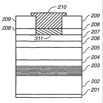
Fig. 3 illustrates schematically the second embodiment of our improved
window. Those elements of Fig. 3 which are unchanged from Fig. 2B retain the
numbers of Fig. 2. Our window of Fig. 3 further includes insulator 311 which
is
formed in layer 208 after a hole has been etched in the amorphous layer 209
and in
the GaAs layer 208. Insulator 211 is formed by evaporation of Silicon Oxide.
The thickness of the insulator may be equal to, or slightly greater than, the
thickness of layer 208. As in the production of our window of Figs. 2a and 2b,
a
titanium\gold metal contact 210 is evaporated in the unfilled portion hole and
on
top of amorphous layer 209. In this second embodiment, the metal window
contact 210 forms an ohmic connection with amorphous layer 209 and is
insulated
from the first layer 207. This second embodiment serves to eliminate the
favorite
current path under the window contact 210 and widely spreads the energizing
current across the surface of active layer 205.
Our window structures can be used with any LED composed of AIGaInP
compounds without limitation of the form of the light emitting structure; and
with
or without the optional Distributed Bragg Reflector.
The invention has been described with particular attention to its preferred
embodiment; however, it should be understood that variations and modifications
within the spirit and scope of the invention may occur to those skilled in the
art to
which the invention pertains.