Language selection

Search

Patent 2414725 Summary

Third-party information liability

Some of the information on this Web page has been provided by external sources. The Government of Canada is not responsible for the accuracy, reliability or currency of the information supplied by external sources. Users wishing to rely upon this information should consult directly with the source of the information. Content provided by external sources is not subject to official languages, privacy and accessibility requirements.

Claims and Abstract availability

Any discrepancies in the text and image of the Claims and Abstract are due to differing posting times. Text of the Claims and Abstract are posted:

  • At the time the application is open to public inspection;
  • At the time of issue of the patent (grant).
(12) Patent: (11) CA 2414725
(54) English Title: IMPROVED GAN LIGHT EMITTING DIODE
(54) French Title: DIODE GAN D'EMISSION LUMINEUSE AMELIOREE
Status: Expired
Bibliographic Data
(51) International Patent Classification (IPC):
  • H01L 33/32 (2010.01)
(72) Inventors :
  • CHEN, JOHN (United States of America)
  • LIANG, BINGWEN (United States of America)
  • SHIH, ROBERT (United States of America)
(73) Owners :
  • DALIAN MEIMING EPITAXY TECHNOLOGY CO., LTD. (China)
(71) Applicants :
  • AMERICAN XTAL TECHNOLOGY, INC. (United States of America)
(74) Agent: GOWLING WLG (CANADA) LLP
(74) Associate agent:
(45) Issued: 2012-01-03
(86) PCT Filing Date: 2001-07-25
(87) Open to Public Inspection: 2002-01-31
Examination requested: 2006-07-18
Availability of licence: N/A
(25) Language of filing: English

Patent Cooperation Treaty (PCT): Yes
(86) PCT Filing Number: PCT/US2001/023452
(87) International Publication Number: WO2002/009475
(85) National Entry: 2002-12-24

(30) Application Priority Data:
Application No. Country/Territory Date
09/626,443 United States of America 2000-07-26

Abstracts

English Abstract


A GaN based LED comprises: a three layer buffer (11) which is a template for
growth of a high quality I GaN platform for quality growth of subsequent
layers; a light emitting structure (12); and complementary N and P electrode
structures (115, 113) which spread current flowing between the electrodes
fully across the light emitting structure (12).


French Abstract

La présente invention concerne une DEL à base de GaN comprenant: un tampon à trois couches qui est un élément de référence pour la croissance d'une plate-forme haute qualité I GaN permettant une bonne croissance des couches suivantes; une structure d'émission lumineuse; et des structures d'électrode complémentaires N et P qui produisent un courant circulant entre les électrodes en traversant complètement la structure d'émission lumineuse.

Claims

Note: Claims are shown in the official language in which they were submitted.


6
CLAIMS:

1. A GaN based Light Emitting Diode comprising:
a substrate;
a light emitting structure comprising an N cladding layer, an active region,
and a
P cladding layer;

a window structure grown on said P cladding layer;
an N electrode in ohmic contact with said N cladding layer; and
a P electrode in ohmic contact with said P cladding layer, wherein:
said window structure comprises a thin, transparent, conductive outer layer
having
an exposed surface with four sides; and
a complementary pair of P and N electrodes formed along opposite sides of said

exposed surface, wherein:

said P electrode is formed on said exposed surface and has a T-shape when
viewed from the top, with a head of the T-shape being a bar formed along one
side of
said exposed surface, and a leg of the T-shape being a semi circular portion
which joins
the bar; and

said N electrode comprises a bond pad assembly formed on said N cladding layer

through an aperture located at the middle of the side of the face opposite to
said one side.
2. A GaN based Light Emitting Diode in accordance with claim 1 wherein:
said conductive outer layer is a NiOx/Au layer.

3. A GaN based Light Emitting diode in accordance with claim 2 wherein:
said P electrode comprises a layer of Ti formed on said conductive layer and a

layer of Au in the same shape formed on said Ti layer.

Description

Note: Descriptions are shown in the official language in which they were submitted.


CA 02414725 2002-12-24
WO 02/09475 PCT/USO1/23452
-1_
TITLE
Improved GaN Light Emitting Diode
TECHNICAL FIELD
This invention relates to GaN compound Light Emitting Diodes.
BACKGROUND OF THE INVENTION
A semiconductor light-emitting diode (LED) comprises: a substrate; a light
emitting structure; and a pair of electrodes for powering the diode. Light
Emitting
Diodes which are based on Gallium Nitride compounds generally comprise: a
transparent, insulating substrate, e.g. a sapphire substrate. With an
insulating
substrate, both electrodes must be connected from the front of the LED to
layers of
the light emitting structure.
It is common practice to utilize a Ni/Au contact layer between the window
layers formed on the light emitting structure and a thick Au bond pad. This
arrangement exhibits limited adhesion; and the contact layer tends to peel
during
wire bonding to the Au bond pad.
The magnitude of the light emitted by an LED depends on: (a) The percent
of the light emitting region that is activated by current flowing between the
electrodes; (b) The efficiency of the window structure; and (c) The internal
losses
of generated light.
DISCLOSURE OF THE INVENTION
In accordance with one aspect of our present invention, we provide a
window structure which comprises: a semi-transparent, conductive outer layer
and
a complementary pair of P and N electrodes. The conductive outer layer and the
electrodes together efficiently spread current across the face of the light
emitting
diode and maximize the light emitting area of the window. Our P electrode is
formed in the shape of a stylized letter T. The head of the T is a bar formed
on the
top face of the window along one side of the window face. The leg of the T
comprises a bond pad attached at the middle of the head. Our N electrode


CA 02414725 2002-12-24
WO 02/09475 PCT/USO1/23452
_2_
comprises a bond pad assembly which attaches to the N cladding layer through
an
aperture located at the middle of the side of the face opposite to the head of
the T.
Our P electrode is formed of a layer of Ti which passes through the contact
layer and provides excellent adhesion to window layers formed on the light
emitting structure. An Au bond pad is formed on, and in the form of the Ti
electrode. Thus peeling is avoided.
BRIEF DESCRIPTION OF THE DRAWING
Figs. la and 1b are schematic showings of the top and side views of an
illustrative embodiment of our improved LED.
DETAILED DESCRIPTION
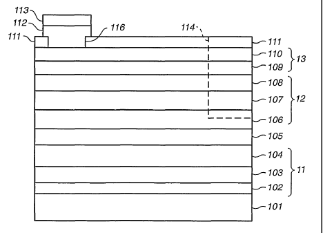
The illustrative LED of Figs. la and 1b is a GaN based device. The
structure of Figs. 1a and 1b comprises: sapphire substrate 101; buffer
structure 11;
GaN substitute substrate layer 105; light emitting structure 12; window layers
13;
semi transparent conductive layer 111; bond pad adhesion layer 112; P
electrode
bond pad 113; and N electrode bond pad 115 which is not shown in Fig. 1b.
Layers 102 through 110 are grown in a Metal Organic Chemical Vapor
Deposition MOCVD reactor. The details of MOCVD growth of the stated layers
are well known in the industry and will not be discussed herein except to
specify
certain details of the growth process which are particularly relevant to our
success.
The remaining components of our improved LED, namely, semi
transparent layer 111, adhesion pad 112, P bond pad 113, and N bond pad 115
are
formed by evaporation in apparatus other than a MOCVD reactor.
Buffer ~ 1 ) between sapphire substrate and GaN
In the illustrative embodiment of our improved GaN based LED, the 0001
face of sapphire substrate 101 is exposed for growth of our first buffer layer
102.
Our second buffer Layer 103 is formed of Al GaN to migrate to the lattice
constant
of GaN. The final buffer layer 104 is formed of GaN to provide a template for
the
growth of our high quality I GaN layer 105 which serves as a platform for
growth
of our light emitting structure 12.


CA 02414725 2002-12-24
WO 02/09475 PCT/USO1/23452
-3-
L_ fight emitting structure~l2)
Our light emitting structure comprises N cladding layer 106, active region
107, and P cladding layer 108. Layer 106 is formed of Silicon doped GaAs.
In the illustrative example of Fig. 1b, active region 107 is a Silicon doped
N type GaInN/GaN Multi Quantum Well (MQW) structure.
P cladding layer 108 is formed of Mg doped AIGaN.
Window layers
The first window layer 109 is foamed of Mg doped GaN. Layer 109 has a
nominal thickness of 300 nm. The second window layer 110 is similarly formed
of Mg doped GaN. However, layer 110 is more highly doped to permit an ohmic
contact between that layer and NiOX/Au contact layer 111.
Completion of the MOCVD . rowth rp ocess
Growth of GaN layers is achieved with introduction of gaseous flows of
Gallium with H2 as a carrier gas, NH3 as a group V material, and Mg as a
dopant.
In the absence of an appropriate cool down protocol, Hydrogen passivation of
the
Mg may occur. In which case, the conductivity of a Mg doped layer is reduced.
In order to avoid Hydrogen passivation of the Mg doped layers 108, 109
and 110, the following described cool down protocol has been adopted upon
completion of the MOCVD growth.
1. The ambient gas of the reactor is switched from H2 to N2
immediately after completion of the LED structure;
2. The reactor temperature is ramped down from the growth
temperature to about 900 degrees C in about 2 minutes;
3. The flow of NH3 is terminated;
4. The reactor temperature is further ramped down to about 750
degrees C in about 2 minutes;
5. Temperature of about 750 degrees C is held for about 20 minutes;
6. The heater of the reactor is shut off and the reactor is allowed to
complete cool down naturally. Experience shows that cool down to 120 C occurs
in about 30 minutes after heater shut off.
The resulting product exhibits the expected desired physical and electrical


CA 02414725 2002-12-24
WO 02/09475 PCT/USO1/23452
-4-
characteristics.
Formation of the electrode structures
The top view of Fig. la and the side view of Fig. 1b together illustrate the
locations and forms of both the P electrode 113 and of the N electrode 11 S.
S Layer 111 is a thin, semi-transparent, conductive layer of NiOx/Au which
is deposited over the entire exposed face of layer 110. A first opening,
identified
as I 14 in both figures, is etched through layers 111 to 107 to reach N
cladding
layer 106.
As seen in Fig. 1 a, a second opening 1 I 6 is formed in layer 1 I 1 to permit
deposit of a Titanium adhesion structure 112 to contact window layer 110. In
addition to reaching through to layer 110, titanium structure 112 is deposited
on
NiOX/Au layer 111 in the shape of the Au bond pad as illustrated in Fig. 1 a.
As
seen in Fig. 1 a, the top view of the Au bond pad forms a stylized "T". The
bar of
the T is deposited as shown along left side of the figure, and the leg of the
T is the
1S semi-circular portion which joins that bar. The Au bond pad 113 is
deposited on
top of titanium structure 112.
Gold Bond pad 11 S is deposited on N cladding layer 106 to form an ohmic
contact therewith.
The combination of the T bar of the P electrode bond pad 113 along one
side of the outer surface, the conductive NiOX/Au layer 11 l, and the
placement of
the N electrode centrally along the opposite side of the outer face spreads
current
flowing between the electrodes evenly to more fully activate the light
emitting
region of MQW structure 107.
Since the Mg doped layers do not suffer from Hydrogen passivation, it is
2S not necessary to heat treat the structure to activate the Mg doping in
those layers.
However, we do heat NiOX/Au layer 111 and the Ti and Au contact structures in
an atmosphere of molecular nitrogen and air. Thus the Ni is converted to a
form
of niclcel oxide. We have found that this heat treatment improves the quality
of
the contact structures.
The invention has been described with particular attention to its preferred
embodiment; however, it should be understood that variations and modifications


CA 02414725 2002-12-24
WO 02/09475 PCT/USO1/23452
-5-
within the spirit and scope of the invention may occur to those skilled in the
art to
which the invention pertains.

Representative Drawing
A single figure which represents the drawing illustrating the invention.
Administrative Status

For a clearer understanding of the status of the application/patent presented on this page, the site Disclaimer , as well as the definitions for Patent , Administrative Status , Maintenance Fee  and Payment History  should be consulted.

Administrative Status

Title Date
Forecasted Issue Date 2012-01-03
(86) PCT Filing Date 2001-07-25
(87) PCT Publication Date 2002-01-31
(85) National Entry 2002-12-24
Examination Requested 2006-07-18
(45) Issued 2012-01-03
Expired 2021-07-26

Abandonment History

There is no abandonment history.

Payment History

Fee Type Anniversary Year Due Date Amount Paid Paid Date
Application Fee $300.00 2002-12-24
Maintenance Fee - Application - New Act 2 2003-07-25 $100.00 2002-12-24
Registration of a document - section 124 $100.00 2003-11-28
Registration of a document - section 124 $100.00 2004-06-18
Maintenance Fee - Application - New Act 3 2004-07-26 $100.00 2004-07-02
Maintenance Fee - Application - New Act 4 2005-07-25 $100.00 2005-06-28
Request for Examination $800.00 2006-07-18
Maintenance Fee - Application - New Act 5 2006-07-25 $200.00 2006-07-19
Maintenance Fee - Application - New Act 6 2007-07-25 $200.00 2007-07-04
Maintenance Fee - Application - New Act 7 2008-07-25 $200.00 2008-07-07
Maintenance Fee - Application - New Act 8 2009-07-27 $200.00 2009-05-28
Maintenance Fee - Application - New Act 9 2010-07-26 $200.00 2010-07-08
Registration of a document - section 124 $100.00 2011-06-01
Maintenance Fee - Application - New Act 10 2011-07-25 $250.00 2011-07-13
Final Fee $300.00 2011-10-17
Maintenance Fee - Patent - New Act 11 2012-07-25 $450.00 2012-10-30
Maintenance Fee - Patent - New Act 12 2013-07-25 $250.00 2013-06-25
Maintenance Fee - Patent - New Act 13 2014-07-25 $250.00 2014-07-24
Maintenance Fee - Patent - New Act 14 2015-07-27 $250.00 2015-07-22
Maintenance Fee - Patent - New Act 15 2016-07-25 $450.00 2016-07-21
Maintenance Fee - Patent - New Act 16 2017-07-25 $450.00 2017-07-21
Maintenance Fee - Patent - New Act 17 2018-07-25 $450.00 2018-07-18
Maintenance Fee - Patent - New Act 18 2019-07-25 $450.00 2019-07-17
Owners on Record

Note: Records showing the ownership history in alphabetical order.

Current Owners on Record
DALIAN MEIMING EPITAXY TECHNOLOGY CO., LTD.
Past Owners on Record
AMERICAN XTAL TECHNOLOGY, INC.
AXT, INC.
CHEN, JOHN
DALIAN LUMING SCIENCE AND TECHNOLOGY GROUP CO., LTD.
LIANG, BINGWEN
SHIH, ROBERT
Past Owners that do not appear in the "Owners on Record" listing will appear in other documentation within the application.
Documents

To view selected files, please enter reCAPTCHA code :


To view images, click a link in the Document Description column. To download the documents, select one or more checkboxes in the first column and then click the "Download Selected in PDF format (Zip Archive)" or the "Download Selected as Single PDF" button.

List of published and non-published patent-specific documents on the CPD .

If you have any difficulty accessing content, you can call the Client Service Centre at 1-866-997-1936 or send them an e-mail at CIPO Client Service Centre.


Document
Description 
Date
(yyyy-mm-dd) 
Number of pages   Size of Image (KB) 
Abstract 2002-12-24 2 60
Claims 2002-12-24 1 36
Drawings 2002-12-24 1 11
Description 2002-12-24 5 203
Representative Drawing 2002-12-24 1 6
Cover Page 2003-03-06 1 32
Claims 2010-07-09 1 32
Cover Page 2011-11-28 1 34
Representative Drawing 2011-11-28 1 7
PCT 2002-12-24 3 97
Assignment 2002-12-24 3 117
Correspondence 2003-03-04 1 24
Correspondence 2003-03-04 1 15
Prosecution-Amendment 2006-07-18 1 43
Correspondence 2003-10-14 1 25
Assignment 2003-11-28 4 148
Correspondence 2004-02-18 1 35
Correspondence 2004-05-25 2 106
Assignment 2004-06-18 17 554
Maintenance Fee Payment 2017-07-21 3 69
Maintenance Fee Payment 2017-07-21 2 51
Office Letter 2017-11-09 1 27
Refund 2017-11-28 2 63
Prosecution-Amendment 2007-05-03 1 29
Refund 2018-05-03 1 21
Correspondence 2008-08-12 2 63
Fees 2009-05-28 1 41
Prosecution-Amendment 2010-02-11 3 107
Correspondence 2008-10-15 1 13
Correspondence 2008-10-15 1 17
Prosecution-Amendment 2010-07-09 5 175
Fees 2010-07-08 1 40
Assignment 2011-06-01 5 151
Correspondence 2011-10-17 2 49