Note: Descriptions are shown in the official language in which they were submitted.
CA 02417790 2003-O1-30
Doc. No. 10-551 CA Patent
MEASURING RESPONSE CHARACTERISTICS OF AN
OPTICAL COMPONENT
CROSS-REFERENCE TO RELATED .APPLICATION
TECHNICAL FIELD
[01] The present invention relates to the field of measuring (testing) the
response
- characteristic of optical components, and in particular to the measurement
of insertion loss and group
delay in optical components.
BACKGROUND OF THE INVENTION
[02] There are several ways of testing an optical component for loss and other
characteristics.
For example, a single optical signal of known wavelength and amplitude can be
launched into a
component, and losses can be deduced from a signal measured at the output of
the device.
Alternatively, a plurality of signals can be launched into the device
sequentially acrd similar
measurements made for each wavelength. In a manufacturing and production
environment, it is
preferable to test devices over a range of vvavelengtlrs of interest as
quickly as possible. Generally, a
testing station for testing optical components requires a very costly tunable
laser. In operation, these
lasers are tuned to a plurality of wavelengths, one at a time, and have their
output signal fed into a
device under test (DUT). The purpose of providing a signal to a DL1T at
various wavelengths within a
predetermined range of wavelengths, is to detect losses through the DUT at
each or at several
wavelengths of interest. Of course it would be possible to provide signals
from several discrete lasers
to a DUT, however, in a production environment, such a scheme would likely not
be practicable.
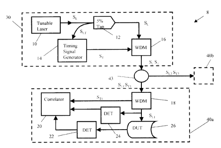
When using a tunable laser as mentioned above, it is. preferred if electronic
circuitry is provided to
correlate an output response for the DU'1' with a particular wavelength of
light propagating through
the device at a particular instant in time.
[03] Systems are currently known drat employ a tunable laser in which the
tuning mechanism
stops at each wavelength to be tested. However, this process takes several
minutes when a large
number (i.e. > 100) of wavelengths are to be measured. The wavelength accuracy
is limited by the
mechanical tolerances of the tuning mechanism.
[04] An object of the present invention is to overcome the shortconungs of the
prior art by
providing a testing device that transmits a modulated variable wavelength test
signal to a DUT to
obtain testing information relating to group delay, while providing an
independent timing information
signal, which is correlated with tire group delay infon~~ation.
1
CA 02417790 2003-O1-30
Doe. No. IU-X51 C:A Patent
SUMMARY OF THE INVENTION
[05] Accordingly, the present invention relates to an apparatus for testing an
optical
component comprising;
(06] a tunable laser for providing a tunable laser signal having a wavelength
that varies with time;
[07] a first modulator for modulating the tunable laser signal producing a
modulated laser signal
defined by frequency, amplitude, and phase;
[08] an information signal generator for generating an infornnation sigmal
having an indicator that
varies with the variations in wavelength of the tunable laser signal;
[09] a test station for receiving the modulated laser signal, and for testing
the optical component
therewith, providing a plurality of test information samples including an
initial and a final phase
measurement of the modulated laser signal taken before and after passing
through the optical
component, respectively, to calculate group delay at various times and
corresponding wavelengths;
and
[10] a correlator for correlating the plurality of test information samples
with the information
signal to deternune the wavelength corresponding to each test information
sample independent of the
specific optical component.
[11] Another aspect of the present invention relates to a method for testing
an optical component,
comprising the steps o~
[12] a) providing a first optical signal that varies in wavelength over time;
[13] b) generating a second signal that has an indication therein related to
variations in
wavelength and time of the first optical signal;
(14] c) modulating the first optical signal providing a modulated optical
signal defined by a
ti~eyuency;
[15] d) testing the optical component with at least a loortion of the
mudulated optical signal to
acquire test iolormation comprising initial and tinal pltase measurements for
calculating group delay
measurements at a plurality of wavelengths;
(16] e) deriving wavelength information relating to the first optical signal,
or a.signal derived
therefrom, from the second signal; and
2
CA 02417790 2003-O1-30
Doc. No, 10-551 CA Patent
[17] f~ correlating the acquired test information with the derived wavelength
information to match
the test information with a corresponding wavelength independent of the
optical component.
BRIEF DESCRIPTION OF THE DRAWINGS
[18] The invention will be described in greater detail with reference to the
accompanying
drawings which represent preferred embodiments thereof, wherein
[19] Figure 1 is a schematic block diagram of a test system wherein a laser
signal and timing
signal generator block provide signals to a test station block for testing an
optical device;;
[20] Figure 2 is a schematic block diagram of a laser signal and timing signal
generator block
providing signals to multiple test stations;
[21] Figure. 3 is a graph showing the output characteristics of a fibre Bragg
grating;
[22] Figure. 4 is a graph showing the output characteristics of an etalon in
accordance with
this invention;
[23] Figure. 5 is a block circuit diagram of an alternative embodiment of the
test system
including circuitry for FM modulation and demodulation of a timing signal;
[24] Figure. 6 is a block circuit diagram similar to that of Fig. 5 and
including means for
deriving synchronization information relating to the scanning laser output
signal wavelength;
[25] Figure. 7a is a detailed block circuit diagram of a circuit for deriving
synchronization
information and for modulating the scanning laser output signal with
wavelength information;
[2fi] Figure. 7b is a graph of two filters output responses depicting
wavelength versus
amplitude;
[27] Figure. 8 is a detailed block circuit diagram of an alternative circuit
for deriving
synchronization information and for modulating the scanning laser output
signal with wavelength
infornation;
[28] Figure. 9 is a schematic block diagram of an embodiment of a system for
determining the
response characteristics of an optical device of the present invention;
[29] Figure. 10 depicts the optical spectrum at an RF detector of the present
invention for an
example condition of the modulation frequency;
3
CA 02417790 2003-O1-30
Doc. No. 10-551 CA Patent
[30] Figure 11 depicts the optical spectrum at an RF detector of the present
invention for the case
of three acquisition points;
[31] Figure 12 depicts the relationship between a desired signal spectrum and
a synthesized signal
spectrum of the present invention;
[32] Figure 13 illustrates empirical group delay curves for measurements on a
NIST HCN test cell
using a low modulation frequency;
[33] Figure 14 illustrates empirical group delay curves for measurements on a
NIST HCN test cell
using a high modulation frequency;
(34] Figure 15 illustrates empirical lnoup delay curves for another set of
measurements on a NIST
HCN test cell using a high modulation frequency;
[35] Figure 16 represents a flowchart according to a method of the present
invention for
calculating the equivalent group delay measured at an arbitrary effective
modulation frequency; and
[36] Figure 17 represents the steps in a method of the present invention for
synthesizing an
effective modulation frequency in deterniining a group delay response
characteristic of an optical
component over a sample optical spectrum.
DETAILED DESCRIPTION
[37] With reference to Figs. l and 2, a basic test system 8 for measuring
insertion loss at
various wavelengths is illustrated, wherein a first block 30 of optical
circuitry and components
provides a variable wavelength optical signal for launching unto a Ul1'f 2(i
within a second block 40a.
In the first block 30, the variable wavelength optical signal in the form of a
tunable laser signal Sl" is
combined with a timing signal S~~ for determining wavelength information
relating to the tunable laser
signal S~. The purpose of separating the circuitry into these two blocks 30
and 40a is to isolate and
separate two primary functions: firstly, that of producing a variable
wavelength optical silmal S,, with
an associated timing signal S~~ for providing timing information relating to
the variable wavelength
optical signal S,, and secondly, the function of testing the device or
component of interest along with
providing the necessary circuitry for doing so in response to the two signals
S,, and ST. Furthermore,
the separation into these two blocks has significant cost advantages as well.
For example, by using a
splitter 43 to split the variable wavelength optical signal S,, along with its
corresponding timing signal
S, into two same signals, another test station 40b identical to block 40a can
be provided with test and
timing signals. Since the most costly part of the entire system 8 is in the
block 30 containing the
4
CA 02417790 2003-O1-30
Doc. No. 10-551 CA Patent
tunable laser, this system obviates the requirement of providing duplication
of the tunable laser to
provide test signals to two or more separate test stations.
[38] Referring now in more detail to the system 8, block 30 includes a tunable
laser 10
capable of being tuned over a wavelength range of interest from a first
wavelength )',, (e.g. 1520nm)
to a second wavelength T,~ (e.g. 1570nm). 'The tunable laser 10 repeatedly
varies its output starting at
~,~ increasing continuously to ~. After reaching ~" the laser returns to ~A
and continues from A,~
again. I~huS tltc laser sweeps acruss th a wamlength rang., and mntinucs
reputedly. A 5'%~ tap 12
receives the output signal S, front the laser 10 and passes ~°/~ S,v,-
to a timing signal generator 14,
while passing 95% of the optical signal SL onwards to a means 16 of combining
this signal with a
timing signal S~,~. Coupling ratios other than the 5/9~~ ratio described above
can alternatively be used.
From the small portion 5~,- of the output signal S, , the timing signal
generator 14 determines when the
signal Sr is at a predetermined wavelength, for example, when its wavelength
is AA. Then the timing
signal generator 14, generates the tinting signal Sr, which indicates that the
signal S~ is at a
wavelength of A,,~. At a subsequent time when the laser wavelength reaches the
next wavelength of
interest ~~ + 0'~. (e.g. 0~=O.Olnm) a subsequent pulse in the timing signal
5,~ is sent indicating a
wavelength of ~., + A~, (e.g. 1 X20.01 nm). As both of the signals SL and S~
are combined by a
coupling means 16, e.g. a WDM filter, care is taken to ensure that the timing
signal St~ is at a
wavelength that differs from the signal S,_ so that the data content of the
signal SL is not affected.
Essentially, the tinting signal ST serves as a marker or indication which can
be used by the block 40a,
and more particularly the means for deterrninin~; wavelength information 20 to
calibrate the
wavelength of the signal S,. at specitic times cowesponding to the tinting
signal S~-. C.'onveniently a
splitter 43 is provided to split the signals S, and 5, into other signals,
e.g. 5, , and 5.,,, S,,=and 5,~, 5,,,
and S-,-,, that can be routed to one or more other test statiom, e.g. 40b,
40c, 40d (only one of which is
shown). Of course alternatively, the tuning signal could be an electrical
signal distributed by
electrical means.
[39] The second block 40a includes means in the form of a wave division
multiplex (WDM)
filter 18 for separating the composite signal 5~., and S~-, into two separate
signals. The signal ST, is
provided to the means for determining wavelength information 20, which also
receives information
from detectors 22 and 24. Of course several detectors 22 can be included for
simultaneously detecting
the output of a mufti-output DUT such as a WDM filter. A large fraction (e.g.
90%) of the signal S~,
output from the filter 18 is provided to the D1JT 26; a small portion (e.g.
10%) is provided to the
detector 24. 'The output signal from the DUT 26 is directed to the detector
22. In operation the
detector 24 relatively deternvines the intensity of the input signal to the
DUT 26 and provides this
information to the correlator means 2(1. ~fhe actual intensity, or power,
measured at the output of the
DL.,'T 26 is provided by the detector 22 to the currelaror means 20. Thug the
correlator means 20 can
CA 02417790 2003-O1-30
Doc. No. lU->jl CA Yatcnt
calculate the loss through the DUT 26 and can determine the corresponding
wavelength of the signal
Sr for that particular loss calculation, in dependence upon the timing signal
Sr. Since the timing signal
S r indicates the instant the signal Sr is at a wavelength of ~,~, a
determination can be made as to the
wavelength of the signal S,_ at other instants in time. An embodiment for
realizing this function will be
described in more detail with reference to Fig. 2.
[40] Referring specifically to Fig. 2, which illustrates a preferred
embodiment of the timing
generating circuit 14, a small portion of an output signal S,, of the tunable
laser 10 is tapped by 5%
optical taps 12a 12b artd 12c, for providing three tap signals S,,-ra, S~Tb
and SL~r~ that are provided to
the timing signal generation circuit 14. Vl.'ithin this circuit 14, a fixed
etalon 31, a fiber Bragg grating
(FBG) 32 and electronic circuitry 33 provide a means of generating a pulsed
modulation signal SM
comprising a train of pulses having ~)L (e.g. 0.01 nm) increments in
wavelength of the signal 5,.. 'the
first pulse in the train of pulses, derived t'rom the output of the FBG 32 and
the output of the fixed
etalon 31, corresponds to the signal S, being at a wavelength of ~,~; the
second pulse corresponds to
the signal Sr being at a wavelength of ~,, + Di~; the third pulse corresponds
to the signal S,_ being at a
wavelength of ~,~ + 20~, and so on, and the last pulse in the train of pulses,
corresponds to the signal
S,. being at a wavelength of ~. Since the input signal S,;r~ to the fixed
etalon 31 varies in wavelength,
and the etalon 31 is selected to have a free spectral range hSR of; for
example, 1.25 GHz or about
0.01 nm (i.e. equal to 47~),_within the range of ),,,~ to >43, the output
signal of the fixed etalon 31 is a
periodic signal. Fig. 4 shows the desired output characteristic of the etalon
31. 'Che distance between
etalon reflective surfaces is calculated as follows:
(41] Etalon FSR[nm]= -/2nd
[42] Etalon FSR[GHz]= c/2nd
[43] where c= the speed of light; n= the refractive index of the material
between the
reflective surfaces; and d= the distance between etalorl reflective surfaces.
[44] The FBG 32 is designed to reflect the input signal when its wavelength is
1520 nm, thus
providing an indication to the circuitry corresponding to a starting point, in
the train of pulses. This is
illustrated in Fig. 3 where at the threshold transmission level, i.e. the
start, is indicated to be at 7~,,. The
electronic circuit 33 in response to the periodic output from the etalon 31
and the indication of when
the signal Sr is at a wavelength of 1~A, generates the modulation signal SM
that is provided to a 1310
nm laser 34. In response to the signal SM the laser generates a train of
pulses, at a wavelength of 1310
nm, spaced apart in time corresponding to 0~. wavelength increments of the
tunable laser signal Sr.
Thus, the modulation signal is converted to a 1310 nm laser pulsed signal Sr
having a wavelength
significantly different from the signal Sr that varies between ~,, and ~.
Before the signals ST and S,.
6
CA 02417790 2003-O1-30
Doc. No. 10-551 CA Patent
are combined, the signal S~ is amplified by an erbium doped fibre amplifier
(EDFA) 15. The EDFA
15 may be necessary to ensure that there is sufficient optical power at each
test station to perform the
loss measurement on the DLJT. A tunable filter 17 tracks the laser wavelength,
transmitting the laser
signal but blocking the spontaneous emission of the EDFA or laser at
wavelengths other than the laser
wavelength.
[45] A wavelength division multiplexor 16 combines the amplified signal Sc,
and the signal S-r
into a composite signal Sc.ST that is fed to a 1 by 8 sputter 43 thereby
providing 8 test signals. Thus, 8
test stations 40a, 40b . .. 40h can be provided at different locations within
a building, with the required
signals and signal information with which to test optical devices. Using the
device shown in Fig. 2, it
takes approximately 1 second to test a DL IT at a plurality of wavelengths
fiom, for example, 1520 nm
to 1570 nm in increments of about O.Olnm, which corresponds to approximately
5000 data points.
[46] In the circuit 14 of Fig. 2, an etalon 31 is used as a means of providing
a periodic signal
as the input signal sweeps from ~A to ~. Of course the etalon 31 may be
substituted with other
suitable interferometric means. Further the FBG 32 is used as a means of
acquiring a relatively precise
indication of its input signal being at ~;~. Once again, various other means
can be envisaged for
indicating when the input signal is at ~A or any other reference wavelength.
The fixed etalon 31 and
FBG 32 have been chosen in the preferred embodiment after considering cost and
availability.
Preferably, temperature stabilization means 29 are provided to ensure that the
output of the
characteristics of the etalon remain as constant as possible.
[47] The timing signal S, need not be combined with the tunable laser signal
Sc.. Instead a
second optical fiber, or a wire, can be use to transmit the timing signal to
each test station. The signals
are combined in the preferred embodiment to simplify the distribution of the
signals among the test
stations or, alternatively, the tunable laser itself can be modulated to
transmit the timing signal.
[48] The laser signal S,, can be distributed to many more than 8 test
stations. The limiting
factor is that sufficient optical power be present at detectors 22 and 24 to
perform the loss and group
delay measurement. If necessary, the laser signal S, could be split after 17,
and re-amplified and split
again. In this way an unlimited number of test stations can operate from one
tunable laser (with
multiple timing signals S~ provided.)
[49] In Fig. 2 an optional polarization state controller 23 is shown teat
imparts a polarization
state to the laser signal S~_ transmitted to the DU'T. By using this
controller 23, the system can
additionally measure polarization dependent loss (PDL) at each wavelength. The
controller 23 is set to
one of 4 polarization states and one wavelength sweep is made, measuring the
loss of the DUT at each
wavelength for that particular state of polarization. 'fhe controller 23 is
then set to the second
7
CA 02417790 2003-O1-30
Doe. No. 10-SSl CA Patent
polarization state and a second wavelength sweep is made. At each wavelength,
4 polarization states
can be used to calculate the average loss (over all polarization states) and
the PDL. A system and
method of measuring polarization dependent loss, onto which the implementation
just described is
based, can be found in United States Patent 5,371,597, issued December 6, 1994
to Favin et al. The
controller 23 can be placed directly after the tunable filter 17, thereby
further economizing and
obviating the need to have a polarization state controller 23 at each station.
[50] Referring now to Fig. 5 an alternative embodiment of the present
invention in which the
tunable laser signal S,, is modulated with the timing information instead of
using a separate timing
signal S,- A tunable laser 50 has a port 53 for receiving or providing a
synchronization control signal
and an output port 51 for providing a variable wavelength optical signal in
the form of a tunable laser
signal 5,,. A frequency synthesizer 55 is responsive: to a synchronization
control signal provided by
the tunable laser 50. Upon receivin~; a start pulse, the frequency synthesizer
55 begins providing a
modulator 57 with a frequency synthesized signal for modulation with tunable
laser signal S~, thereby
providing an encoded or frequency modulated laser sign<cl 5,.~, in the form of
a frequency ramp
indicative of the varying wavelength oh tl~e laser sie;nal S, . The signal
S~h~ is then provided to a 1 xN
sputter 60 having outputs 60a to 60n. As is shown in tigure 5, the output 60a
is provided to a device
under test (DUT) 62 after which the output signal having propagated through
the DUT 62 is analyzed.
The signal is first demodulated removing the critical wavelength information
or instantaneous
wavelength signature, and retrieving the relevant test information from the
demodulated signal S~.
Alternatively, the signal SAN, can be demodulated prior to being provided to
the DUT 62. In another
preferred alternative, demodulation would not be required and the wavelength
information encoded in
the modulated signal would be detected, for example by a frequency resolved
detector 64 that
includes a frequency counter that measures the instantaneous frequency.
Alternatively, a local
oscillator and a mixer can be used to convert the modulated frequency to a
baseband voltage signal.
[51] In Fig. 6 means 56 are shown disposed between the laser 50 and the
frequency
synthesizer 55 for deriving and providing wavelength information to the
frequency synthesizer 55
from a signal provided by the tunable laser 50 that corresponds in wavelength
to the signal Sc..
[52] Refen-ing now to Fig. 7a a portion of the system shown in Fig. 6 is
illustrated in greater
detail. At the output of the scanning laser 50, a small portion S,_, of the
signal S~ is extracted by a tap
coupler 70. Two matched filters 72a and 72b are disposed to receive a same
portion of the tapped
signal S,_,- from a 50:50 splitter 71, and two detectors 74a and 74b
respectively are disposed to receive
output signals from the tilters 72a and 72b. Regions of the filters having
opposite (negative and
positive) slopes are used. A differential amplifier 76 is electrically coupled
to receive output signals
from the detectors 74a and 74b and to provide a si~;nal to a modulator 57 that
is proportional to the
8
CA 02417790 2003-O1-30
Doc. No. 10-551 CA Patent
instantaneous wavelength of the signal Sr,. If required, a linearizing network
78 may be disposed
between the differential amplifier 76 and the modulator 57.
[53] Fig. 7b illustrates the output response of the two optical filters 72a
and 72b and the
region of the filters between the two vertical dashed lines shown that is used
to achieve the advantages
of this embodiment.
[54] In operation, the circuit of Fig. 7a works in the following manner. The
signal Sir is
tapped from the tunable laser output signal S,, and is split substantially
equally between the two filters
72a and 72b. The power detected by detectors 74a and 74b is provided to the
differential amplifier 76,
which provides an output signal that is substantially proportional to the
wavelength of the signal S,_.
This output signal may be linearized if required and then provided to a system
to modulate the
wavelength proportional sigmal with the signal S~. This modulated swept laser
signal SAM, which
includes its near instantaneous wavelength information, is then provided to a
device under test.
Alternatively, as was heretofore described, the wavelength information can be
multiplexed onto
another optical carrier at an alternative wavelength using either digital or
analog modulation
techniques.
[55] Turning now to Fig. 8 a circuit providing electronic synthesis of
wavelength information
is provided to communicate nearly instantaneous wavelength information of
swept or changing signal
Sr, to an optical receiver not shown. In this embodiment the signal S~ is
tapped and the tapped signal
5,,~ is provided to a Fabry-Perot etalon 80 that generates optical pulses to a
detector 82. The free
spectral range of the etalon must be selected so as to include peaks at a
plurality of tunable
wavelengths of interest. An electronic counter 86 counts the number of pulses
from the known start
of a wavelength scan. A frequency synthesizer 88, in response to the counted
value in the counter 86,
converts the number of pulses stored by the counter into a nearly
instantaneous frequency
corresponding to the tiequency ul~ the signal 5~ . As described heretofore,
this signal can be used to
modulate the swept signal S~ via a modulator 83. Alternatively, as shown in
broken line in Fig 8, the
wavelength information can be fed to a laser 85 to produce an optical signal
ST, which can be
multiplexed onto the same optical carrier by a WDM filter 87 at an alternative
wavelength or onto
another optical carrier (not shown) using either digital or analog modulation
techniques.
[56] Another embodiment of the present invention for determining the response
characteristics of an optical device 26 is represented in Figure 9. The
response characteristics of the
optical component can include insertion loss, PDL, group delay and
differential group delay
measurements at a series of wavelengths over a sample optical speckrum. In a
manner similar to that
described for the embodiment represented in Fil;ure l, a tunable laser 10
outputs a sweeping
wavelength laser signal S,. that is combined with a tinning signal ST. Before
being multiplexed with
9
CA 02417790 2003-O1-30
Doc. No. 10-5~1 CA Patent
the wavelength identification information contained in ST via WDM means 16,
the laser signal Sc is
amplitude modulated by an optical modulator 92 as is done in the well known
conventional
modulation phase technique. In a preferred embodiment, the modulation
frequency f;", as generated
by a radio frequency (RF) source 90 is adjusted to match the frequency
increments of the timing
signal as described below. Additionally. bet«re being combined with ST the
polarization of S,.M can
be controlled by an optional pol~~rization controller 200, which applies a
polarization state to the
signal S,.M.
[57] A test signal comprising the sweeping signal S,,~1, modulated, optionally
polarization
conditioned and combined with the tithing signal S~r is supplied, by block 30
(i.e. the test signal
source) to one or more measurement stations via a sputter 43. A measurement
station 40a recovers
the timing signal Sr via a WDM filter 18 and supplies, via a tap 210, a
portion of the sweeping signal
S,,~ to an amplitude detector 124 that outputs a reference amplitude. An
additional portion of the
sweeping signal S~, is used for reconstructing a reference RF signal via a RF
detector 96. The
remaining portion of the sweepin;; signal St.~, is applied to a DUT 26. An
output of the DUT 26 is
split, via a tap 220, and applied to an amplitude detector 122, to output a
signal amplitude, and to an
RF detector 9:1, to extract an RF signal. ~Che RF signal plus the reference RF
signal are input to a
phase detector 98, that outputs tlo. relatme phase difference (i.e. group
delay measurement) between
the sweeping signal S,. input to and the signal output from the DUT 26. The
reference amplitude, the
signal amplitude and the phase difference are captured and correlated with the
wavelength timing
signal by a wavelength correlator 120 thereby determining and capturing the
insertion loss
measurement and group delay measurement versus wavelength over a series of
wavelength
(frequencies) sweeps by the signal S~.
[58] The use of the an uplitude detectors 122, 124 and the associated signal
taps 210, 220 as
represented in Figure 9 is not required as the RF detectors 94, 96 can be used
to obtain amplitude
information as well as phase information. 'hhe previously described embodiment
of figure 9, with
separate amplitude and RF detectors, allows for the amplitude detectors 122,
124 to be of a low
frequency type optimized for the requirements of insertion loss measurement
and for the RF detectors
94, 96 to be optimized for requirements of low noise phase measurement.
[59] As an alternative (not illustrated) to the use of separate amplitude and
RF detectors, a
single detector can be used in con~unetion wUh a sumplc: electrical coupling
network (similar to a
cross-over circuit used in a multi-driver loud speaker) to pass the low
frequency average photocurrent
to an amplitude detection circuit while directing the KF photocurrent to a
high-frequency circuit. The
use of a single detector in conjunction with a. simple electrical coupling
network provides features
similar to the embodiment of Fig. 9 comprising separately optimized RF
detectors 94, 96 and
,~0
CA 02417790 2003-O1-30
Doc. No. 10-551 CA Patent
amplitude detectors 122, 124, while comprising less optical components
resulting in higher signal
levels at the (photo) detectors.
[60] Although not illustrated in Figure 9, in the case of a multi-channel
output DUT 26,
each additional output can be simultaneously measured using an additional set
of components
comprising a tap 220, an RF detector 94 and an amplitude detector 122 for each
additional output.
The outputs of the additional RF detectors 94 and the additional amplitude
detectors 122 are input to
the phase detector 98 and the wavelength correlator 120, respectively, in
order to determine and
capture multiple gr-ottp delay and insertion loss measurements.
[61] fhe spUter 43 allows the test system of the present invention to be
capable of
supporting multiple measurement stations in parallel. This provides a
capability to test many DUT 26
in a single wavelength sweep, while requiring only one tunable laser 10,
optical modulator 92 and
polarization controller 200.
[62] The optional polarization controller 200 allows for the basic measurement
of insertion
loss and group delay versus wavelength to be captured over a range of
polarization states. The
polarization controller 200 is capable of applying a polarization state using
a method well known in
the art - for example, a polarizer and a ~~4 retarder plate followed by a a/2
retarder plate. Polarization
Dependant (insertion) Loss (PDL) and Differential (polarization dependent)
Group Delay (DGD) can
be measured using the "All-States" approach, in which the group delay and
insertion loss are captured
at multiple polarization states. The PDL is given by:
[63] PDL = IL",~r - IL",;"; where IL",;,r and II_",;" are the maximum and
minimum Insertion Losses
(IL) measured over the range of polarization states respectively.
[64] While DCiD is given by:
[65] DGD = GD",ax - GD",;"; where GDma, and GD",;" are the maximum and nunimum
Group Delay
(GD) measured over the range ol'polarization states respectively.
[66] In general, the "All-States" technique requires many scans because of the
number of
polarization states required for accurately determining the minimum and
maximum conditions. A
much more efficient approach can be achieved by generating a specific
combination of four
polarization states, known as a Mueller set, to calculate PDL as described in
US Patent 5,371,597,
Favin et al, issued December 6, 1994. An analogous four-state technique for
DGD has been described
in "Modulation phase-shift measurement of PMD using only four Launched
polarization states: a new
algorithm", P.A. Williams, ELECTRONICS LETTER, Vol. 35, No. 18, September
2°d, 1999 is
summarized as follows. By illuminating a (DUT) with linearly polarized light
at 0°, 45°, 90° and
1.1
CA 02417790 2003-O1-30
Doc. No. 10-551 CA Patent
circularly polarized (circ) light, and by measuring the phase of the light at
the output of the DUT for
each of the aforementioned states of polarization we obtain the phase signals
~, ~ ,~s, ~ y~ and ~ ~;,~
respectively. From these phase sigmals we can then calculate an average group
delay
~Po + ~P9o ~ ;
~GD)=2 _ 2 ;2
and a differential goup delay
DGD = - ] 2 tan-' ~tan2~~p~ - ~~ + lanZ~~p4~ - ~~ + tan2~~p~,,.a - d~~~~
2
where f is the RF modulation frequency and Q~ is the polarization-independent
phase offset.
[67] In order to calculate the goup delay, the tunable laser signal S,, is
modulated in amplitude
with a sinusoidal wavefonn at a radio/microwave frequency f"" typically in the
range of 100 MHz to 3
GHz. Phase measurements ~,, ~, ~,,... are recorded at discrete wavelengths ~,,
~Z, ~3. ...
corresponding to optical frequencies f,, f~, f,, .... The phase is a relative
measurement, and in this
case the frame of reference is the RF signal applied to the optical modulator
92. The correlator 120
can then calculate the group delay by the following equation:
[68] Group Delay; (ps) _ ~' - x 10 ~''
3G0 f,",
[69] In which ~ is in degrees and f", is in Hz.
[70] The above-identified group delay calculation is effectively an average of
the group delay at
exactly wavelength ~;. For a given accuracy and resolution of phase
measurement, the group delay
resolution and accuracy can be improved by increasing the RF modulation
frequency f",. The
improvement in goup delay comes at the expense of wavelength resolution, since
the spectral width
of the optical signal applied to the DUT' is broadened proportionately to f",.
A solution to this problem
is to use a frequency adjustable RF signal generator and phase meter, e.g. in
the form of a single
electrical network analyzer, which enables the user to trade-off goup delay
resolution against
1 ?.
CA 02417790 2003-O1-30
Doc. No. 10-551 CA Patent
wavelength resolution. As a consequence, the optical detectors 96 and 98 would
have to have wide
bandwidths, which adds to their expense and results in inferior signal to
noise ratios relative to
receivers optimized for a small range of lower frequencies. In another
embodiment of the present
invention detailed below, the benefits of a variable modulation frequency f",
are achieved without the
need for widely tunable, high frequency RF equipment for the optical modulator
92 and phase
detector 98.
[71] Figure 10 illustrates an example condition for the modulation frequency
f",. A
sinusoidal signal 300 at the top of the figure represents the wavelength-
tinting signal ST, for example,
derived from an etalon being interrogated will a wavelength-sweeping optical
source. The horizontal
axis represents both optical frequency and time, which are linearly related
for a uniformly sweeping
source (the wavelength is assumed to be increasing with time in this figure)
[72] The timing signal 5~ from the etalon is periodic in optical frequency
with the
following well-known frequency:
[73] frsa=2*n*d / c
[74] Where c is the speed of light, n is the refractive index and d is the
physical spacing
between the etalon's reflective surfaces, which is essentially constant.
[75] A squared waveform 310 represents a digital signal derived from the
timing signal S,
that is useful for visualizing the timing, where for the purpose of
illustration the rising edges can be
considered to be the instances in time when phase measurement acquisition
occurs.
[76] The ellipses 320 depict the optical spectrum at the RF detector 94 at
instances in time,
t, to t5, effectively five spectral snapshots. The spectra each contain a tone
at a center wavelength (~,
through ~s) as well as an upper and lower side tone separated from the center
tone by the modulation
frequency f", as represented by the upwardly pointing arrows. 'The upper side-
tone of one sample
occurs at the identical wavelength (optical frequency) of the lower side-tone
of an adjacent sample
when the following condition holds:
[77] f", = frsa / 2
[78] For f", > frsR / 2, the optical spectrum becomes wider than the sample
period and the
wavelength resolution of the group delay measurements degrades, while if f", <
fFSa / 2 the optical
spectrum is not fully sampled.
[79] The measurements acquired at successive (center) wavelengths (i.e.
snapshots) can be
averaged to synthesize, i.e. to give a result similar t~ the use of, a higher
value of l;", since the phase
13
CA 02417790 2003-O1-30
Doc. No. 10-551 CA Patent
contributions from the upper side-band of one acquisition are cancelled by the
equal but opposite
phase contributions of the lower side-band of an adjacent acquisition.
Averaging "n" successive
snapshots along the wavelength (optical frequency) axis results in an
effective modulation frequency
given by:
[8U1 (f")~rF = n * f"
[81] with the effective measurement wavelength given by the mean of
wavelengths
[82] OFF = mean (~;)
[83] Figure 11 illustrates an example case of three acquisition points
(snapshots) with
ellipses 320 depicting the optical spectrum at the RF detector )4. Applying
the technique described
above, the three successive snapshots can be averaged resulting in a single
equivalent snapshot 330
with an effective modulation frequency (f,")Fr,: equal to 3 * f", and an
effective (center) wavelength of
~4,rr equal to ~~ (i.e. mean (~,, ~, A3)).
[84] This technique can be extended to obtain values (f,")rrr that are non-
integer multiples
of t;" by using weighting functions instead of a simple multi-point average,
allowing any effective
modulation ti~equency greater than 1", to be synthesized.
[85] To generalize to a non-integer relationship between f;" and (t;") ,.,,:
the emulated
sidebands can be located at an arbitrary optical frequency that lies between
two integer multiple
frequencies (e.g. (f,")HFr =(2n+1)f,", and (2n+3)f,",) by using linear
interpolation.
[86] Referring now to Figure 12, the top half of the figure, labeled
"Desired", depicts a
signal 400 with an arbitrary modulation frequency, farbin~rY with no fixed
relationship to f",. The
bottom portion of the figure, labeled "Synthesized", is constructed from
multiple signals, an upper
signal 410 represents the largest odd number integer "2n+1"' multiple of f",
which is smaller than
tarbitrarv~
[87] The bottom signals 420, 430 represent the spectra of the two next
adjacent samples.
The frequency f~~~ is the fractional difference such that:
~] farbitrarv = (2n + 1 ) x f", + ffrac
[89] By the well-known technique of linear interpolation between samples, the
correct
weighting of the fractional samples of the measured RF phase to be used in
numerical processing is
given by:
14
CA 02417790 2003-O1-30
Doc. No. 10-X51 CA Patent
0] W - f~~~ + (2f",) = ( farb;nan. -12n + 1 ) x f",) ~ (2f",)
[91] By rearranging the above equation the etTective modulation frequency,
f~b;tr~., can be
expressed as:
[92] faa;~~« _ (2n + 1 + 2W ) f",
[93] Figure 16 represents a flowchart for a method for calculating, by way of
a weighted
average, the equivalent phase measured at an arbitrary effective modulation
frequency according to
the method of the present invention. 'I he first step 500 is to determine
'2n+1' the integer value of the
quotient of f~~,,;n,~~ and t;". 'fhe value of '2n+1' represents the largest
integer multiple of f", that is less
than F;,rn;,r~a. The next step 510 is to calculate 'W' the weighting
coefticient to be applied to the
component represented by the difference between ts,.h;";"~, and '(2n+1) *
f",'. Using the linear
intezpolation method the weight 'W' is thc: difference between ta~;~~y and
(2n+1) * f"" i.e. (f~b;a~y -
(2n+1) x f;"), and the weight of a standard measurement interval (2 * f",).
The last step 520 is to
calculate the weighted average group delay RF' phase for an effective
modulation frequency of fe~b~tr~,
using the linear interpolation method resulting in:
(W * RFPh ase(-(n + 1 )) + W * RFPhase(+(rx + 1)) + ~+" RFPhase(i))
RFPhaseAvg = - -
(2ia-~1+2W')
[94] Where RFPhase (-(n+1)) and RFPhase (+(n+1)) correspond to the left-most
and right-most
samples in Figure 12 and the change in group delay, RF phase, is approximately
linear over a
frequency span of 2 x f",. The summation of group delays, RFPhase(i), is over
all of the intermediate
(2n +1) samples.
[95] Measurements have been made using the method of effective modulation
frequency
synthesis described above and results are present here. The data comes from
two sources, both for
measurements on the same National Institute of Standards and Technology (NIST)
hydrogen cyanide
(HCN) cell, also known as NIST Standard Reference Material 2519, as follows:
[96]
( 1 ) Testing on an Advantest Q7750 optical network analyzer:
- Modulation freq: 200MHz.
Modulation fi-eq: 2UHz.
CA 02417790 2003-O1-30
Doc. No. 10-551 CA Patent
(2) Testing on a 3DS Uniphase swept wavelength ::hromatic dispersion (SWS-CD)
optical
component test system:
- Modulation Freq: 192MHz
[97] Figure 13 illustrates empirical soup delay curves from measurements on
the NIST
HCN cell using a low modulation frequency. A trace 600 in the graph represents
the measurements
taken by the Advantest 775() with a f", of 200MHz. A trace 610 in the graph
represents the
measurements taken with SWS-CD with a f", of 192MHz. It can be seen from the
graph that the
results for the two measurement sources with approximately the same low
modulation frequency
(200MHz vs. 192MHz) are highly correlated. 'this indicates that for the same
(or approximately the
same) modulation frequency both the Advantest Q7750 and the SWS-CD generate
similar results.
[98] Figures 14 and I S illustrate empiric<~l ~n-oup delay curves .for the
NIST HCN cell
using a high modulation frequency. In both figures 14 and 15 a trace 620 in
the graph represents the
measurements taken by the Advantest 7750 with a f", of 2.(IGHz. Using the
synthesized effective
modulation frequency method with the SWS-CD at a 1~", of 192MHz, effective
modulation frequencies
of 1.92GHz and 2.11GHz can be achieved by averaging over 10 and I1 sample
measurements
respectively. These two effective frequencies of modulation are close
approximations for a f", of
2.OGHz and effectively bracket that f",. In figure 14 a trace 630 in the graph
represents the
measurements taken with SWS-C'D with a f", of 192 MHz, averaged over 10 sample
measurements,
i.e.GD2(i)=(GD 1 (i-5 )+GD 1 (i-4)+GD 1 ( i-3)-.-GD 1 (i-2)-rGD 1 ( i-1 )+GD 1
(i)
-GDI(i+1)+GD1(i+2)+GDI(i+3)+CiDI(i+4))/10 for a (f;"),.;,:,: of 1.92(lHz. In
figure 15 a trace 640 in
the graph represents the measurements taken with SWS-CD with a f", of 192MHz,
averaged over I l
sample measurements (i.e. GD2(i)= ( GD1(i-S)+ GDI(i-4)~GD1(i-3)+GDI(i-2)+GD1(i-
1)+GD1(i)+GD1(i+1)+GD1(i+2)+GD1(i+3) +GD1(i+4)+GD1(i+5))/11) for a (f,")sFF of
2.IlGHz. It
can be seen from the graphs in both Figures 14 and 15 that the results for the
two measurement
sources with approximately the same high modulation frequency (2.OGHz) or
effective modulation
frequency ( 192GHz and 2_ 11 GHZ) are highly correlated. These results
validate that the method of
effective modulation frequency synthesis can provide Group Delay measurements
that are similar to
those resulting from a traditional G1) measurement technique for a given
modulation frequency while
using an actual f", that is substantially lower.
[99] In comparing the low t;" results in Figure 13 with the high f", results
in Figures 14 and
15 it can be seen that in the case of both an actual high f", and a high
effective f", a significant
improvement in group-delay noise and resolution has been gained, although at
the expense of
16
CA 02417790 2003-O1-30
Doc. No. 10-551 CA Patent
wavelength resolution. It is also clear that the use of a synthesized,
"effective" modulation frequency
is both useful and representative of using the corresponding actual modulation
frequency.
[100] The method of the present invention provides for determining, using the
conventional
modulation phase technique, the group delay response characteristics of an
optical component by
taking multiple, successive spaced-apart (in wavelc;ngth) measurements for a
given modulation
ti-equency t;" and by 'weighted averaging' of the multiple, spaced-apart
measurements, determining a
result substantially equivalent to the result of a single measurement at the
average center wavelength
of the multiple, successive spaced-apart measurements and with an effective
modulation frequency
that is an arbitrary multiple of f",. Thereby, synthesizing the effective
modulation frequency.
[101] Fig. 17 represents the steps in a method of the present invention for
synthesizing an
effective modulation frequency in determining a group delay response
characteristic of an optical
component (i.e. DUT) over a sample optical spectrum. 'fhe tirst step G00 is to
apply a sweeping
wavelength optical signal modulated with a KF signal, such as for example the
test signal output by
block 30 in Fig. 9, to the optical component. Next a series of measurements
are obtained 610 at a
series of equally spaced apart wavelengths swept by the sweeping wavelength
optical signal and that
span the sample optical spectrum. Each measurement includes: a group delay
determined from a
reference phase derived from the sweeping wavelength optical signal and an
output phase derived
from the output signal of the optical component; and a measurement center
frequency representing the
frequency of the sweeping wavelength optical signal when the measurement is
taken. A weighted
average of the group delays included in the series of measurements is
calculated 620 to determine the
group delay response characteristic. The weights used in the weighted average
relate to the portion of
the sample optical spectrum that is sampled by each of the series of
measurements such that the
synthesized effective modulation frequency is equal to the product of the sum
of the weights and the
frequency of the RF signal.
[102] Of course numerous other embodiments can be envisaged without departing
from the
spirit and scope of the invention.
17