Note: Descriptions are shown in the official language in which they were submitted.
CA 02418349 2003-02-04
GLASS SUBSTRATE WITH FINE HOLE AND METHOD FOR PRODUCING THE SAME
BACKGROUND OF THE INVENTION
The present invention relates to a glass substrate having
at least one fine hole which serves as a guide hole for mounting
an optical fiber used in the field of optical communication or
S as an ink ejection hole for a printer used in the field of office
automation equipment.
:: board made of a plate-like resin material such as a
nolv~;:.mide-based resin or a fluorocarbon-based resin and provided
with Line thrcugh-holes is used ~,aidely as a multilayer wiring
board for electronic appliance, a head of an ink-jet printer,
a retention mem:oer of an optical fiber array, etc. Each of the
through-holes serves as an electric contact hole in the multilayer
wiring board, as an ink ej ection hole in the head of the ink-j et
printer or as an optical fiber guide hole in the retention member
of the optical fiber array.
Each of the through-holes has a diameter in a range of from
the order of tens of um to about 200 um. A laser beam machine
using a CC laser, a YAG laser, or an excimer laser of KrF or
the lv'~:e is generally used for forming these holes.
Cn the other hand, because glass has a feature to be superior
in chemical stability and heat resistance to resin, a glass
substrate having fine holes formed therein can be adapted for
- 1 -
CA 02418349 2003-02-04
more use purposes . I f the glass substrate is subj ected to laser
machining, there is however a problem that the glass substrate
cracks easil~~ .
As measures to solve this problem, a technique in which
a glass substrate is heated at a temperature of 300°C to 700°C
before laser machining so that the glass substrate can endure
heat shock at the time of laser machining has been disclosed
in JP-A-54-28590.
Further, an example in which silver in an atomic, colloidal
or ionic state is contained in a glass substrate to improve
applicabilit~~ of laser machining to the glass substrate has been
described in JP-A-10-338539.
Although it is possible to form fine holes in a glass substrate
by laser machining, it is difficult to control the diameter of
each fine hole with accuracy of not larger than 1 um.
For example, the accuracy of the hole diameter of a guide
hole for moun=ing an optical fiber used in the field of optical
communication is required so that a clearance for the diameter
of the optical fiber is controlled in the order of 1 um or smaller
to ensure the positional accuracy of the optical fiber. Moreover,
according to Japanese Industrial Standards (JIS), even variation
of larger than 1 um in the diameter of the optical fiber used
is allowed because the accuracy of the diameter of the optical
fiber is defined as ~1 um. It is therefore necessary that the
accuracy of the hole diameter of the guide hole is kept not larger
CA 02418349 2003-02-04
than 1 um relative to the variation in the diameter of the optical
fiber. In laser machining, it is very difficult to adjust the
hole diameter.
L~Ioreover, the hole formed by laser machining is tapered.
Because the small-diameter side having large influence on the
final alignment of the optical fiber is a rear surface side opposite
to a front surface irradiatedwith laser beams, it is more difficult
to control the hole diameter.
L~Ioreover, even in the case where the crack arresting means
is used at the time of laser machining, the boundary portion
between the hole side surface on the small diameter side and
the cor responding substrate surface is apt to be cracked or chipped
because it is difficult to eliminate the influence of heat shock
thoroughl~_~. Hence, when the optical fiber is inserted into the
hole, there is fear that the small-diameter side of the glass
substrate may be chipped and broken pieces may be deposited on
tip of the optical fiber to disturb assembling.
In addition, the inner wall surface of the hole formed by
laser machi:~ing may be denatured or cracked finely by the influence
of heat. j,~Ihen silver-containing glass is used, there is
possibilitvi that silver colloid may precipitate. Hence, there
is a further problem that the function of a product may be spoiled
because glass dust or silver colloid is deposited on a tip of
the cptical fiber when the optical fiber is inserted into the
hole.
- 3 -
CA 02418349 2003-02-04
SUNINL~RY OF THE IN'JENTION
The invention is developed to solve the problems and an
object of the invention is to provide a method for forming a
through-hole in a glass substrate, by which method the hole diameter
of the through-hole is controlled with high accuracy and the
inner wall surface of the through-hole has no layer denatured
by machining.
As a feature of the glass substrate having at least one
fine hole according to the invention, a side wall surface of
the fine hole is connected to each surface of the glass substrate
by a curved surface as a boundary portion between the two. As
another feature of the glass substrate, a layer denatured by
machining is removed from the inner wall surface of the fine
hole and the boundary portion between the wall surface of the
fine hole and each surface of the glass substrate. It is desirable
that the fine hole is tapered particularly in a direction of
thickness of the alass substrate.
Because even the smallest-diameter portion of the fine hole
l s net chipped so that the surface cf the smal lest-diameter portion
is formed as a smoothly curved surface, the hole diameter, for
example, required when the hole is used for holding an optical
fiber inserted into the hole can be easily controlled with high
accurac~.~.
The fire hole according to the invention is produced by:
forming a fine hole in a glass substrate by machining or laser
- 4 -
CA 02418349 2003-02-04
machining; and then applying liquid-phase chemical etching to
surfaces of the glass substrate and the fine hole . On this occasion,
desirably, an etching liquid used in the liquid-phase chemical
etching is either of an aqueous solution of hydrofluoric acid
and an aqueous mixture solution of hydrofluoric acid and ammonium
fluoride.
Laser machining is means adapted for forming a fine hole
in glass . When laser machining is combined with chemical etching
in liquid phase, a fine through-hole having the aforementioned
sectional shape having a hole diameter controlled with high
accuracy can be formed in a glass substrate by machining.
The present disclosure relates to the subj ect matter contained
in Japanesepatentapplication No.P2002-027816(filed on February
5, 2002), which is expressly incorporated herein by reference
in its entirety.
BRIEF DESCRIPTION OF THE DRAWINGS
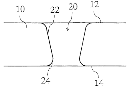
Fig. 1 is a typical view showing the shape of a fine hole
formed in a glass substrate by laser machining.
Fig. 2 is a typical view showing the external appearance
of the fine hole in a rear surface of the glass substrate.
Fig. 3 is a graph showing the relation between etching time
and change of hole diameter in an embodiment of the invention.
Fig. 4 is a typical view showing the sectional shape of
a fine hole in the embodiment of the invention.
~ lg. S is a typical view showing an applied example in which
- 5 -
CA 02418349 2003-02-04
the invention is applied to an optical fiber retention member.
DESCRIPTION OF THE PREFERRED EMBODIMENT
A feature of the invention is that a glass substrate having
fine holes formed by machining or laser machining in advance
is further subjected to etching to adjust the hole diameter of
each fine hole and improve the quality of the inner wall surface
of each fine hole.
Production of a retention member for mounting an optical
fiber array will be described below. A target value of the hole
diameter is set at 125 um which is equal to the outer diameter
of a single mode optical fiber used generally.
First, to form holes by laser machining, a 0.3 mm-thick
glass substrate was modified by ion exchange. The method of
ion exchange was basically the same as described in JP-A-10-338539.
The glass substrate was made of silicate glass containing Si0_
as a main component and further containing A1=0;, B_0:, Na~O, F,
etc. The glass substrate was immersed in a molten salt mixture
containing 50 by mole of silver nitrate, and 50 ', by mole of
sodium nitrate. The temperature of the molten salt mixture was
300°C. The immersion time was '72 hours. By this processing,
Na ions in surfaces of the glass substrate were eluted while
Ag ions in the molten salt mixture were diffused into the central
pcrtion of the glass substrate.
The glass substrate 10 was irradiated with light of the
third harmonic wave (wavelength: 355 nm) of a YAG laser to form
- b
CA 02418349 2003-02-04
a through-hole b~rmachining. On this occasion, the glass substrate
was irradiated with a laser beam having a beam spot diameter
of 130 um and beam power of 39 J/cm-. As a result, there was
obtained a fine hole 20 piercing the glass substrate 10 so as
5 to be shaped like a taper having a diameter of 130 um at a beam
incidence side surface 12 and a diameter of 115 um at a beam
emergence (rear) side surface 14 as shown in Fig. 1 . As an example,
to produce a retention member for retaining an array of 4 X 4
optical fibers, laser beam irradiation was repeated while a stage
10 on which the glass substrate 10 was mounted was moved. Thus,
an array of a ., 4 holes was formed.
6~7hen one of the holes was observed from the beam emergence
side, a large number of chips 30 were found in the boundary between
the i nner wall surface of the fine hole 20 and the rear surface
1 J of the glass substrate as shown in Fig. 2. It was also observed
that the hole wal 1 surface 22 was colored because i t was denatured
by laser machin~_ng.
Therefore, the whole of the glass substrate having the fine
holes formedwas stched in liquid phase according to the invention.
An aqueous mixture solution of hydrofluoric acid and ammonium
fluoride was used as an etching liquid. As an example, an aqueous
solution of 2.5 by weight of hydrofluoric acid and an aqueous
solution of 30 by weight of ammonium fluoride were mixed at
the weight ratio of 1:1, so that the resulting mixture solution
was used as an etching liquid.
CA 02418349 2003-02-04
The change of the hole diameter versus the etching time
in use of the etching liquid at a liquid temperature of 40°C
was as shown in Fig. 3. The hole diameter was measured at the
smallest-diameter portion of the tapered hole, l . a . , at the beam
S emergence side of the glass substrate. The initial value of
the hole diameter before etching was 115 um as described above.
The hole diameter changed rapidly just after the start of etching
but the rate of the change of the hole diameter was reduced with
the passage of time. This was because the beam emergence side
after laser machining was shaped like a sharp angle in section
as shown in Fig. 1, so that this portion was etched at the beginning.
Accordingly, it is desirable that etching is performed up to
a depth sufficient to reduce the etching rate for the double
purposes of forming connection between the wall surface of the
hole and the surface of the glass substrate on the beam emergence
side as a smoothly curved surface and removing tile layer denatured
by machining.
F.lrther, to ma}>e the etching rate as low as possible is
advantageous to accurate control of the hole diameter.
Accordingl ~,~, it is desirable that the hole diameter to be obtained
by laser machining is decided on the basis of both etching time
and etching depth determined by referring to the characteristic
shown in Fig. 3.
Further, because the through-hole formed by laser machining
is tapered as shown in Fig. l, the optical fiber inserted into
_ g _
CA 02418349 2003-02-04
the through-hole is supported by the smallest-diameter portion
of the through-hole. Accordingly, a target value of the beam
emergence side hole diameter formed by laser machining as the
first step needs to be decided so that the hole diameter of the
smallest-diameter portion has a desired value.
In this embodiment, the glass substrate 10 having the holes
formed thus was etched for 10 minutes while the liquid temperature
of the etching liquid was kept at 40°C. As a result, a sectional
shape as shown in Fig. 4 was obtained. The large number of chips
30 in the boundary between the beam emergence side of the hole
and the rear surface 14 of the glass substrate were eliminated
by etching, so that the fine hole 20 was formed to have a curved
sur face 24 . A state in which the layer denatured by laser machining
could be removed from the hole wall surface 22 was also observed.
I5 The hole diameter of the smallest-diameter portion after etching
was 125 Vim. The standard deviation in hole diameter of the sixteen
holes was improved from 2 . 5 um be=ore etching to 1 um after etching.
ig. S shcws an example in whi ch a glass substrate 10 having
an arra~J of fine holes 20 formed therein is mounted as a member
for retaining optical fibers 32. A hole array 40 according to
the invention is used for arranging sixteen single mode optical
fibers 32 as an array of 4 X 4 optical fibers. Microlenses 52
are formed as a mi crolens array 50 in a planar transparent substrate
to sc that the position of each microlens 52 coincides with the
position of a corresponding fine hole 20 in the hole array 40.
_ g _
CA 02418349 2003-02-04
The hole pitch of the hole array 40 is made coincident with
the lens pitch of the microlens array 54 in advance. Hence,
the hole array 40 can be stuck to the microlens array SO easily
while the fine holes 20 are aligned with the microlenses 52
respectively.
The sixteen optical fibers 32 are inserted into the fine
holes 20 respectively in the hole array 40 and fixed by an
ultraviolet-curable resin 60 or the like. When the microlens
array SO is designed appropriately, a collimator array can be
formed so that divergent pencils of rays 70 emitted from the
optical fibers 32 are converted into parallel pencils of rays
72 respecti ~Jely by the collimator array. Light rays propagated
through the optical fibers can be coupled to various optically
functional devices easily by the collimator array.
B=i use of the aforementioned configuration, the process
for assembling an optical system can be simplified greatly compared
with the case where optical fibers are aligned and coupled with
lenses individually to form a plurality of collimators.
Although this embodiment has been described on the case
where the glass substrate is etched with a mixture solution of
hydrofluoric acid and ammonium fluoride, the invention may be
also applied to the case where the glass substrate is etched
with only hydrofluoric acid. Further, a solution such as KOH
or ~IaOH having a function of etching the glass substrate may
be used as the etching liquid.
- 10 -
CA 02418349 2003-02-04
Although this embodiment has been described on the case
where etching is applied to fine holes formed by laser machining,
the method according to the invention may be also effectively
applied to tine holes formed by another means such as electron
beam machining, drilling or sandblasting.
A through-hole formed in a glass substrate by machining
or laser machining is further etched in liquid phase so that
the hole diameter of the through-hole can be controlled with
high accuracy. In the case of a plurality of through-holes,
variation in hole diameter of the through-holes can be reduced.
In addition, a layer denatured by machining can be removed from
the inner wall surface of each hole and the boundary portion
between the hole wall surface and each surface of the glass
substrate.
- 11 -