Note: Descriptions are shown in the official language in which they were submitted.
CA 02423028 2003-03-20
WO 02/25700 PCT/GBO1/04211
-1-
SEMICONDUCTOR DEVICE
AND METHOD OF FORMING A SEMICONDUCTOR DEVICE
The present invention relates to a semiconductor
device and to a method of forming a semiconductor device.
The present invention is particularly concerned with
high voltage/power semiconductor devices which can be used
as discrete devices, in hybrid circuits and in power
integrated circuits and is particularly concerned with
field-effect transistors, such as power MOSFETs, insulated
gate bipolar transistors (IGBTs) and other types of power
devices such as diodes, transistors and thyristors.
For devices designed for use in integrated circuits,
it is preferred that the main terminals (variously called
the anode/cathode, drain/source and emitter/collector) and
the control terminals (termed the gate or base) are placed
at the surface of the device in order to be easily
accessible. The main current flow is between the main
terminals and is therefore principally lateral. Such
devices are therefore typically referred to as lateral
devices. Such devices are often integrated with low-
voltage devices or circuits built in CMOS-type or other
standard planar technologies to form power integrated
circuits. Several high voltage/power devices may be
integrated in the same chip. Isolation is provided between
the high-power and the low-power devices as well as between
adjacent power devices. Two principal isolation
technologies have emerged, namely junction-isolation (JI)
technology and silicon-on-insulator (SOI) technology.
CA 02423028 2003-03-20
WO 02/25700 PCT/GBO1/04211
-2-
In JI technology, a reverse-biased junction is used to
isolate adjacent devices. However, this is in many cases
not satisfactory for power integrated circuits since
minority carrier conduction through the semiconductor
substrate (on which the active part of the device is
formed) can take place and interference between adjacent
devices is therefore difficult to prevent. In addition, JI
bipolar devices (such as the lateral IGBT) also suffer from
parasitic mobile carrier plasma stored in the semiconductor
substrate in the on-state which has to be removed during
turn-off. This decreases dramatically the switching speed
of the devices.
In SOI technology, a buried insulating layer is used
to isolate vertically the top semiconductor layer from the
bottom semiconductor layer and, accordingly, current
conduction is principally restricted to the top
semiconductor layer and there is practically no current in
the bottom semiconductor layer in any mode of operation.
Horizontal or lateral isolation in SOI is typically
provided via trenches which are filled with oxide or by use
of the known LOCOS ("local oxidation of silicon")
isolation. SOI technology offers better isolation than JI
technology because the buried insulating layer prevents
current conduction and plasma formation in the substrate.
High voltage semiconductor devices have incorporated
within the body of the device a high voltage junction that
is responsible for blocking the voltage. This junction
includes a relatively lowly doped semiconductor layer which
withstands the largest portion of the voltage across the
main terminals when the device is in the off-state and
operating in the voltage blocking mode. This layer is
CA 02423028 2003-03-20
WO 02/25700 PCT/GBO1/04211
-3-
commonly referred to as the drift region or layer and is
partially or fully depleted of minority carriers during
this operating mode. Ideally, the potential is equally
distributed along the drift region between the two ends of
the drift region. However, as shown by the 1-D Poisson
equation, for a given doping of the drift region, the
distribution of the electric field has a triangular shape
or, when fully depleted, a trapezoidal shape. Since the
area underneath the electric field can be approximated as
the breakdown voltage when the peak of the electric field
reaches the critical electric field in the semiconductor,
it is obvious that for a 1-D junction, the lower the doping
of the drift layer, the higher the breakdown voltage.
However, for majority carrier devices such as MOSFET types,
known as LDMOSFETs, the on-state resistance of the drift
layer is inversely proportional to the doping of the drift
layer. Since a low on-resistance is desired for a high
voltage switch, it follows that a low doping concentration
affects the on-state performance of the device. In
addition for lateral devices, the critical electric field
at the surface is smaller than in the bulk, adding further
difficulties in designing high voltage lateral devices.
The introduction of the RESURF (Reduced Surface Field
Effect) technique for JI devices allows an increase in the
breakdown voltage of lateral devices through the use of an
additional vertical junction formed between the drift
region and-the semiconductor substrate. Figure la shows
schematically a conventional JI diode using the RESURF
effect. This diode is provided as part of a conventional
lateral power device such as a lateral transistor, LDMOSFET
or LIGBT. Figure 1a also shows the distribution of the
potential lines and the edge of the depletion region during
CA 02423028 2003-03-20
WO 02/25700 PCT/GBO1/04211
-4-
the voltage blocking mode. It can be noted that the drift
layer 1 is fully depleted but the semiconductor substrate 2
is not fully depleted. The potential lines bend as they
drop in the substrate, from the vertical direction towards
the horizontal direction, such that below the high voltage
terminal 3, the potential lines are practically parallel to
the bottom surface 4 of the substrate 2. This is because
the thickness of the semiconductor substrate 2 is
relatively large (typically 300~,m) compared to the vertical
extension of the depletion region from the top surface 5
into the substrate 2 (typically 60~m for a 600V device).
Hence, the semiconductor substrate 2 is not fully depleted
when the breakdown of the device occurs. It is known that
a lateral JI diode can achieve breakdown voltages
equivalent to those of vertical diodes, in spite of the
reduced surface critical electric field. Nevertheless, as
shown in Figure la, even an optimised electric field
distribution using the RESURF concept is far from being
ideal (i.e. rectangular in shape). In addition as already
mentioned, the JI devices suffer from high leakage currents
and very poor isolation, which makes integration within a
power integrated circuit very difficult.
Figure 1b shows a conventional SOI diode which is
typically found as part of a SOI lateral high voltage power
device. The structure can be made using the known wafer
bonding, Unibond or SIMOX SOI technologies. Other
technologies such as Silicon-on-Diamond (SOD) are also
known. Figure 1b also shows the equi-potential line
distribution during the voltage blocking mode. It can be
seen that the potential~lines crowd towards the edges of
the drift layer 1, resulting in a poor RESURF effect.
CA 02423028 2003-03-20
WO 02/25700 PCT/GBO1/04211
-5-
Increasing the thickness of the buried oxide 6 helps to
redistribute the potential lines more evenly at the top
surface 5. However, in general, the breakdown voltage is
still below that of a JI device or JI diode as shown in
Figure 1a. Again, the potential lines in the drift layer 1
and the buried silicon oxide insulating layer 6 below the
high voltage terminal are practically aligned to the
horizontal surface. This is due to the fact that the
semiconductor substrate 2 is not entirely depleted. The
result is that all the potential lines have to crowd into
the drift layer 1 and insulating layer 6 in the case of SOI
and moreover have to align parallel to the insulating layer
6/semiconductor substrate 2 interface. This creates an
uneven distribution of the potential lines at the top
surface 5 which results in high electric field peaks and
therefore lower breakdown voltages. In addition, for SOI
devices, the conservation of the perpendicular component of
the electric flux density D=EE at the top of the
semiconductor layer 1/buried oxide 6 interface limits the
maximum voltage that the buried oxide 6 can sustain before
the critical electric field in the semiconductor layer 1 at
the interface is reached. This vertical breakdown yields a
very strong limitation on the maximum voltage rating
achievable for a given buried oxide thickness.
Thus, in summary, in both JI and SOI devices, the
potential lines have to bend from a vertical orientation to
a horizontal or lateral orientation and the potential
distribution in the drift layer is far from ideal.
Moreover, when a power integrated circuit made in thin
SOI technology comprises at least a half-bridge
configuration, which involves two power devices operating
CA 02423028 2003-03-20
WO 02/25700 PCT/GBO1/04211
-6-
in different modes, the device operating in the high side
mode may suffer from pinch-off of the drift region during
the on-state. This is due to the high electric field in
the drift region caused by the high negative potential
created in the semiconductor substrate with respect to the
potential of one of the main terminals of the high-side
device.
It is therefore apparent that the semiconductor
substrate in the SOI technology is not passive in all
operation modes and its presence results in a poor
distribution of the potential lines during the voltage
blocking mode, which may cause premature breakdown commonly
at the surface of the semiconductor or at the buried
oxide/top semiconductor interface due to vertical
breakdown. The JI approach suffers from very poor
isolation within the power integrated circuit and the
breakdown voltage, although generally higher than in the
SOI devices, is still lower than would be preferred.
For discrete devices or hybrid circuits used in high
voltage or power electronics, it is preferred that the main
terminals have a vertical orientation and are placed at
opposite sides of the wafer (e. g. with the low voltage
terminal at the top and the high voltage terminal at the
bottom). These devices are referred to as vertical high
voltage/power devices. Compared'to lateral devices, the
current flow between the main terminals is principally
vertical and this results in a larger current capability
and a higher breakdown voltage. Such devices are however
difficult to use in integrated circuits. Example of known
high voltage/power devices are DMOS & Trench MOSFETs, DMOS
& Trench IGBTs and Cool MOS.
CA 02423028 2003-03-20
WO 02/25700 PCT/GBO1/04211
_7_
For an optimised trade-off between on-state/
switching/breakdown performance, the vertical devices
require a narrow drift region that is preferably fully
depleted at full voltage blocking. Such a layer may have a
thickness from 6~,m to 180~,m for devices rated from 50 V to
1.2 kV. Commonly the drift layer lies on a highly doped
semiconductor substrate. The semiconductor substrate
however introduces a series of negative effects on the
general performance of the device. First, it introduces a
parasitic resistance, which leads to increased on-state
power losses. Secondly, for bipolar devices with anode
injection such as IGBTs, since the doping of the substrate
is high, to reduce the power losses in the substrate
resistance, the injection from the substrate which acts as
the anode (emitter) of the device is in most cases too.
strong, leading to high transient switching losses and slow
turn-off due to the a large amount of plasma stored inside
the drift region during on-state. Thirdly, the substrate
introduces a thermal resistance which prevents effective
dissipation of heat to an external sink placed at the
bottom of the device. Finally, if vertical devices are to
be used in integrated circuits, the presence of the thick
semiconductor substrate makes isolation between adjacent
devices very difficult.
There have been numerous prior proposals for
increasing the breakdown voltage of semiconductor devices,
particularly power semiconductor devices. Examples are
disclosed in US-A-5241210, US-A-5373183, US-A-5378920,
US-A-5430316, US-A-5434444, US-A-5463243, US-A-5468982,
US-A-5631491, US-A-6040617, and US-A-6069396. However,
none of these prior art proposals has tackled the problem
CA 02423028 2003-03-20
WO 02/25700 PCT/GBO1/04211
_g_
of increasing the breakdown voltage by a detailed
consideration of the electric potential lines in the drift
region.
In WO-A-98/32009, there is disclosed a gas-sensing
semiconductor device. A gas-sensitive layer is formed over
a MOSFET heater which is used to heat the gas-sensitive
layer. The substrate on which the device is formed is
back-etched to form a thin membrane in the sensing area.
It should be noted that the MOSFET heater is a low voltage
device (and as such does not have a drift region) and,
furthermore, the thin membrane is formed below the MOSFET
heater solely to facilitate heating of the sensing area to
very high temperatures and not to affect the field or
potential lines in the device.
US-A-5895972 discloses a method and apparatus for
cooling a semiconductor device during the testing and
debugging phases during development of a device. In place
of conventional heat slugs such as copper, a heat slug of
material that is transparent to infra red.is fixed to the
device. A diamond heat slug is disclosed as preferred. It
is disclosed that the substrate on which the device is
formed can be thinned prior to applying the infra red
transparent heat slug to the device. The purpose of this
thinning of the substrate is to reduce transmission losses
that occur during optical testing and debugging of the
device using-infra red beams. There is no discussion of
the type of semiconductor device to which the heat slug is
applied and there is no disclosure that the device is a
power device having a drift region. Moreover, as stated,
the purpose of the thinning of the substrate and
application of the heat slug is solely to facilitate
CA 02423028 2003-03-20
WO 02/25700 PCT/GBO1/04211
_g_
testing of the device using optical testing and debugging.
This process is carried out during development of the
device. The heat slug is not used during normal operation
of the device.
There have been a number of proposals in the prior art
for semiconductor devices which make use of a so-called
membrane. Examples include US-A-5420458, WO-A-94/22167,
US-A-3689992 and US-A-6008126. In the case of each of
these prior art proposals, the semiconductor device is not
a power device and thus does not have a drift region. In
each case, the membrane arrangement is used to provide for
isolation between semiconductor devices in an integrated
circuit or between regions within a semiconductor device
and/or to remove or lower coupling parasitic capacitances.
In each case, since these are low voltage devices, the
breakdown voltage is virtually unaffected by the membrane
structure.
According to a first aspect of the present invention,
there is provided a power semiconductor device having an
active region that includes a drift region, at least a
portion of the drift region being provided in a membrane
having opposed top and bottom surfaces, the top surface of
the membrane having electrical terminals connected directly
or indirectly thereto to allow a voltage to be applied
laterally across the drift region, the bottom surface of
the membrane not having a semiconductor substrate
positioned adjacent thereto.
According to a second aspect of the present invention,
there is provided a power semiconductor device having an
active region that includes a drift region provided in a
CA 02423028 2003-03-20
WO 02/25700 PCT/GBO1/04211
-10-
layer, the layer being provided on a semiconductor
substrate, at least a portion of the semiconductor
substrate below at least a portion of the drift region
being removed such that said at least a portion of the
drift region is provided in a membrane defined by that
portion of the layer below which the semiconductor
substrate has been removed, the top surface of the membrane
having electrical terminals connected directly or
indirectly thereto to allow a voltage to be applied
laterally across the drift region.
According to a third aspect of the present invention,
there is provided a power semiconductor device having an
active region that includes a drift region, at least a
portion of the drift region being provided in a membrane
having opposed top and bottom surfaces, at least one
electrical terminal connected directly or indirectly to the
top surface and at least one electrical terminal connected
directly or indirectly to the bottom surface to allow a
voltage to be applied vertically across the drift region,
the bottom surface of the membrane not having a
semiconductor substrate positioned adjacent thereto.
According to a fourth aspect of the present invention,
there is provided a power semiconductor device having an
active region that includes a drift region provided in a
layer, the layer being provided on a semiconductor
substrate, at least a portion of the semiconductor
substrate below at least a portion of the drift region
being removed such that said at least a portion of the
drift region is provided in a membrane defined by that
portion of the layer below which the semiconductor
substrate has been removed, and at least one electrical
CA 02423028 2003-03-20
WO 02/25700 PCT/GBO1/04211
-11-
terminal connected directly or indirectly to the top
surface and at least one electrical terminal connected
directly or indirectly to the bottom surface to allow a
voltage to be applied vertically across the drift region.
The said at least a portion of the drift region is
fully or substantially fully depleted of mobile charge
carriers when a voltage is applied across terminals of the
device. In the first and second aspects of the present
invention, the potential lines in said at least a portion
of the drift region are substantially perpendicular to the
top and bottom surfaces of the membrane and substantially
uniformly spread laterally across said at least a portion
of the drift region. This is turn leads to a higher
breakdown voltage which may approach the ideal or
theoretical limit. In the third and fourth aspects, the
potential lines in said at least a portion of the drift
region are substantially parallel to the top and bottom
surfaces of the membrane and substantially uniformly spaced
vertically across said at least a portion of the drift
region.
Thus, in the preferred embodiments, the absence of the
semiconductor substrate under at least a portion of the
depletion region in lateral devices leads to enhanced
breakdown ability due to a more favourable electric field
and potential distribution within the drift region of the
power device. For vertical devices, the absence of the
semiconductor substrate allows the formation of a thin
drift region and removes parasitic effects such as the
parasitic series electrical resistance and substrate
thermal resistance.
CA 02423028 2003-03-20
WO 02/25700 PCT/GBO1/04211
-12-
Power devices typically operate with a voltage in the
range 30V to 1.2 kV and a current in the range 100mA to
50A. Their application may range from domestic appliances,
electric cars, motor control, and power supplies to RF and
microwave circuits and telecommunication systems.
It will be appreciated that the terms "top" and
"bottom", "above" and "below", and "lateral" and
"vertical", are all used in this specification by
convention and that no particular physical orientation of
the device as a whole is implied.
The so-called membrane power device of the present
invention may be of many different types, including for
example a diode, a transistor, a thyristor, a MOS
controllable device such as a MOSFET, an insulated gate
bipolar transistor (IGBT), a double gate device, etc.
In the preferred embodiments discussed further below,
there is provided a high voltage, power device with high
breakdown voltage capacity coupled with excellent isolation
and reduced self-heating.
The arrangement may be such that only part of the
drift region is provided in the membrane.
In the first and second aspects, where only a part of
the drift region is provided in the membrane, preferably
the high voltage terminal end of the drift region is
contained within the membrane; the remainder of the drift
region, including the low voltage terminal end, may remain
outside the membrane.
CA 02423028 2003-03-20
WO 02/25700 PCT/GBO1/04211
-13-
In the third and fourth aspects, the device edge
termination may be provided outside the membrane while the
active region which includes part of the drift region is
provided within the membrane.
In any aspect, the whole of the drift region may be
provided in the membrane.
At least one isolation layer may surround the drift
region. The at least one isolation layer may be provided
in said membrane or in a separate membrane to extend from
the top surface of the membrane to the bottom surface of
the membrane.
At least one isolation layer may surround the drift
region and be provided outside the membrane.
The or at least one isolation layer may be provided by
electrically insulating material. The or at Least one
isolation layer may be provided by a highly doped
semiconductor layer which in use is biased to provide a
junction that is reverse-biased or biased below the
forward-bias level.
There may be provided at least one additional power
device having a drift region at least a portion of which is
provided on said membrane or on a separate membrane. The
separate membrane is preferably formed over the same
original substrate and preferably in the same fabrication
step with the or each other membrane provided in the
device.
CA 02423028 2003-03-20
WO 02/25700 PCT/GBO1/04211
-14-
There may be provided at least one low voltage device.
Said at least one low voltage device may be provided in
said membrane. Alternatively, said at least one low
voltage device may be provided outside said membrane. In
that case, said at least one low voltage device may be
provided in a further membrane, said further membrane being
preferably formed over the same original substrate and
preferably within the same fabrication step with the other
membranes provided in the device. In either case, this
arrangement provides a power integrated circuit. The low
voltage device or devices may be for example a bipolar or
CMOS circuit. Such low voltage power devices may form
driving, protection or processing circuits. In the
preferred embodiments discussed below, the membrane power
devices are well isolated both vertically and laterally
from such low voltage devices. The vertical isolation is
achieved by virtue of the absence of the parasitic
substrate beneath the active region of the power device.
Lateral isolation can be achieved as briefly described
above by one or more isolation layers provided preferably
in a membrane from the top to the bottom surface of the
membrane or outside the membrane.
There may be at least one isolation layer providing
electrical isolation between adjacent devices. The said
isolation layer may be placed on a further membrane, said
further membrane preferably being formed over the same
original substrate and preferably within the same
fabrication step with the or each other membrane provided
in the device.
CA 02423028 2003-03-20
WO 02/25700 PCT/GBO1/04211
-15-
In the first and second aspect of the present
invention, the device may comprise an electrically
insulating and thermally conductive layer adjacent to the
bottom surface of the membrane. The electrically
insulating and thermally conductive layer is used to help
remove a large part of the heat that might otherwise be
trapped within the membrane when the power device is
operating. The layer may be of any suitable material such
as for example polycrystalline diamond, amorphous diamond,
boron nitride, aluminium oxide, etc. The material is
preferably formed by blank deposition as a layer by
sputtering or chemical vapour deposition or any other
suitable technique. The layer may entirely fill the space
under the membrane or may be provided as a thin layer under
the membrane and which follows the side walls and the
bottom surface of any remaining substrate. The layer is
preferably in thermal contact with a heat sink.
In the third and fourth aspects, the bottom terminal
may be electrically and thermally conductive. The bottom
terminal may be made of a metal or a combination of metals
such as aluminium, copper etc. The bottom terminal may
fill the space under the membrane. In a preferred
embodiment, the bottom terminal is provided as a thin layer
under the membrane that follows down side walls of any
remaining substrate and under the main bottom surface of
the device. This layer is preferably in thermal contact
with an external heat sink. Alternatively, more than one
bottom terminal, in the form of thin layers isolated from
one another, can be placed at the bottom of one or separate
membranes.
CA 02423028 2003-03-20
WO 02/25700 PCT/GBO1/04211
-16-
The membrane may comprise a semiconductor layer
provided on an electrically insulating layer. The
electrically insulating layer may be an oxide layer as
formed in for example known SOI technology. Where
substrate is etched away to form the membrane, such an
oxide layer conveniently acts as an etch stop, which
assists in the formation of the membrane. In the third and
fourth aspects, this layer is removed to provide access for
the terminal layer to be provided at the bottom.
In the first and second aspects, the device may
comprise a mechanically strong and electrically insulating
layer provided under the membrane. The mechanically strong
and electrically insulating layer provides structural
support to the membrane and also acts to minimise the risk
of membrane rupture.
In any aspect, the drift region may have a non-uniform
doping profile. This helps to ensure that the potential
lines in the drift region are substantially uniformly
spread across the drift region. This is turn leads to a
higher breakdown voltage which may approach the ideal or
theoretical limit. The doping concentration of the drift
region at a high voltage terminal side of the device is
preferably relatively high and the doping concentration of
the drift region at a low voltage terminal side of the
device is preferably relatively low. The doping
concentration of the drift region may vary linearly from
one side of the drift region to the other. This serves to
improve further the breakdown capability of the device.
CA 02423028 2003-03-20
WO 02/25700 PCT/GBO1/04211
-17-
In the first and second aspects, the drift region may
comprise at least two semiconductor layers of alternating
conductivity type arranged one above the other and in
contact with each other. In use, these two or more
semiconductor layers of alternating conductivity type
provide a semiconductor junction in a vertical direction
such that the drift region can be fully depleted of mobile
charge carriers when a voltage is applied across terminals
of the device. This again helps to ensure that the
potential lines in said at least a portion of the drift
region are substantially perpendicular to the top and
bottom surfaces of the membrane and substantially uniformly
spread laterally across said at least a portion of the
drift region. This is turn leads to a higher breakdown
voltage which may approach the ideal or theoretical limit.
In any aspect, the drift region may comprise a
plurality of laterally adjacent semiconductor regions of
alternating conductivity type. These laterally adjacent
semiconductor regions of alternating conductivity type form
plural transverse junctions in the "z" direction of the
device, which again helps to ensure that the potential
lines in said at least a portion of the drift region are
substantially uniformly spread across said at least a
portion of the drift region. This is turn leads to a
higher breakdown voltage which may approach the ideal or
theoretical limit.
In any aspect, the drift region may comprise a
plurality of laterally adjacent semiconductor cells of
alternating conductivity type arrayed around the plane of
the device. The cells may be arranged in a regular or an
irregular pattern. Either arrangement again helps to
CA 02423028 2003-03-20
WO 02/25700 PCT/GBO1/04211
-18-
ensure that the potential lines in said at least a portion
of the drift region are substantially uniformly spread
across said at least a portion of the drift region. This
in turn leads to a higher breakdown voltage which may
approach the ideal or theoretical limit.
The device may comprise a termination region adjacent
to and in contact with the drift region, said termination
region being provided to reduce the effect of premature
breakdown at the edge of the drift region. At least a
portion of the said termination region may be placed inside
the membrane. At least a portion of the said termination
region may be placed outside the membrane and above any
semiconductor substrate. The drift region may be more
highly doped than at least a portion of the termination
region. The drift region may be more highly doped than the
semiconductor substrate.
According to a fifth aspect of the present invention,
there is provided a method of forming a power semiconductor
device having an active region that includes a drift
region, the method comprising the steps of: forming, in a
layer provided on a semiconductor substrate, a power
semiconductor device having an active region that includes
a drift region; and, removing at least a portion of the
semiconductor substrate below at least a portion of the
drift region such that said at least a portion of the drift
region is provided in a membrane defined by that portion of
the layer below which the semiconductor substrate has been
removed.
CA 02423028 2003-03-20
WO 02/25700 PCT/GBO1/04211
-19-
It is preferred that the substrate be removed as the
last or one of the last steps in the device fabrication
process. In that way, the substrate provides support for
the device for as long as possible during the fabrication
process.
Said at least a portion of the semiconductor substrate
may be removed by wet etching.
Said at least a portion of the semiconductor substrate
may be removed by dry etching.
Said at least a portion of the semiconductor substrate
may be removed using a buried insulating layer as an etch
stop. The burial layer may be part of a Silicon-on-
Insulator (SOI) structure.
At least one semiconductor layer may be introduced by
implantation, diffusion or deposition from the back-side of
the device following the formation of the membrane.
A bottom terminal Layer may be applied to the bottom
of the membrane, said bottom terminal layer being in
contact with at least one semiconductor layer within the
membrane.
The method may comprise the step of applying an
electrically insulating and thermally conductive layer
adjacent the bottom surface of the membrane. The
electrically insulating and thermally conductive layer may
be applied by a (preferably blank) deposition process.
CA 02423028 2003-03-20
WO 02/25700 PCT/GBO1/04211
-20-
Alternatively the method may comprise the step of
applying an electrically and thermally conductive layer
which acts as an electrode (terminal) adjacent the bottom
surface of the membrane. Said layer may be applied by a
blank deposition.
In formation of the devices and in the methods
described above, one or more of bipolar, CMOS, Bi-CMOS,
DMOS, SOI, trench technology or known integrated circuit
fabrication steps may be employed.
In the devices and methods described above, the drift
region may comprise at least one of silicon, silicon
carbide, diamond, gallium nitride and gallium arsenide.
Where provided, at least one of the insulating layers
may comprise one of silicon dioxide, nitride, diamond,
aluminium oxide, aluminium nitride and boron nitride.
Embodiments of the present invention will now be
described by way of example with reference to the
accompanying drawings, in which:
Fig. 1a is a schematic cross-sectional view of a prior
art JI power diode;
Fig. 1b is a schematic cross-sectional view of a prior
art SOI power diode;
Fig. 2a is a schematic perspective view of a first
example of a device according to the present invention;
CA 02423028 2003-03-20
WO 02/25700 PCT/GBO1/04211
-21-
Fig. 2b is a schematic perspective view of a second
example of a device according to the present invention;
Fig. 3 is a schematic cross-sectional view of another
example of a device according to the present invention in
which the potential lines are illustrated; and,
Figures 4 to 43 are schematic cross-sectional or
perspective views of further examples of devices according
l0 to the present invention.
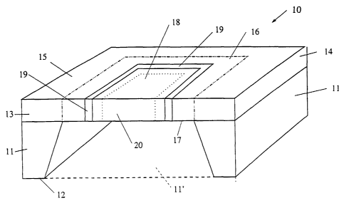
Referring now to Figures 2a and 2b, first and second
examples of a membrane power semiconductor device 10
according to the present invention each have a
semiconductor substrate 11 having a bottom surface 12 that
forms the main bottom surface of the device 10. A first
thin layer 13, which in these examples comprises a
semiconductor layer 14, is formed on the substrate 11 and
has a top surface l5 that forms the main top surface 5 of
the device 10. The original full extent of the substrate
11 is indicated in Figures 2a and 2b by dashed lines.
During manufacture, a portion 11~ of the substrate 11 below
the thin layer 13 is entirely removed up to the thin layer
13 in order to leave a region of the thin layer 13 below
which there is no substrate 11, this region being referred
to herein as a membrane 16 (shown within the dot and dashed
lines). The remaining portions of the substrate 11 form
support legs. The membrane 16 has a bottom surface 17.
The active structure 18 of the power device 10 (indicated
by dotted lines) is in these examples located entirely
within the membrane 16. In the example of Figure 2a, the
active structure 18 is electrically isolated from other
devices or circuits by an isolation layer 19 formed within
CA 02423028 2003-03-20
WO 02/25700 PCT/GBO1/04211
-22-
the membrane 16 between the top surface 15 and the membrane
bottom surface 17 such that the isolation layer 19
surrounds the active structure 18 of the power device 10.
Tn the example of Figure 2b, the isolation layer 19 is
provided outside the membrane 16 within the thin layer 13
such that it surrounds the active structure 18 of the power
device 10. In the examples of both Figure 2a and 2b, the
power device 10 contains a drift layer 20 that is placed in
the semiconductor layer 14 inside the first thin layer 13
and entirely within the membrane 16. The drift layer 20
supports high voltages applied across the main terminals
(not shown) of the power device 10 whilst the power device
10 is off and blocks the voltage across the main terminals.
During such operating mode, the drift layer 20 becomes
partially or ideally completely depleted of mobile
carriers. According to an embodiment of this invention, if
the main terminals are placed on the top surface 15 of the
device and within the membrane 16, the equi-potential lines
in a cross-section of the device along the drift layer 20
are practically perpendicular to both the main top surface
l5 and the membrane bottom surface 17. According to
another embodiment of this invention, if a first main
terminal is placed on the surface 15 and within the
membrane 16 and a second main terminal is placed adjacent
to the bottom membrane and within the membrane 16, the
potential lines are practically parallel to both the top
and bottom surfaces 15,17.
It is preferred that the substrate portion 11~ be
removed as the last or one of the last fabrication steps,
and particularly after formation of all or substantially
all of the structures in and above the thin layer 13 has
been completed, so that the entire substrate 11 can support
CA 02423028 2003-03-20
WO 02/25700 PCT/GBO1/04211
-23-
the whole of the thin layer 13 during these fabrication
steps.
It is worth pointing out here the differences in the
two-dimensional potential distribution of prior art high
voltage devices, such as conventional junction-isolation
(JI) high voltage devices or Silicon-on-Insulator (SOI),
and the membrane power devices according to this invention.
As can be seen in Figures 1a and 1b, for the conventional
devices, the potential lines are virtually perpendicular to
the top surface 5, but as they drop into the body of the
device, they align to be parallel to the bottom substrate
surface 4. Such distribution of the potential lines may
lead to premature breakdown. Figures 3a and 3b show the
two-dimensional distribution of the potential lines in an
example of a simple power device structure according to the
present invention formed by one single high voltage
junction. In the example of Figure 3a, the main terminals
23 are placed on the top surface 15 and the drift region 20
contains for simplicity only one semiconductor layer which
is more lowly doped than the p+ anode region 21 and the n+
cathode region 22. This drift region 20 becomes completely
depleted during the voltage blocking mode and before the
breakdown occurs. Referring to Figure 3a in comparison
with Figure 1a and Figure 1b, it can be seen that the
potential lines are perpendicular or near perpendicular to
both the top surface 15 and the bottom surface 17 of the
membrane 16, and substantially uniformly distributed from
the anode region 21 to the cathode region 22 inside the
drift region 20 such that the value of the breakdown
voltage approaches its ideal limit. In the example of
Figure 3b, the main terminals 23 are on the top surface 15
and bottom surface 17 respectively such that the potential
CA 02423028 2003-03-20
WO 02/25700 PCT/GBO1/04211
-24-
lines are parallel or near parallel to both the top surface
15 and the bottom surface 17, and substantially uniformly
distributed from the anode region 21 to the cathode region
22 inside the drift region 20 such that the breakdown
voltage is ideal for a given thickness of the drift layer
20.
The preferred embodiments of high voltage power
devices according to the present invention also differ from
the prior art devices in the way the isolation is achieved.
The isolation in the preferred membrane power devices is
realised vertically in a perfect manner through the absence
of substrate below the active structure 18 of the membrane
power device 10 and is achieved laterally through the use
of an isolation layer 19 which surrounds the active
structure 18 of the power device 10.
Where provided, the isolation layer 19 may be in the
form of a highly doped semiconductor layer connected to a
matched voltage so that all the junctions associated with
said isolation layer are reverse biased or zero biased. In
this case, the isolation layer acts as an effective
conduction barrier. Figures 4a and 4b each show an example
of a membrane power device 10 having a p+ isolation layer
19 which extends from the top surface 15 to the bottom
membrane surface 17 and which surrounds the active
structure 18. The p+ isolation layer 19 is connected to
ground, which in these examples is assumed to be the lowest
potential available in the power integrated circuit. In
the example of Figure 4a, the isolation layer 19 is
provided within the membrane 16. In the example of Figure
4b, the isolation layer 19 is provided outside the membrane
16.
CA 02423028 2003-03-20
WO 02/25700 PCT/GBO1/04211
-25-
The isolation layer may alternatively be made of an
insulating layer such as silicon oxide and may be in the
form of a trench or LOCOS layer. As a yet further
alternative, the isolation can be made by trenches filled
with a sandwich of oxide and polysilicon layers. Other
insulation materials can also be used. Another alternative
is to use air gaps (so-called "MESA" or "trench"
isolation).
Several isolation layers 19 may be used within the
same membrane 16 to separate plural power devices 10 placed
within the same membrane 16 or to separate bipolar or CMOS
low voltage devices from the power devices 10. Referring
to Figure 5a, there is shown an example of four such power
devices 10 placed within the same membrane 16 and isolated
from each other through isolation layers placed within the
membrane 16. Referring to Figure 5b, there is shown a top
view of an example of four power devices 10 placed on
separate respective membranes 16 and isolated from each
other through isolation layers 19 placed outside the
membranes 16. Referring to Figure 6a, there is shown a
schematic 2D cross-section of a power integrated circuit 40
which contains one membrane power device 10 and CMOS and
bipolar devices 41 placed outside the membrane 16.
Alternatively, the CMOS and bipolar devices 41 can also be
placed on the membrane 16 together with the power devices
10 as shown in Figure 6b or on different membranes 16
formed over the same original substrate 11 as shown in
Figure 6c. The example of Figure 6d differs from the
example of Figure 6c in that the isolation layer 19 is
placed outside the membranes 16. It is evident that the
use of the membranes 16 and isolation layers 19 can provide
CA 02423028 2003-03-20
WO 02/25700 PCT/GBO1/04211
-26-
a very effective electrical isolation between the power
devices 10 and the low power circuits 41 as well as between
adjacent power devices l0.
Referring now to Figure 7, considering that all of the
terminals are placed on the top surface 15 in this example,
a layer 45 that is electrically insulating but which has a
relatively high thermal conductivity may be placed adjacent
the bottom surface 17 of the membrane 16 to help remove a
large fraction of the heat which otherwise may be trapped
inside the membrane 16 while the power device is
operational. In the preferred embodiment, this layer 45 is
formed after the single back-side etching of the
semiconductor substrate 11 is carried out and may be in the
form of a blank deposition of a dielectric material with
high thermal conductivity. Such material may be for
example based on diamond. Other materials, such as boron
nitride, aluminium nitride, and aluminium oxide, can be
used. As shown in Figure 8, the insulating layer 45 may
fill the entire gap in the substrate 11 left by the
membrane formation. In either case, a heat sink 46 may be
in thermal contact with the insulating layer 45 to extract
heat.
As shown in Figures 9a and b, the first thin layer 13
may comprise a thin insulating layer 50, the bottom of
which effectively forms the membrane bottom surface 17, and
at least one semiconductor layer 51 placed on top of the
thin insulating layer 50, as known in for example state-of-
the-art Silicon-on-Insulator (SOI) technology. In this
case, an SOI technology such as bonding wafer, SIMOX or
Unibond may be used in the fabrication of the power
integrated circuits. Alternatively, silicon or diamond can
CA 02423028 2003-03-20
WO 02/25700 PCT/GBO1/04211
-27-
be used. As one of the last steps of the high voltage SOI
process, and as in the examples described above, the
semiconductor substrate 11 below the buried insulating
layer 50 may be partially removed through conventional
patterning by single back-side etching. In this example,
the buried insulating layer 50 acts as an effective etch
stop to form the membrane 16. Importantly, when the main
terminals are placed on the top surface 15 and within the
membrane 16, the buried insulating layer 50 also helps
achieve a uniform distribution of the potential lines
inside the drift layer 20 such that the breakdown voltage
of the membrane power device 10 will be close to its ideal
value. In the example of Figure 9a, the isolation layer 19
is placed within the membrane 16. In the example of Figure
9b, the isolation layer 19 is provided outside the membrane
16.
Again, an insulating layer 45 with relatively high
thermal conductivity may be formed below the membrane 16 as
shown in Figures 10 and 11 to help remove the heat '
laterally to the substrate 11 and/or directly to an
external heat sink 46. In the examples of Figures 10a and
11a, an isolation layer 19 is provided within the membrane
16 whereas in the examples of Figures 10b and 11b, an
isolation layer is provided outside the membrane 16.
In the example shown in Figure 12, a further
electrically insulating layer 55.with enhanced mechanical
properties is placed between the buried insulating layer 50
and the electrically insulating but thermally conductive
layer 45 in the region of the membrane 16 in order to
strengthen the structure of the membrane 16 and help
minimise the risk of mechanical rupture of the membrane 16.
CA 02423028 2003-03-20
WO 02/25700 PCT/GBO1/04211
-28-
This additional insulating layer may also help to
compensate the overall mechanical stress in the membrane 16
and may also enhance the adhesion of the electrically
insulating but thermally conductive layer 45 to the buried
insulating layer 50. It will be appreciated that this
mechanically strong layer 55 can also be placed under the
membrane 16 in any of the other examples described in this
specification that do not have the buried insulating layer
50, such arrangement enhancing the electrical passivation
and/or mechanical performance of the structure including
particularly the resistance to rupture. Several such
mechanically strong insulating layers can be deposited on
the back side of the membrane 16 to increase the thermal
dissipation, passivate electrically and/or consolidate
mechanically the membrane 16 and/or to act as buffer layers
to achieve good adhesion between one layer and another.
The insulating layers 21 and buffer layer may be nitrides,
oxides, amorphous materials or polycrystalline materials.
In the examples shown in Figures 13a to 13c, when the
main device terminals are placed on the top surface 15 and
within the membrane 16, the first thin layer 13 in each
case comprises two semiconductor layers 60,61 of opposite
conductivity type such that the drift region in the power
device 10 is now comprised of two semiconductor regions
60',61' of opposite conductivity type placed above and in
direct contact with each other to form a semiconductor
junction. The presence of these two semiconductor regions
60',61' of different conductivity type and in direct
contact can significantly increase the breakdown voltage of
the device. This is due to the horizontal junction formed
in the vertical direction between the semiconductor layers
60,61 which facilitates the depletion of the entire drift
CA 02423028 2003-03-20
WO 02/25700 PCT/GBO1/04211
-29-
region at much lower voltage than the breakdown voltage.
This means that the drift region acts physically as an
intrinsic layer during the voltage blocking mode and the
potential lines in a vertical cross-section of the device
are perpendicular to the top surface 15 and the membrane
bottom surface 17 and more evenly distributed along the
drift region in the lateral direction. For these
structures, the electric field is therefore practically
uniform along the drift region in the lateral or x
direction. If the electric field reaches its critical
value, avalanche breakdown occurs. As the electric field
at this point is substantially uniform, the breakdown
voltage, which is graphically represented by the area under
the electric field curve in the x direction between the
main terminals of the device, is a maximum. It will be
understood that the doping concentration and the thickness
of the two semiconductor layers 60,61 each play an
important role in obtaining the maximum breakdown voltage
possible and are preferably selected such that the entire
drift region is depleted at relatively low voltage compared
to the rated breakdown voltage. The choice of doping
concentration and thickness of the two semiconductor layers
60,61 is also influenced by the type of power device
employed and by the associated fabrication process.
The example shown in Figure 13b is of the SOI type
having a silicon oxide insulating layer 50. The example of
Figure 13c is again of the SOI type having a silicon. oxide
insulating layer 50 and an electrically insulating but
thermally conductive layer 45 deposited on the back side of
the insulating layer 50. It will be appreciated that an
electrically insulating but thermally conductive layer can
CA 02423028 2003-03-20
WO 02/25700 PCT/GBO1/04211
-30-
also be deposited on the bottom surface 17 of the membrane
16 of the JI example shown in Figure 13a.
In the examples shown in 14a to 14c, which correspond
generally to the examples shown in Figures 13a to 13c, the
drift region in each case is formed by several
semiconductor layers of alternating conductivity type built
on top of each other in the y direction such that the
entire drift region becomes completely depleted at
relatively low voltage compared to the rated breakdown
voltage. Again, it will be appreciated that an
electrically insulating but thermally conductive layer 45
can be deposited on the bottom surface 17 of the membrane
16 of any of these examples.
In the example shown in Figure 15, when again the main
terminals are placed on the top surface 15 within the
membrane 16, the drift region of the membrane power device
l0 comprises plural adjacent layers 70,71,72 of alternating
conductivity type arrayed in the third dimension z. These
adjacent semiconductor regions in the z direction form
transverse semiconductor junctions in the z direction such
that the entire drift region becomes completely depleted at
relatively low voltage compared to the rated breakdown
voltage. The presence of the vertical junction planes in
the z direction on the membrane 16 results in an even
distribution of the potential lines along the drift region
in the x direction, which increases the breakdown voltage
to be close to the ideal value. As in the examples
described above, the potential lines in a vertical (x, y)
cross-section of the device are perpendicular to the top
surface 15 and the membrane bottom surface 17 and are thus
aligned to the y axis. The doping and the thickness of the
CA 02423028 2003-03-20
WO 02/25700 PCT/GBO1/04211
-31-
adjacent semiconductor layers 70,71,72 of different
conductivity type are selected such that the drift region
depletes entirely in the voltage blocking mode at
relatively low voltage compared to the rated breakdown
voltage, thus increasing the breakdown voltage close to its
ideal value. It will be understood that whilst three
semiconductor layers 70,71,72 are shown arrayed in the z
direction, just two or more than three such layers may be
employed. It will further be understood that an
electrically insulating but thermally conductive layer may
be deposited on the bottom surface 17 of the membrane 16 in
order to extract heat from the device 10.
In the example shown in Figure 16, the drift region is
formed by several cells 80 of different conductivity type
placed alternately to each other to form at the top surface
15 and in the x,z plane regular patterns such that again
the entire drift region becomes completely depleted during
the voltage blocking mode so that the potential is
20, distributed uniformly across the drift region. The cells
of different conductivity type may be formed regularly as
shown or irregularly (not shown) in the x,y plane.
In the examples shown in Figures 17a to 17c (which
show respectively a JI device, a SOI device, and a SOI
device having an electrically insulating but thermally
conductive layer 45 applied to the back of the membrane
16), the substrate 11 is removed such that only a part of
the drift region 20 lies within the membrane 16. Thus,
part of the drift region 20 remains outside the membrane 16
(and is therefore positioned above the remaining part of
the substrate 11). The main terminals are placed on the
top surface 15 but, preferably, the high voltage terminal
CA 02423028 2003-03-20
WO 02/25700 PCT/GBO1/04211
-32-
end of the drift region 20 is located within the membrane
16 whilst the low voltage terminal end of the drift region
20 may remain outside the membrane 16. Again, it will be
appreciated that an electrically insulating but thermally
conductive layer 45 can be deposited on the bottom surface
17 of the membrane 16 of any of these examples.
In all of the examples described above and shown in
Figures 2 to 17, the walls of the substrate 12 are angled
to the x,z plane of the lateral device. This is because
the most common technique for back side etching is wet
anisotropic etching, which is typically performed using a
KOH solution. The silicon substrate 11 is a mono-crystal
and the etching rates of anisotropic etchants is dependent
on the crystal orientation. The etch-stop planes are
usually the (111) planes. Those devices of the SOI type
that have the buried oxide layer have the advantage that
the back side etch stops automatically at the buried oxide
since the etch of the oxide is for many etchants (including
KOH) much slower than that of silicon. Alternatively, for
bulk silicon (i.e. non-SOI) devices, the back side etch can
be controlled in time or electrochemically.
Instead of wet anisotropic etching, dry back side
etching may be used for producing any of the membrane power
devices according to the present invention. Dry back side
etching has the advantage that the walls of the substrate
11 are vertical, as shown by way of example in Figures 18
and 18b. This means that the volume occupied by the gap in
the substrate 11 below the membrane 16 is no longer
dependent on the thickness of the substrate 11 and thus a
plurality of membranes 16 with reduced lateral spacing
between them can be achieved in the same chip or integrated
CA 02423028 2003-03-20
WO 02/25700 PCT/GBO1/04211
-33-
circuit more easily. In the example of Figure 18a, the
isolation layer 19 is provided within the membrane 16
whereas in the example of Figure 18b, the isolation layer
19 is provided outside the membrane 16.
In the example shown in Figure 19, the membrane 16 is
formed by front side etching (i.e. surface micro machining)
of the substrate 11. In the example shown, the substrate
11 is only partly removed below the active region 18 of the
device 10 so as to leave°a gap in the substrate 11 below
the active structure 18 which helps to increase the
breakdown capability of the device. Figure 20 is a cross-
sectional view of the example of Figure l9. Figure 21
shows a SOI variant of the example of Figures 19 and 20.
As in all of the examples described above, the presence of
the gap in the substrate 11 below the active region 18
(i.e. the formation of the membrane 16) means that the
potential lines in the drift region 20 are perpendicular to
both the top surface 15 of the device and the bottom
surface 17 of the membrane and are substantially uniformly
distributed inside the drift region 20 such that the
breakdown voltage approaches its ideal limit.
In the examples shown in Figures 22a and 22b, which
are respectively JI and SOI variants, the gap in the
substrate 11 is formed only partially under the drift
region 20 such that only a part of the drift region 20 is
formed in the membrane 16. Again, the main terminals are
placed on the top surface 15 but preferably the high
voltage terminal end of the drift region 20 is placed
within the membrane 16 whilst the low voltage terminal end
may remain outside the membrane 16.
CA 02423028 2003-03-20
WO 02/25700 PCT/GBO1/04211
-34-
Figure 23a shows in detail an example of a membrane
high voltage lateral DMOSFET (LDMOSFET) 10 according to the
present invention in which the drift region 20 is of n
conductivity type, the source region 90 and the drain
region 91 are of n conductivity type and very well doped
with donor impurities to form a good ohmic contact, and the
p well 92 is of p conductivity type. A conventional
insulated gate formed by a thin insulated layer 93 and a
polysilicon and/or metal layer 94 is placed above the p
well 92 and isolated from the source metal layer S by an
insulation layer 95. A thicker insulating layer 96,
referred to as the field oxide, may be present at the top
of the drift layer 20 between the insulated gate and the
drain region. The polysilicon/metal layer 94 may extend by
a short distance above the field oxide 96. In the
on-state, current flows between the drain terminal D which
contacts the n+ drain region 91 and the source terminal
which contacts the n+ source region 90. This current is
controlled by the potential applied to the gate terminal G
which contacts the insulated gate. When a higher potential
is applied to the gate terminal with respect to the source
terminal, a channel of electrons is formed at the surface
of the p well 92 under the insulated gate which allows flow
of electrons from the source region, through the channel,
via the drift region 20 to the drain. The device can be
turned on and off by applying an appropriate potential to
the gate terminal. The high voltage LDMOSFET is placed on
a membrane 16 defined by the top surface 15 and the
membrane bottom surface 17. The membrane bottom surface 17
is situated in the y direction of the cross section between
the top surface 15 and the semiconductor substrate surface
12. The membrane 16 is therefore thin in comparison with
CA 02423028 2003-03-20
WO 02/25700 PCT/GBO1/04211
-35-
the semiconductor substrate 11 such that when the device
operates in the voltage blocking mode, the drift region 20
becomes completely depleted of mobile carriers and the
potential lines are virtually perpendicular to the top
surface 15 and the bottom membrane surface 17 as shown in
Figure 24. This is in contrast with prior art JI LDMOSFETs
in which the drift region is conventionally placed above a
thick semiconductor substrate which in the off-state is not
completely depleted and therefore the potential lines bend
from the initial vertical direction in the drift region to
align with the horizontal direction (x axis) within the
substrate. The advantage of the high voltage membrane
LDMOSFET resides in higher breakdown voltage capacity, a
more uniform distribution of the potential lines at the
surface and a better isolation through the use of a
vertical isolation layer 19 in the membrane 16. In this
example, the isolation layer 19 is made of a highly doped
p+ layer and is connected to the source terminal. It
should be understood that the device shown in Figure 23a
may typically contain several stripes/fingers/cells such
that the device meets the current level and power
specifications. For a 600 V device, the drift region
doping concentration may typically be 1016/cm3, the
thickness of the drift region 20 between 0.2 to 20~m, and
the length of the drift region 30-50~,m. The doping of the
drift region 20 need not be constant and can vary from the
source end to the drain end. For example, at the source
end the doping may be 8x1o15/cm3 while increasing linearly
to 3x10¹⁶/cm3 at the drain end.
Figure 23b shows~an SOI variant of the example of
Figure 23a in which an insulating layer 50 is placed at the
CA 02423028 2003-03-20
WO 02/25700 PCT/GBO1/04211
-36-
bottom of the drift region 20 as part of the membrane 16.
This insulating layer 50 need not be thick as in the case
of prior art SOI high voltage devices but may instead be
very thin since the potential in the voltage blocking mode
(when the device is off) is not supported across it in the
y direction (as in the case of conventional SOI high
voltage devices) but instead along it, in the x direction.
The isolation in this case is made by trench oxides 19 but
other types of isolations, such as p+ layer, may be used.
Figure 23c shows a variation of the example of Figure 23b
in which an electrically insulating layer 45 with a good
thermal conductivity is placed below the membrane to
facilitate the removal of heat to a heat sink 46 and thus
avoid excessive self-heating. In this example, the
isolation layer 19 is provided outside the membrane 16.
Again, it will be appreciated that an electrically
insulating but thermally conductive layer 45 can be
deposited on the bottom surface 17 of the membrane 16 of
any of these examples.
Figures 25a to 25c show in detail examples of Lateral
Insulated Gate Bipolar Transistor (LIGBT) membrane power
devices in which bipolar current conduction within the
drift region 20 suspended on the membrane 16 is employed
and which correspond generally to the LDMOSFETs shown in
Figures 23a to 23c. The main difference between the LIGBT
membrane power devices and the LDMOSFET power devices shown
in Figures 23a to 23c is the use of a highly doped p-type
hole injector layer 100 at the anode. Bipolar conduction
in LIGBT type devices is characterised by conductivity
modulation in the drift layer in order to reduce the on-
state resistance. Again, it will be appreciated that an
CA 02423028 2003-03-20
WO 02/25700 PCT/GBO1/04211
-37-
electrically insulating but thermally conductive layer 45
can be deposited on the bottom surface 17 of the membrane
16 of any of these examples.
Figure 26a is a schematic perspective view of an
example of a membrane device in the form of a power diode.
For a 600 V power diode, the doping concentration of the n
drift region 20 is in the range 3x10¹⁵ to 1o16/cm3 with a
length of 30 to 50~,m. The thickness of the drift layer 20
may be between 0.2~,m to 20~m. The doping of the drift
region 20 need not be constant and can vary from the source
end to the drain end. For example, at the source end the
doping may be 8x10¹⁵/cm3 while increasing linearly to
3x10¹⁶/cm3 at the drain end. For simplicity, only one cell
of the diode is shown. Figure 26b shows schematically an
SOI version of the power diode shown in Figure 26a in which
an insulating layer 50 is formed underneath the drift
region 20 which facilitates a more even distribution of the
potential lines within the drift region 20 and therefore
increases the breakdown ability of the diode. In addition,
the insulating layer 50 acts as a very good etch stop and
hence it makes formation of the membrane 16 easier. To
help remove the heat while the power device is operational,
a highly thermally conductive but electrically insulating
layer 45 (not shown) may again be placed onto the back of
the membrane 16 of the devices shown in Figures 26a and
26b. This layer 45 may be formed by sputtering or other
ways of deposition as one of the last processing steps in
the fabrication of the power integrated circuit as
described above.
CA 02423028 2003-03-20
WO 02/25700 PCT/GBO1/04211
-38-
Figure 27a shows schematically an example of a
membrane power diode which comprises a drift region 20
formed by two layers 100,101 of different conductivity type
n,p arranged vertically one on top of the other. These
layers 100,101 may be formed by epitaxial growth or
preferably by implant of one layer 101 into the other 102.
For a 600 V power diode, the doping concentration of the
two semiconductor layers 101,102 forming the drift region
20 may be between 1016 and 5x10¹⁶/cm3 with a length of 30 to
40 Vim. The thickness of the two semiconductor layers
101,102 is between O.l~.m and 20~,m. If the top
semiconductor layer 101 is formed by implant, then the
doping concentration of the top layer 101 will be higher
than that of the bottom semiconductor layer 102 and hence,
in order to maintain spatial charge equilibrium while the
drift region 20 is depleted, the thickness of the top layer
101 is preferably less than that of the bottom layer 102.
Figure 27b shows schematically an SOI version of the power
diode shown in Figure 27a, whereby an insulating layer 50
is formed underneath the drift region 101,102. An
additional highly thermally conductive but electrically
insulating layer 45 (not shown) may again be placed under
the membrane to facilitate the removal of heat, as
described previously.
Figure 28a shows schematically an example of a 3D
membrane power diode. The drift region of the 3D power
diode is comprised of several pairs of n,p regions 110,111
disposed in the x,z plane such that they form transverse
junctions in the z direction. The widths of these n,p
layers 110,111 may typically be between 0.2~,m and 5~,m,
which represents a small fraction of their typical length.
CA 02423028 2003-03-20
WO 02/25700 PCT/GBO1/04211
-39-
This ensures that the drift region 20 depletes faster in
the z direction than in the x direction and therefore
behaves similarly to an intrinsic layer in the voltage
blocking mode. For a 600V device, the length of the drift
regions 20 (in the x direction) may be approximately 30 ~.m.
The doping of the n,p regions 110,111 may be between
1015/cm3 and 6x10¹⁶/cm3. Preferably, the n,p regions 110, 111
are formed by implanting one layer (e.g. an n layer) 110
into the other layer (e.g. a p layer) 14. Therefore, the
doping concentration of the implanted layer 110 is higher
than that of the background layer 111 and hence to maintain
the charge equilibrium, the width of the implanted layer
110 is preferably smaller than that of the background layer
111. Figure 28b shows schematically a SOI variant of the
example of Figure 28a. Again, in each case, an
electrically insulating but thermally conductive layer 45
(not shown.) may be deposited to extract heat.
Figure 29a shows schematically an example of a single
gate membrane 3D LDMOSFET. The device employs the concept
described above for the 3D membrane power diode to support
a very high voltage between the source and drain terminals
while in the voltage blocking mode, whereas in the
conduction mode the device is similar to a conventional
LDMOSFET and the device of Figure 23a. Figure 29b shows
schematically a SOI variant of the example of Figure 28a.
Again, in each case, an electrically insulating but
thermally conductive layer 45 (not shown) may be deposited
to extract heat.
Figure 30 shows schematically an example of a double
gate membrane 3D LDMOSFET. The device again employs the
concept described above for the 3D membrane power diode to
CA 02423028 2003-03-20
WO 02/25700 PCT/GBO1/04211
-40-
support a very high voltage between the source and drain
terminals. In the conduction mode, the device is
controlled via both the n-channel and p-channel gates such
that unipolar parallel conduction through the n and p
stripes can occur. Bipolar conduction can also take place
by injection of electrons into the p drift layer and of
holes into the n drift layer.
Referring now to Figure 31, another example of a
membrane power semiconductor device 10 according to the
present invention has a semiconductor substrate 11 and a
thin layer 13 which comprises at least one semiconductor
layer 14 and has a top surface 15. The substrate 11 has a
bottom surface 12 that forms the main bottom surface of the
device. During manufacture, a portion of the substrate 11
below the thin layer 13 is removed up to the thin layer 13
to define a membrane 16 with a top surface 15 and a bottom
surface 17. At least one main terminal layer 103 is
attached to the bottom surface 17 and in contact with the
semiconductor layer 14. In a preferred embodiment, said
terminal layer 103 may be in the form of a metal layer
deposited from the back side of the device 10 after the
membrane 16 is formed by single side back-etching. The
metal layer 103 may extend from the membrane bottom surface
17 to the main bottom surface 12 of the device 10 and is
preferably in contact with an external heat sink. The
device comprises at least one further main terminal 104
applied to the top surface 15, in contact with the
semiconductor layer 14 and preferably within the membrane
16, such that in the on-state current conduction between
the main top terminal 104 and the main bottom terminal 103
is substantially vertical and perpendicular to the top
surface 15 and the membrane bottom surface 17. The device
CA 02423028 2003-03-20
WO 02/25700 PCT/GBO1/04211
-41-
may have a control terminal 105 placed on the surface 15 to
control the current between the main terminals 103,104.
The power device l0 contains a drift layer 20 placed inside
the first thin layer 13, within the semiconductor layer 14.
At least a portion of the drift layer 20 is placed within
the membrane 16.
The drift layer 20 supports the high voltages applied
across the main terminals 103,104 whilst the power device
10 is off and blocks the voltage across the main terminals
103 and 104. During such operating mode, the drift layer
becomes partially or completely depleted of mobile
carriers and the equipotential lines in a cross-section of
the device 10 are parallel with the top surface 15 and the
15 membrane bottom surface 17 and substantially uniformly
distributed between the top end of the drift layer 20 and
the bottom end of the drift layer 20.
The removal of the substrate 11 under part of the thin
20 layer 13 results in a better trade-off between the on-state
resistance and the breakdown performance. The uniform
distribution of the potential lines inside the drift region
in the membrane 16 results in ideal breakdown voltage for a
given thickness of the drift region 20. Because the
substrate 11 is removed under part of the thin layer 13,
there is no substrate parasitic electrical and thermal
resistance and isolation (not shown) from other devices and
circuits present in the chip is easier to make. The
terminal layer 103 is preferably highly thermally
conductive to help dissipation of heat from the membrane
region 11 to an external heat sink (not shown).
CA 02423028 2003-03-20
WO 02/25700 PCT/GBO1/04211
-42-
Figure 32 shows schematically an example of a
membrane power device l0 according to the present invention
in which dry back-side etching is used to produce the
membrane 16. The walls of the remaining portions of the
substrate 11 are vertical as shown in Figure 32. Following
the membrane formation by dry etching, a terminal layer 103
is applied to the membrane bottom surface 17 to form one of
the main terminals of the device 10. As previously
explained the dry etch has the advantage that the volume
occupied by the gap in the substrate 11 is no longer
dependent on the thickness of the substrate 11 and
therefore the area of the membrane 16 is easier to control.
Figure 33 shows a cross-section of the device 10 shown
in Figure 31. In this example, a termination region 106 of
the device 10 is placed outside the membrane 16 whilst the
active region 18 is placed within the membrane 16. The
termination region 106 is used in power devices to suppress
premature breakdown at the edge of the device 10 while the
device blocks the voltage between the main terminals. The
termination region 106 does not play an active role in the
on-state and hence substantially no current conduction
takes.place in the termination region 106 during on-state
operation. To minimise the on-state resistance and power
losses, it is desirable that the drift layer 20 is as thin
as possible. However, to support a higher breakdown at the
device edge and thus force actual breakdown to occur in the
active region, the termination region 106 is preferred to
be thicker. For this reason, the active region 18 is
placed inside the membrane 16 region whilst preferably the
termination region 106 lies outside the membrane 16 on a
thicker layer than the membrane 16. The termination 106 in
this example benefits from having a substrate 11 underneath
CA 02423028 2003-03-20
WO 02/25700 PCT/GBO1/04211
-43-
which facilitates the spreading of the depletion region in
a wider volume while the device 10 blocks the high voltage
across the main terminals. The termination region 106 and
the substrate 11 may have a different doping than the drift
layer 20 placed within the active region 18. In a
preferred embodiment, the substrate 11 is more lowly doped
than the drift region 20. The termination region 106 can
be in the form of highly doped floating rings (known per
se) encircling the active region 18 of the device 10 which
help to spread the depletion region on a larger area at the
surface, each pair of rings withstanding in the .space
between them a fraction of the total voltage, thereby
reducing the risk of edge premature breakdown. This
termination, known as floating ring termination, may
comprise field plates and channel/depletion stoppers.
Alternatively, the termination may be in the known form of
junction termination extension (JTE) or field plate
termination.
Figure 34 shows in detail an example of a membrane
vertical power MOSFET according to the present invention in
which the active region 18 contains a drift region 20 of n
conductivity type placed within the membrane 16 with a
termination region 106 placed outside the membrane region
16. In this example, the termination region 106 is made of
several concentric floating highly doped p-type rings 107
and a final highly doped n-type depletion stopper ring 108.
The power MOSFET has highly doped n-type source 109 and
drain 122 regions, an insulated gate formed by an
insulating layer 121 and a polysilicon/metal layer 105
which acts as a control terminal. The source terminal 104
is placed on the top surface 15 and the drain terminal 103
is attached to the membrane bottom surface 17. The source
CA 02423028 2003-03-20
WO 02/25700 PCT/GBO1/04211
-44-
terminal 104 contacts both the source region 109 and the p
well 120. The drain terminal 103 contacts the highly doped
n-type drain region 122. The operation of the MOSFET in
the on-state relies on the formation of an inversion layer
at the surface of the p well 120 when a gate voltage is
applied to the control terminal 105. In this mode,
electrons are transported from the source region 109 via
the said inversion layer formed in the p well 120 through
the drift region 20 to the drain region 122. To minimise
the on-state resistance, it is preferred that the drift
region 20 is thin and relatively more highly doped compared
to the substrate 11. During the off-state, when a high
voltage is applied across the main terminals 103,104, the
drift region 20 is completely depleted of mobile carriers
and supports the largest fraction of the voltage in the
active area. The potential lines in the drift region 20
are parallel to the top surface 15 and the membrane bottom
surface 17 and ideally uniformly distributed inside the
drift layer 20. In the termination region 106, the
depletion region has more room to spread inside the
substrate 11, thereby avoiding crowding of potential lines
and premature breakdown at the edge of the drift region.
The substrate 11 may be more lowly doped than the surface
of the termination region 106 and the drift region 20. It
should be noted that there is substantially no on-state
current conduction in the termination region 106 and
therefore the thick and relatively lowly doped substrate 11
does not affect adversely the on-state resistance and does
not add additional power losses as would have been
otherwise expected if the substrate 11 had been present
under the membrane 16. It will be understood that for
simplicity, the internal structure of the MOSFET is only
shown in two dimensions in Figure 34.
CA 02423028 2003-03-20
WO 02/25700 PCT/GBO1/04211
-45-
Figure 35 shows a schematic perspective view of a 3D
membrane power device l0 with a terminal 103 placed on the
bottom 17 of the membrane 16. The drift region of the 3D
membrane power device is comprised of several pairs of n, p
regions 110,111 disposed in the x,z plane such that they
form transverse.junctions in the z direction. If the
regions 110,111 are thinner in the z direction than in the
y direction, the drift region 20 depletes faster in the z
direction than in the y direction when a high voltage is
applied across the main bottom terminal 103 and a top main
terminal (not shown) placed on the top surface 15. This
ensures higher breakdown ability and that the potential
lines are parallel to the top surface 15 and the bottom
surface 17 and substantially uniformly distributed across
the drift region.
Figures 36a to 36c show schematically an example of a
method of fabricating a device 10 according to the present
invention. In this example, the thin layer 13 comprises a
semiconductor layer 14 under which is provided a buried
insulating oxide layer 50 under which is provided the
substrate 11. As in the examples described above (for
example with reference to Figure 9), the semiconductor
substrate 11 below the buried insulating layer 50 is
partially removed by back-side etching with°the buried
insulating layer 50 acting as an etch-stop to form the
membrane 16, as shown in Figure 36a. In this example, as
indicated in Figure 36b, the portion of the buried
insulating layer '50 below the membrane portion of the
semiconductor layer 14 is also then removed so that the
exposed bottom surface of the semiconductor layer 14
provides the bottom surface 17 of the membrane 16. This
CA 02423028 2003-03-20
WO 02/25700 PCT/GBO1/04211
-46-
removal of the buried insulating layer 50 in the region of
the membrane 16 allows a terminal layer 103 to be deposited
on the back-side of the device. As shown, in this example,
the bottom terminal layer 103 extends over the whole of the
bottom surface 17 of the membrane 16 and down the inwardly
facing sidewalls and under the bottom surfaces of the
remaining leg portions of the substrate 11.
Figures 37 to 40 show schematically examples of a
membrane power device 10 with a terminal attached to the
membrane bottom surface in an integrated circuit containing
low voltage/low power devices and circuits and other power
devices.
Figure 37 shows for example four membrane power
devices each featuring independent terminals with four main
terminals 103 attached to the bottom of the membrane, and
four main terminals 104 placed on the top of the membrane.
Independent control terminals 105 can be used to control
the operation of each individual power device. The power
devices placed on the membrane 16 are isolated from each
other through isolation layers 19 as described in previous
examples.
Figure 38a shows a schematic cross-section of a power
integrated circuit 40 which contains one membrane power
device 10 with a main terminal 103 applied to the bottom
surface and low power CMOS and bipolar devices 41 placed
outside the membrane 16. Alternatively, the CMOS and
bipolar devices 41 can also be placed within the membrane
16 as shown in Figure 38b or on a separate membrane 16
formed over the same original substrate 11 as shown in
Figure 38c. Preferably the bottom terminal 103 does not
extend under the low power devices and circuits. The
CA 02423028 2003-03-20
WO 02/25700 PCT/GBO1/04211
-47-
example of Figure 38d differs from that of Figure 38c in
that the isolation layers 19 are placed outside the
membranes 16.
The structures shown schematically in Figures 39a to
39d are SOI corespondents to those shown in Figures 38a to
38d. In these examples, the insulating layer 50 is used as
an etch stop to farm the membrane 16. The insulating layer
50 also helps to isolate individual devices placed within
the thin layer 13 from the substrate 11.
Figures 40a to 40d show schematically possible ways to
integrate more than one membrane power device with
independent main bottom terminals 103 in the same power
integrated circuit 40. In the example of Figure 40a, two
power devices 10a and 10b each having a respective bottom
main terminal 103a,103b are integrated on the same membrane
16. In the example of Figure 40b, an insulating layer 50
is used to form the membrane 16 and help isolation of
individual devices within the power integrated circuit 40.
The example of Figure 40c differs from that of Figure 40b
in that the outer isolation layers 19 are placed outside
the membrane 16. The inner isolation layer 19 in the
example of Figure 40c which separates the first power
device 10a from the second power device 10b remains within
the membrane 16 as also shown in the example of Figure 40b.
In the example of Figure 40d, the membrane power devices
10a,10b having independent bottom terminals 103a,103b
respectively are placed on different membranes 16a,16b
respectively formed above the same original substrate 11.
To isolate the membrane power devices from each other, a
further membrane 16c which may contain one isolation layer
CA 02423028 2003-03-20
WO 02/25700 PCT/GBO1/04211
-48-
19 is formed above the original substrate 11 and placed
between the adjacent membrane power devices 10a,10b.
Figures 41a to 41c show in more detail examples of a
membrane vertical power MOSFET. Figure 41a shows a
membrane vertical power MOSFET according to an embodiment
of the present invention using the known DMOS technology.
The power MOSFET has highly doped n-type source 109 and
drain 122 regions, an insulated gate formed by an
insulating layer 121 and a polysilicon/metal layer 105
which acts as a control terminal. The source terminal 104
is placed on the top surface 15 and the drain terminal 103
is attached to the membrane bottom surface 17. The source
terminal 104 contacts both the source region 109 and the p
well 120. The drain terminal 103 contacts the highly doped
n-type drain region 122. The operation of the MOSFET in
the on-state relies on the formation of an inversion layer
at the surface of the p well 120 when a gate voltage is
applied on the control terminal 105. In this mode,
electrons are transported from the source region 109 via
the said inversion layer formed in the p well 120 through
the drift region 20 to the drain region 122. During the
off-state, when a high voltage is applied across the main
terminals 103,104, the drift region 20 is completely
depleted of mobile carriers and supports the largest
fraction of the voltage in the active area. The potential
lines in the drift region 20 are parallel to the top
surface 16 and the membrane bottom surface 17 and ideally
uniformly distributed inside the drift layer 20. The
highly doped n-type drain layer 122 may be a buried layer
formed prior to the back-side etch which defines the
membrane 16. In this way, the n-type layer 122 may be used
as an indirect means to stop the back-etch using a known
CA 02423028 2003-03-20
WO 02/25700 PCT/GBO1/04211
-49-
electrochemical technique. To facilitate the
electrochemical etch, the substrate 11 may be of p-type
doping to form a junction with the said n-type layer 122.
The example of Figure 41b differs from the example of
Figure 41a in that the highly doped n-type drain layer 122
is formed by masked or blank back-side deposition after the
membrane 16 is formed. The drain terminal 103 is applied
to the membrane bottom surface 17 after the membrane 16 is
formed and the n-type drain layer 122 is introduced in the
membrane 16 from the back-side of the device.
Figure 41c shows an example of a membrane vertical
power MOSFET according to an embodiment of the present
invention using trench technology. The structure in Figure
41c differs from that shown in Figure 41b in the way the
insulated gate is formed at the top of the structure. In
the structure of Figure 41c, the inversion layer in the 120
is formed vertically, substantially perpendicular to the
top surface 15. This structure has the advantage of
enhanced channel density and higher packing density.
Figures 42a to 42c show in detail examples of vertical
Insulated Gate Bipolar Transistors (IGBT) membrane power
devices in which bipolar conduction within the drift region
20 suspended on the membrane 16 is employed and which
generally correspond to the membrane vertical power MOSFETs
shown in Figures 41a to 41c. The main difference in the
IGBTs is the use of a highly doped p-type hole injector
anode layer 123 in contact with the anode terminal 103.
Bipolar conduction of the current is substantially
perpendicular to the top surface 15 and is characterised by
conductivity modulation in the drift layer 20 to reduce the
on-state voltage drop across the drift layer 20. The
CA 02423028 2003-03-20
WO 02/25700 PCT/GBO1/04211
-50-
n-type buffer layer 122 and the p-type anode layer 123 may
be formed prior to the formation of the membrane 16 as
shown in Figure 42a or after the formation of the membrane
16 as shown in Figure 42b. Figure 42c shows a trench
variant of the membrane IGBT shown in Figure 42b. In
Figure 42a, the anode layer 123 may be used directly or
indirectly as an etch-stop to form the membrane 16.
Figure 43a and b show examples of a power integrated
circuit containing two vertical power MOSFETs lOa,lOb using
trench technology and suspended on separate membranes
16a,16b. In the example of Figure 43a, the devices 10a,10b
feature independent terminals and are isolated from each
other through the use of a third membrane 16c and an
isolation layer 19. The three membranes 16a,16b,16c are
formed in the same step and in this example by use of a
back-side dry etch which results in vertical walls for the
remaining leg portions of the substrate 11 which, as
previously described, are advantageous for obtaining a
better control of the membrane area and integrating a large
number of devices within the same chip. The example of
Figure 43b is a SOI variant of the example of Figure 43a.
The isolation layer 19 in this case is placed outside the
membranes 16a and 16b and together with the buried
dielectric layer 50 ensures an effective isolation of the
two power devices 10a,10b from each other. The examples in
Figures 43a and 43b show two membrane power MOSFETs
integrated in the same chip, but any other membrane power
devices can be used in a similar way and isolated from each
other as shown in this figure.
Although the above examples refer primarily to
silicon, the power membrane devices of the present
CA 02423028 2003-03-20
WO 02/25700 PCT/GBO1/04211
-51-
invention can be built on other semiconductors, such as for
example silicon carbide (SiC), diamond, GaAs, GaN or other
III-V materials.
The drift region as part of the first thin layer 13
can be made of wide band gap materials, such as diamond,
GaAs, GaN and SiC or can be made of heterojunctions such as
GaN and AlGaN combinations or other suitable materials.
The insulating layer 50 is described primarily with
reference to silicon dioxide but other insulating or semi-
insulating materials, such as diamond, nitride or
combinations of nitride and oxide, can be used.
The heat sink layer 45 can be made of diamond,
aluminium nitride, boron nitride or other materials with
good electrically insulating properties and high thermal
conductivity.
Some examples of the thickness of the membrane 16 have
already been given above. Generally, in a lateral device,
the membrane 16 may have a thickness in the range 0.1~,m to
10~m or 20~,m or so. Generally, in a vertical device, the
membrane 16 may have a thickness in the range 6~,m or 10~,m
to 60~m or 100~m or 180~,m or so.
Embodiments of the present invention have been
described with particular reference to the examples
illustrated. However, it will be appreciated that
variations and modifications may be made to the examples
described within the scope of the present invention.