Note: Descriptions are shown in the official language in which they were submitted.
CA 02423225 2003-03-20
WO 02/31576 PCT/USO1/32092
LIGHT ADJUSTABLE ABERRATION CONJUGATOR
CROSS REFERENCE TO RELATED APPLICATIONS
(0001] This application is based on United States Application
Serial No. 60/239,349, filed October 11, 2000.
BACKGROUND OF THE INVENTION
Field of the Invention
(0002] This invention relates to methods of correcting for
aberrations in an optical system, more specifically through the use and
placement of media at appropriate positions in an optical system, the
properties of the media being such that the refraction of the media can be
modified by exposure of the media to light.
Background Information
(0003] Adaptive optical systems have been employed by
astronomers, optical engineers, and vision scientists to compensate for
wavefronfi aberrations generated by the atmosphere, telescope optics, optical
design errors, and the inherent wavefront errors of the human visual system.
In these systems, a wavefront sensor is used to measure the aberrations from
the target to the imaging sensor. A computer is used to calculate the
conjugate to the measured aberrations and deform a mirror with actuators to
place the conjugate aberration on the deformable mirror's surface. The
deformable mirror (DM) is usually placed at the image of the pupil to minimize
isoplanatic errors in the optical system. When the DM is not placed at the
pupil or an image of the pupil, the angular field of view, which the
aberrations
are corrected over, will not be as large.
(0004] To correct optical system aberrations, opticians will polish
compensating surfaces on one of the elements. As an example, conjugate
errors are often polished into the secondary mirror of a two-mirror telescope
to
compensate for errors in the primary mirror. This process can take hours in a
production shop and days in a precision optical fabrication facility. As
another
example, the spherical aberrations present in typical camera systems are
CA 02423225 2003-03-20
WO 02/31576 PCT/USO1/32092
removed by polishing an aspheric surface onto one of the lens surfaces.
Thus, fabricating an aberration conjugator as such is known and has been
used in a number of applications.
[0005] In addition to adaptive optics and optical polishing, other
approaches address the correction of aberrations in optical systems. These
include ion polishing, the deposition of thin films, the use of binary optics,
holographic elements, real time holography, and spatial light modulators.
[0006] All of these approaches have drawbacks. For example
ion polishing and thin film deposition must be performed in a vacuum.
Virtually all of these methods are costly and time consuming. Some are
disadvantageous because of low efficiencies or because polarized light must
be used. A less labor intensive, cost effective, and faster method of
correcting aberrations in optical systems would provide significant
advantages.
SUMMARY OF THE INVENTION
[0007] The present invention is a method of correcting
aberrations in an optical system, and the correction structure that results
from
fihe method. More particularly, aberrations in an optical system are corrected
by applying a light adjustable aberration conjugator layer to a component of
the system, measuring the type and magnitude of the aberrations, applying
radiation to the conjugator layer to change the refraction of the conjugator
layer to compensate for the aberration, and locking in the desired optical
property. The light adjustable media comprises a refraction modulating
composition (RMC) dispersed in a polymer matrix. Optical and optical system
aberrations arise from fabrication, alignment , and residual design errors.
The
aberration information in the optical system is measured to determine the
exposure profile needed to convert a layer of the media placed in the
appropriate part of the optical system into a form which will be the conjugate
of the aberration and therefore null the aberration. Thus, the method of the
invention, and the structure created thereby, will correct fixed aberrations
in
an optical system by putting the conjugate aberrations of the optical system
on one of the surfaces in the optical system.
2
CA 02423225 2003-03-20
WO 02/31576 PCT/USO1/32092
[0008] The foregoing has outlined rather broadly the features
and technical advantages of the present invention in order that the detailed
description of the invention that follows may be better understood. The
foregoing and additional features and advantages of the invention that will be
described hereinafter form the subject of the claims of the invention. It
should
be appreciated by those skilled in the art that the conception and specific
embodiment disclosed might be readily utilized as a basis for modifying or
designing other structures for carrying out the same purposes of the present
invention. It should also be realized by those skilled in the art that such
equivalent constructions do not depart from the spirit and scope of the
invention as set forth in the appended claims. The novel features which are
believed to be characteristic of the invention, both as to its organization
and
method of operation, together with further objects and advantages will be
better understood from the following description when considered in
connection with the accompanying Figures. It is to be expressly understood,
however, that each of the Figures is provided for the purpose of illustration
and description only and is not intended as a definition of the limits of the
present invention.
BRIEF DESCRIPTION OF THE DRAWINGS
The invention herein will be better understood by reference to the
attached figures, in which:
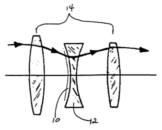
[0009] Figure 1 shows a light adjustable aberration conjugator
layer applied to the surface of a center negative element in a double Gauss
lens;
[0010] Figure 2a shows a light adjustable aberration conjugator
layer applied to the secondary mirror of a telescope, for reflection from the
layer;
(0011] Figure 2b shows a light adjustable aberration conjugator
layer applied to the secondary mirror of a telescope, for transmission through
the layer for reflection from the mirror;
3
CA 02423225 2003-03-20
WO 02/31576 PCT/USO1/32092
[0012] Figure 3a shows a light adjustable aberration conjugator
layer applied to either the forward or rearward surface of a window at the
exit
pupil of a telescope having a particular construction;
[0013] Figure 3b shows a light adjustable aberration conjugator
layer applied to either the rearward surface of a window at the exit pupil of
a
telescope of another construction;
[0014] Figure 4 shows an exposed light adjustable aberration
conjugator layer on a flat substrate; and
[0015] Figure 5 shows a light adjustable aberration conjugator
layer that is protected between two planes, window type substrates.
DESCRIPTION OF REPRESENTATIVE EMBODIMENTS
[0016] The purpose of this invention is to more easily correct the
fixed aberrations in an optical system by placing the conjugate of the optical
system aberrations on one of the surfaces in the optical system. Fixed,
optical system aberrations include aberrations from fabrication , alignment ,
and residual design errors. Correcting the fixed aberrations with light rather
than by polishing or by the use of deformable mirrors saves time and money.
The invention has advantages over ion polishing, surface layered optical
coatings and deposited masks, which have to be performed in a vacuum and
the surface being modified must be on an outer surface. The invention also
has advantages over surface buildup with optical coatings and masks
because they also have to be applied in a vacuum chamber and to an outer
surface. The light adjustable material described herein can be applied to any
surface in the optical train, as long as the optical system transmits enough
of
the light at the irradiation wavelength to cause polymerization of the
dispersed
refractive modulating composition (RMC). The method of the invention need
not be performed in a vacuum.
[0017] The media used in the invention to correct optical system
aberrations is a light sensitive material. In particular, the material
comprises
a first polymer matrix and a refraction modulating composition (RMC)
4
CA 02423225 2003-03-20
WO 02/31576 PCT/USO1/32092
dispersed therein, which will be described in greater detail hereinafter. When
it is exposed as described herein, in the appropriate manner, the refraction
of
the material changes to compensate for aberrations in the optical system. It
is
referred to herein as a light adjustable aberration conjugator. The starting
material can be applied, in a preferred embodiment, in a thin layer,
approximately 1 mm thick, to almost any surface in the optical system,
preferably.to one of the smaller surfaces.
(0018] Figure 1 shows a lighfi adjustable aberration conjugator
layer 10 applied to an interior lens surface, specifically, to the surFace of
center negative element 12 in a double Gauss lens 14.
(0019] Figures 2a shows a light adjusfiable aberration conjugator
layer 16 applied to the secondary mirror 18 of a telescope 20 for reflection
from the layer 16. In this case the layer is coated with a reflective coating
after irradiating with the profiling beam and the locking beam. Figure 2b
shows a light adjustable aberration conjugator-transmitting layer 22 placed
over a mirror surFace 24 of a telescope 26 and used in a double pass. This is
referred to as a catadioptric design and corrects for fabrication errors but
not
for alignment errors after re-installing the secondary mirror.
(0020] Figure 3a shows a light adjustable aberration conjugator
layer 28 or 28a applied to a window 30 at the exit pupil of a telescope 32 of
a
particular construction, on either the front surface of the forward lens 34 or
the
rear surface of the rearward lens 36. Figure 3b shows a light adjustable
aberration conjugator layer 38 applied to the rear surface of the rearward
lens
40 at the exit pupil of a telescope 42 of another construction. The telescopes
can have a small refractive design or a larger reflective design. Since the
aberration conjugator layer is on the outside of the optical system, at a
pupil
plane, and on a non-power element, it is the easiest to implement and can be
added at any time after the optical system is fabricated. The advantages are
much greater if the telescope is a large two-mirror reflective telescope. All
optical systems will have some amount of fabrication errors. The tolerance on
these errors will depend on its application and the cost will depend on the
tolerances specified by the user.
CA 02423225 2003-03-20
WO 02/31576 PCT/USO1/32092
(0021] The light adjustable aberration conjugator layer 44 can be
placed on a flat substrate 46 and be exposed as shown in Figure 4 (or as
shown in Figure 3), or it can be protected by another lens in the system (as
shown with a curved surface in Figure 1. Another technique is to place the
light adjustable aberration conjugator layer between two optical substrates. A
void 48 between the light adjustable aberration conjugator layer 50, shown in
Figure 5, and opposing protecting windows 52 and 54 (which could,
alfiernatively, be lenses) can be a vacuum or it can be filled with a gas,
liquid
or solid. An example of a suitable solid is another polymer that is
polymerized
after pouring over the light adjustable aberration conjugator. It would have
to
have a different refractive index to be effective, unless the refractive index
modulation alone provides sufFicient aberration correction. There are several
advantages of using a liquid or solid over the light adjustable aberration
conjugator layer, i.e., the light adjustable aberrafiion conjugator layer is
better
protected and the layer does not have to be as precise. The disadvantage is
that the dynamic range of correction will be less.
(0022] One embodiment of this invention is to use a wavefront
sensor such as an interferometer or Shack-Hartmann sensor to measure the
optical system aberrations and input them into a computer program that
contains a light adjustable aberration conjugator nomogram. The computer
calculates the required irradiation pattern. An irradiation system, operating
at
the appropriate wavelength irradiates the light adjustable aberration
conjugator material with the calculated pattern. A special setup may be
required if the light adjustable aberration conjugator layer is placed on the
internal surface of the lens system. A more detailed description of the use of
a Shack-Hartmann sensor, and a description of sources for radiation that can
be used to expose/irradiate the material to form the light adjustable
aberration
conjugator, are given hereinafter under the heading "Exposing a Light
Adjustable Aberration Conjugator Layer"
(0023] The complete process can be automated for production
lines of lenses or mirror telescopes. The process can also be provided as a
service if the customer sent in the measured aberrations and the pupil size or
6
CA 02423225 2003-03-20
WO 02/31576 PCT/USO1/32092
size of the light adjustable aberration conjugator surface. It can also be a
post
production process if the light adjustable aberration conjugator was placed on
an exterior surface or an accessible surface. The invention can improve the
optical performance of many different types of optical systems at an
affordable cost and schedule. Once the aberrations are obtained and the
setup is complete, the calculations and irradiation time should take less than
2
minutes and the diffusion time should take between 3 to 24 hours. This
process reduces the labor, money, and time intensive processes of optical
polishing, ion polishing, and thin film deposition. This invention will allow
manufactures to correct camera lenses on the assembly line, researchers to
correct optics on an optical bench, astronomers to correct fixed errors on
large telescopes, and allow manufactures to design less expensive lens
systems by incorporating low cost corrector plates.
[0024] In a specific embodiment of the invention, the optical
element that becomes the light adjustable aberration conjugator comprises a
first polymer matrix and a refraction modulating composition (RMC) dispersed
therein. Such a composition is described in detail in International
Application
Serial No. PCT/US99/41650, filed on October 13, 1999 and published July 20,
2000, the disclosure of which is incorporated herein by this reference. As
disclosed in that application, the first polymer matrix forms the optical
element
framework and is generally responsible for many of its material and optical
properties. The RMC may be a single compound or a combination of
compounds that is capable of stimulus-induced polymerization, preferably
photo-polymerization. As used herein, the term "polymerization" refers to a
reaction wherein at least one of the components of the RMC reacts to form at
least one covalent or physical bond with either a like component or with a
different component. The identities of the first polymer matrix and the RMCs
will depend on the end use of the optical element. However, as a general
rule, the first polymer matrix and the RMC are selected such that the
components that comprise the RMC are capable of diffusion within the first
polymer matrix. Put another way, a loose first polymer matrix will tend to be
paired with larger RMC components and a tight first polymer matrix will tend
to be paired with smaller refraction modulating composition components.
7
CA 02423225 2003-03-20
WO 02/31576 PCT/USO1/32092
[0025] Upon exposure to an appropriate energy source (e.g.,
heat or light), the RMC typically forms a second polymer matrix in the
exposed region of the optical element. Light sources that may be used are
also described in International Application Serial No. PCT/US99/41650. The
presence of the second polymer matrix changes the material characteristics of
this portion of the optical element to modulate its refraction capabilities.
In
general, the formation of the second polymer matrix typically changes the
radius of curvature (i.e. the exposed area swells), increases the refractive
index, or both, of the affected portion of the optical element.
[0026] After exposure, the RMC in the unexposed region will
migrate into the exposed region over time. The amount of RMC migration into
the exposed region is dependent upon the intensity, wavelength, spatial
profile, and duration of the applied light as well as the physical and
chemical
properties of the polymer composition. All of these factors may be precisely
controlled to achieve the desired result. If enough time is permitted, the RMC
components will re-equilibrate and redistribute throughout the optical element
(i.e., the first polymer matrix, including the exposed region). When the
region
is re-exposed to the energy source, the RMC that has since migrated into the
region (which may be less than if the refraction modulating composition were
allowed to re-equilibrate) polymerizes to further increase the formation of
the
second polymer matrix. This process (exposure followed by an appropriate
time interval to allow for diffusion) may be repeated until the exposed region
of the optical element has developed the desired optical properties. At this
point, the entire optical element is exposed to the energy source to "lock-in"
the desired optical properties by evenly polymerizing the remaining RMC
components in the optical element. Evenly polymerizing any remaining RMC
components will remove the driving force for diffusion (i.e. prevent any
further
change in refraction) and prohibit any change in the optical properties of the
aberration conjugation layer by subsequent exposure of the optical element to
an appropriate energy source.
[0027] The first polymer matrix is a covalentiy or physically
linked structure that functions as structure matrix for the aberration
conjugator
CA 02423225 2003-03-20
WO 02/31576 PCT/USO1/32092
material and is formed from a first pre-polymer matrix composition. In
general, the first polymer matrix composition comprises one or more
monomers that upon polymerization will form the first polymer matrix. The
first polymer matrix composition optionally may include any number of
formulation auxiliaries that modulate and improve any property of the optical
element. Illustrative examples of suitable first pre-polymer matrix
composition
monomers include acrylics, methacrylates, phosphazenes, siloxanes, vinyls,
homopolymers and copolymers thereof. As used herein, a "monomer" refers
to any unit (which may itself either be a homopolymer or copolymer), which
may be linked together to form a polymer containing repeating units of the
same. If the first pre-polymer matrix composition monomer is a copolymer, it
may be comprised of the same type of monomers (e.g., two different
siloxanes) or it may be comprised of different types of monomers (e.g., a
siloxane and an acrylic).
[00281 In one embodiment, the one or more monomers that form
the first polymer matrix are polymerized and cross-linked in the presence of
the RMC. In another embodiment, polymeric starting material that forms the
first polymer matrix is cross-linked in the presence of the RMC. Under either
scenario, the RMC components must be compatible with and not appreciably
interfere with the formation of the first polymer matrix. Similarly, the
formation
of the second polymer matrix should also be compatible with the exisfiing
first
polymer matrix. Put another way, the first polymer matrix and the second
polymer matrix should not phase separate and light transmission by the
optical element should be unaffected.
[0029] As described previously, the RMC may be a single
component or multiple components so long as: (i) it is compatible with the
formation of the first polymer matrix; (ii) it remains capable of stimulus-
induced polymerization after the formation of the first polymer matrix; and
(iii)
it is freely diffusable within the first polymer matrix. In one embodiment,
the
stimulus-induced polymerization is photo-induced polymerization.
[0030] Illustrative examples of a suitable first polymer matrix
include: poly-acry(ates such as poly-alkyl acrylates and poly-hydroxyalkyl
9
CA 02423225 2003-03-20
WO 02/31576 PCT/USO1/32092
acrylates; poly-methacrylates such as poly-methyl methacrylate ("PMMA"),
poly-hydroxyethyl methacrylate ("PHEMA"), and poly-hydroxypropyl
methacrylate ("HPMA"); poly-vinyls such as poly-styrene and poly-
vinylpyrrolidone ("PNVP"); poly-siloxanes such as poly-dimethylsiloxane; poly-
phosphazenes, and copolymers of thereof. U.S. Patent No. 4,260,725 and
patents and references cited therein (which are all incorporated herein by
reference) provide more specific examples of suitable polymers that may be
used to form the first polymer matrix.
[0031] In preferred embodiments, the first polymer matrix
generally possesses a relatively low glass transition fiemperature (Tg) such
that the resulting optical element tends to exhibit fluid-like and/or
elastomeric
behavior, and is typically formed by crosslinking one or more polymeric
starting materials wherein each polymeric starting material includes at least
one crosslinkable group. Illustrative examples of suitable crosslinkable
groups include but are not limited to hydride, acetoxy, alkoxy, amino,
anhydride, aryloxy, carboxy, enoxy, epoxy, halide, isocyano, olefinic, and
oxime. In more preferred embodiments, each polymeric starting material
includes terminal monomers (also referred to as endcaps) that are either the
same or different from the one or more monomers that comprise the
polymeric starting materials but include at least one crosslinkable group. In
other words, the terminal monomers begin and end the polymeric starting
material and include at least one crosslinkable group as part of its
structure.
Although it is not necessary for the practice of the present invention, the
mechanism for crosslinking the polymeric starting material preferably is
different than the mechanism for the stimulus-induced polymerization of the
components that comprise the RMC. For example, if the RMC is polymerized
by photo-induced polymerization, then it is preferred that the polymeric
starting materials have crosslinkable groups that are polymerized by any
mechanism other than photo-induced polymerization.
[0032] In some embodiments there may be used a class of
polymeric starting materials for the formation of the first polymer matrix
comprising poly-siloxanes (also known as "silicones") endcapped with a
CA 02423225 2003-03-20
WO 02/31576 PCT/USO1/32092
terminal monomer which includes a crosslinkable group selected from the
group consisting of acetoxy, amino, alkoxy, halide, hydroxy, and mercapto.
An example of one such material is bis(diacetoxymethylsilyl)-
polydimethylsiloxane (which is poly-dimethylsiioxane that is endcapped with a
diacetoxymethylsilyl terminal monomer).
[0033] The RMC is capable of stimulus-induced polymerization,
preferably photo-induced polymerization and may be a single component or
multiple components so long as: (i) it is compatible with the formation of the
first polymer matrix; (ii) it remains capable of stimulus-induced
polymerization
after the formation of the first polymer matrix; and (iii) it is freely
diffusable
within the first polymer matrix. In general, the same type of monomers that
are used to form the first polymer matrix may be used as a component of the
RMC. However, because of the requirement that the RMC must be diffusable
within the first polymer matrix, the RMC generally tend to be smaller (i.e.,
have lower molecular weights) than the monomers which form the first
polymer matrix. In addition, the RMC may include other components such as
initiators and sensitizers that facilitate the formation of the second polymer
matrix.
[0034] In preferred embodiments, the stimulus-induced
polymerization is photo-polymerization. In other words, the RMC preferably
includes at least one group that is capable of photopolymerization.
Illustrative
examples of such photopolymerizable groups include but are not limited to
acrylate, allyloxy, cinnamoyl, methacrylate, stibenyl, and vinyl. In more
preferred embodiments, the RMC includes a photoinitiator (any compound
used to generate free radicals) either alone or in the presence of a
sensitizer.
Examples of suitable photoinitiators include acetophenones (e.g., a-
substituted haloacetophenones, and diethoxyacetophenone); 2,4-
dichloromethyl-1,3,5-triazines; benzoin methyl ether; and o-benzoyl oximino
ketone. Examples of suitable sensitizers include p-(dialkylamino)aryl
aldehyde; N-alkylindolylidene; and bis[p-(dialkylamino)benzylidene] ketone.
[0035] In some cases it may be useful to expose the media to
light in a series of steps, whereby after the first exposure, one would wait
an
II
CA 02423225 2003-03-20
WO 02/31576 PCT/USO1/32092
interval of time and then re-expose the same portion of the media to the
stimulus. This procedure generally will induce the further polymerization of
the RMC within the exposed portion. These steps can be repeated any
number of times until the media has reached the desired characteristic
properties. At this point, the method may further include the step of exposing
the entire layer to the stimulus to lock-in the desired property.
[0036] In one form, then, the invention includes or consists of a
series of steps: in an optical system, determining aberrations to be
corrected;
applying radiation (such as UV, IR or visible light) sensitive media across or
upon one or more optical elements in the system; and, exposing at least a
portion of such media to the radiation so as to create an aberration
conjugate.
Exposing a Light Adjustable Aberration Conjugator Layer
[0037] Details of the use of irradiation sources and methods of
patterning the exposure of a light adjustable aberration layer, such as the
conjugate layer used in this invention, are found in an application filed in
the
United States Patent and Trademark office on September 26, 2001, Serial No.
entitled "Delivery System for Post-Operative Power
Adjustment of Adjustable Lens" by Ben C. Platt, Christian A. Sandstedt, and
James A. Ebel, the disclosure of which is incorporated herein by this
reference. An irradiation system can consist of several major parts, 1)
irradiation source, 2) diagnostic system 3) Irradiation Intensity system, and
4)
locking system. Each will be described in more detail below.
Irradiation Source
[0038] The irradiation source must be compatible with the
photosensitivity of the material being irradiated. In a particular example,
the
RMC system is sensitive to UV radiation between the wavelengths of 325 nm
and 380 nm so the irradiation source is a UV source. The UV source can be
a laser, light emitting diode, or various types of lamps that possess a UV
spectrum. The source can also be continuous (CW) or pulsed. For example,
the source can be a CW mercury arc lamp fitted with an interference filter to
12
CA 02423225 2003-03-20
WO 02/31576 PCT/USO1/32092
produce a beam centered at 365 nm +/- 10 nm (full width at full maximum. A
helium cadmium (HeCd) laser operating at 325 nm and a mercury (Hg) arc
lamp spectrally filtered for the emission lines at 334 and 365 nm can be used.
These UV sources, including the tripled frequency laser diode pumped solid
state YAG laser operating at 355 nm, an argon ion laser operating in the 350-
360 nm range, a deuterium discharge lamp, and broad band xenon:mercury
lamps operating with any narrow band spectral filter are useful sources for
providing UV irradiation. A UV LED can also be a suitable energy source.
For example, one can use a UV LED available on the market that has an
optical output power of 0.75 to 1 mW centered at 370 nm with a full width half
max spectral bandwidth of +/-10 nm.
Diagnostic System
[0039 A diagnostic system is used to measure the aberrations
in the optical system before, during, and/or after irradiation. There are many
instruments available to measure such aberrations. Five common wavefront
sensors used today are based on the Schemer disk, the Shack Hartmann
wavefront sensor, the Hartmann screen, and the Fizeau and Twymann-Green
interferometers. In a particular implementation: a) a Shack Hartmann
wavefront sensor is used to measure the aberrations in the optical system; b)
a nomogram of the light adjustable conjugator layer's response to irradiation
is then consulted to determine the required intensity profile to correct the
measured aberrations; c) the required intensity profile is placed on a static
mask (e.g. an apodizing filter) or a programmable mask generator (such as a
digital mirror device); d) a calibration camera is used in a closed loop
operation to correct the digital mirror device to compensate for aberrations
in
the projection optics and non-uniformity in the light source; e) the light
adjustable aberration conjugator layer is irradiated for the prescribed
duration
using the appropriate wavelength, intensity, and spatial profile; and f) after
a
specified diffusion time, the aberrations in the optical system are re-
measured
to ensure that the proper correction was made. If necessary, the process is
repeated until the correction is within acceptable limits.
13
CA 02423225 2003-03-20
WO 02/31576 PCT/USO1/32092
Irradiation Intensity System
[0040] Depending upon the light adjustable conjugator layer
formulation, exposure to the appropriate frequency of light will cause the RMC
to diffuse into the irradiated volume producing a concomitant change in the
refraction of the light adjustable aberration conjugator layer. The majority
of
the change in refraction of the conjugator layer is due to swelling or
shrinkage
in the affected region. Although, it is possible that some localized change in
refractive index could occur as well since the refractive index of a closed
thermodynamic system such as the conjugator layer is proportional to the
number of particles per volume. The photo reactive macromer in the
irradiated region will polymerize producing a difference in chemical potential
between the irradiated and unirradiated regions of the material. To
reestablish thermodynamic equilibrium, the RMC in the unexposed region will
diffuse towards irradiated regions producing localized swelling and a change
in refractive power.
[0041] A spatial light modulator (SLM) can be used to generate a
customized irradiation intensity profile for a composition comprising a RMC
dispersed in a polymer matrix forming the light adjustable aberration
conjugator layer. The SLM can be any suitable ones known to one skilled in
the art. For example, it can be a liquid crystal display (LCD) or a digital
light
processor (DLP). Electromagnetic radiation in the UV, visible, or near
infrared
portions of the spectrum is easily projected using a projection system similar
to the ones used in commercial video/computer projection systems.
Nevertheless, these projectors use the LCD or DLP to replace the film used in
the projectors. LCDs can operate in either transmission or reflection mode.
Since they rotate the plane of polarization of the light, polarized light and
an
analyzer must be incorporated into the optical system.
[0042] DLPs are composed of an array of tiny square mirrors
typically 17 microns on a side. Rather than modulate the intensity of the
beam, they modulate the time the beam is on the screen. The tiny mirrors tilt
+/- 10 degrees at a rate of 60 kHz. If the mirror is activated to the on
position,
14
CA 02423225 2003-03-20
WO 02/31576 PCT/USO1/32092
the light striking the mirror is reflected into the projection lens. If the
mirror is
in the off position, the light reflects to a beam dump and does not make it to
the screen. For each of the 60 kHz frames, each mirror is either ON or OFF.
Thus, the mirror activation is binary. For uniform illumination on the DLP,
the
energy density profile applied to the conjugator layer is proportional to the
number of times each mirror is activated and not to the intensity of the beam.
[0043] The method of using constant incident intensity and
spatially varying the exposure time has several advantages: a) it avoids
trying
to produce exposure levels below the intensity threshold level (the minimum
irradiation level to produce a refractive change of the aberration conjugator
layer), b) it avoids having to compensate for the material efficiency versus
intensity level, and c) it makes the nomograms (a plot detailing the response
of a light adjustable aberration conjugator layer to lighfi intensify,
profile, and
duration) much easier to develop.
[0044] Alternatively, static apodizing filters can be used in a
conventional film projection type of system to project an irradiation pattern
onto the conjugator layer. As an example, UV light can be projected through
2
an apodizing mask possessing a 1- 2 transmission profile. Such an
rmax
intensity profile enables the light adjustable aberration conjugator layer to
produce desirable optical refractive changes in the underlying lens. Other
transmission intensity profiles that are useful for irradiating the aberration
2
conjugator layer include, but are not limited to, I = Io a 2 +b where the
rmax
2 4
coefFicients a and b can range from 0 to 1, I = Io 1- 2r + ar ,
rmax rmax
2 4 6
I = Io 1- 2r + 4r - 6 , Gaussian, inverse Gaussian, or a flat flop profiles
Tmax rmax T,nax
where r in each case represents the radius of the projected pattern. Each
different intensity profile needs a new, individual mask to be placed in the
projection system.
CA 02423225 2003-03-20
WO 02/31576 PCT/USO1/32092
[0045] By using a LCD or a DLP to generate customized
irradiation intensity profiles, the time and expense of making a static,
customized mask can be eliminated. Each customized irradiation intensity
profile can be generated on a computer screen and then transferred to the
LCD or DLP projector. The variable pattern on the computer screen can be
produced with an equation representing a 3-D image of the intensity pattern.
The parameters of the equation can be varied using a nomogram obtained
from use of a wavefront analysis system to calculate the shape of the desired
irradiation intensity profile.
[0046] In another embodiment, a DLP is used for the purpose of
generating an irradiation profile/mask for UV irradiation of the light
adjustable
aberration conjugator layer. A commercial DLP projector (such as sold by
Infocus, Inc.), can be purchased, the optics and tight source can be removed,
and replaced with a UV light source and lens system. The optics and light
source can be replaced to irradiate the conjugator layer. Script can be
generated using commercial or personally developed mathematical and
graphics software programs to view 3-D intensity profiles and 2-D intensity
projections of those profiles. The computer can then be connected to the
modified commercial projector and conjugator layers can be irradiated with
various patterns, intensity levels, and exposure times to generate one or more
irradiation nomograms. Typical intensity levels range from 2 to 10 mWlcm2
and typical exposure times range from 10 to 60 seconds.
Irradiation Profiling System
[0047] The nature of the irradiation profiling system will depend
on the type of radiation used, such as, e-beam, microwave, radio frequency,
acoustic, or optical. Optical lenses and apodizing filters can be used with an
arc lamp. A customized pattern of irradiation generates a customized
refraction change in the light adjustable aberration conjugator layer. The
apodized pattern can be generated using several methods and take different
forms. For example, the desired transmission pattern could be a static mask
pattern imaged onto photographic film, photochemically etched onto a
substrate using a pattern generating machine, or chrome applied to the
16
CA 02423225 2003-03-20
WO 02/31576 PCT/USO1/32092
appropriate substrate using chemical vapor deposition (CVD). This type of
static pattern can possess either continuous or half tone structure. In
addition, the desired pattern could be dynamic such as that produced by an
appropriate spatial light modulator (SLM; e.g. a liquid crystal display (LCD)
or
a digital mirror device (DMD)), rotating or translating patterns, or any other
method fio vary the intensity profile or integration time of the exposed
radiation
dynamically. Some lasers are naturally apodized and may not require further
intensity modulation for correcting aberrations. A photographic film mask can
be placed between two glass slides to produce a 3-D intensity profile in a UV
projection system similar to a conventional slide projector. The main
components are a UV light source, condenser optics, a field lens, an
apodizing filter, and projection optics.
[0048 Another potential source for producing a spatially defined,
variable intensity pattern is a UV vertical cavity surface-emitting laser
(VCSEL). In a VCSEL, light propagates vertically rather than laterally through
the structure. With this orientation the laser cavity can be grown to match
the
wavelength of laser light. With such a small cavity, the gain bandwidth of the
device can only support a single longitudinal mode. In contrast to the use of
static mask or dynamic light modulator (e.g. LCD or DMD) a VCSEL array
would only require a laser array, lens matrix array, and projection optics.
Thus, the advantages are lower cost and complexity. A controlled VCSEL 2-
D array of lasers replaces a mask or SLM, and the light source with its
associated condenser optics to irradiate a light adjustable aberration
conjugator layer. VCSELs can be single element lasers, 1-D arrays, or 2-d
arrays. Each laser element emits a nearly square laser beam from the top
surface in a narrow cone of light. Most of the research on these devices has
been in the near IR for telecommunication applications. Some visible arrays
have been developed for scanning and detecting images. The fill factor for 2-
d arrays is usually small because of the space needed for the leads. Lens
arrays can be placed on top of the VCSEL arrays to obtain fill factors greater
than 90%. These lasers have very high modulation frequencies. If it is too
difficult to control the intensity of the lasers, the energy in the exposure
can be
controlled with pulse width modulation or other modulation methods. By
17
CA 02423225 2003-03-20
WO 02/31576 PCT/USO1/32092
spatially controlling the intensity or average energy in each laser, one can
produce an effective beam intensity profile. This pattern/profile is then
imaged onto the light adjustable aberration conjugator layer to produce the
desired refraction pattern. The advantage is direct and instantaneous or
nearly instantaneous control of the irradiation pattern and increased pattern
combinations. UV-VCSEL arrays are described in Photomiss Spectra, March
2001, p. 30, incorporated herein by reference. Since the same beam profile
variation can be accomplished with various types of spatial light modulators
and standard display or projection optics, advantages in the use of UV-
VCSELs are in the simplicity and size of the packaging issues, which can be
important when the irradiation system is combined with the wavefront sensor
and some type of viewing and video capability.
Locking system
[0049) Once the aberrations are corrected, locking irradiation is
applied. An example of locking irradiation is a "top hat" intensity profile.
The
obvious feature of this type of profile is that an even amount of intensity is
applied to the conjugator layer. A further example of a photolocking intensity
2
(I) profile may be one corresponding to the epuation I =Io 1- 2 where Io is
rmax
the peak intensity of the beam, r is the radius across the conjugator layer,
and
rm~,,~ is radius of the image beam on the conjugator layer. Such a profile is
useful for cases when a UV or other wavelength range absorbing additive is
placed in the light adjustable aberration conjugator layer. If the conjugator
layer possesses a variable thickness across its diameter, and contains a light
blocking species with a strong absorption band at the wavelengths) used for
photolocking the aberration conjugator layer, locking irradiation can be
prevented by from reaching the back of the layer. Such a situation would
cause RMC to diffuse from the back of the light adjustable conjugator layer
towards the front of the light adjustable conjugator layer. This action has
the
affect of flattening the back surface effectively changing the power of the
2
conjugator layer. By placing a I = Io 1- 2 profile down onto the light
rmax
18
CA 02423225 2003-03-20
WO 02/31576 PCT/USO1/32092
adjustable aberration conjugator layer surface with sufficient intensity to
completely penetrate the central thickest part of the conjugator layer as well
as the thinner edges, photolocking is possible.
In General
[0050 Although the present invention and its advantages have
been described in detail, it should be understood that various changes,
substitutions and alterations can be made herein without departing from the
spirit and scope of the invention as defined by the appended claims.
Moreover, the scope of the present application is not intended to be limited
to
the particular embodiments of the process, machine, manufacture,
composition of matter, means, methods and/or steps described in the
specification. As one of ordinary skill in the art will readily appreciate
from the
disclosure of the present invention, processes, machines, manufacture,
compositions of matter, means, methods, or steps, presently existing or later
to be developed that perform substantially the same function or achieve
substantially the same result as the corresponding embodiments described
herein may be utilized according to the present invention. Accordingly, the
appended claims are intended to include within their scope such processes,
machines, manufacture, compositions of matter, means, methods, or steps.
19