Note: Descriptions are shown in the official language in which they were submitted.
CA 02430451 2003-09-03
MECHANICAL DEFORMATION AMOUNT SENSOR
FIELD OF INVENTION
The present invention relates to mechanical
deformation amount sensors such as acceleration sensors,
pressure sensors or the like.
BACKGROUND OF THE INVENTION
As a sensor for detecting a magnitude of a
physical quantity to be detected, a mechanical deformation
amount sensor is known in which a mechanical deformation
amount of a sensor structure caused by application of the
physical quantity thereto is taken as an indicator of the
magnitude of the physical quantity and is converted into
an electrical signal. Typical examples include
semiconductor acceleration sensors and semiconductor
pressure sensors. In semiconductor acceleration sensors
and semiconductor pressure sensors, the sensor structure
is formed by a semiconductor substrate and a phenomenon in
which when a stress is applied to a semiconductor crystal,
electric resistance of the semiconductor crystal changes,
namely, piezoelectric resistance, is utilized such that
the stress generates an electrical signal.
Meanwhile, a strain sensor employing a carbon
nanotube is proposed in, for example, Japanese Patent
Laid-Open Publication No. 11-241903 (1999). This known
strain sensor is a molded item having a sheet-like or any
other predetermined shape in which electrically conductive
fine particles of carbon nanotubes or the like are
dispersed in a polymer formed by, for example, ethylene-
CA 02430451 2003-09-03
2
vinyl acetate copolymer (EVA). In this known strain
sensor, a strain amount is detected by measuring a change
of electric resistance, which is caused by stretching of
the sensor due to an external force.
In the above described conventional sensor
utilizing the piezoelectric resistance, when the sensor
structure is formed on a silicon substrate, the
piezoelectric resistance can be formulated by
semiconductor diffusion technology in the course of the
process of forming the sensor structure. Thus, the sensor
structure can be advantageously manufactured by a series
of semiconductor processes. However, since the rate of
change of the piezoelectric resistance, i.e. electrical
conductivity, corresponding to the amount of mechanical
deformation of the sensor structure is limited, it is quite
difficult to obtain sensitivities higher than that of the
potential power of the piezoelectric resistance.
Meanwhile, in the above-mentioned strain
sensor, since the molded item having the sheet-like or any
other predetermined shape obtained by dispersing the
electrically conductive fine particles of the carbon
nanotube or the like in the polymer is used as a detecting
resistance element, the combined resistance is increased
by contact resistance of the particles, thereby resulting
in a drop of sensitivity. Furthermore, in case the molded
item having the sheet-like or any other predetermined
shape is used as a mechanical deformation amount detection
element, the molded item should be mounted on a structure
in which a desired mechanical deformation amount can be
detected. However, since it is difficult to mount the
molded item on a mechanical deformation portion having a
size of the order of several microns, a problem arises
CA 02430451 2006-04-18
3
that the strain sensor as a whole becomes large.
SUMMARY OF THE INVENTION
Accordingly, an object of the present invention
is to provide, with a view to eliminating the above-
mentioned drawbacks of prior art, a mechanical deformation
amount sensor such as an acceleration sensor, a pressure
sensor or the like, which is capable of achieving higher
sensitivity than prior art sensors.
Certain exemplary embodiments can provide a
mechanical deformation amount sensor, comprising: a sensor
structure formed by one of a semiconductor substrate and an
insulating substrate and integrally includes a deformation
portion deformable, when a physical quantity to be detected
is applied to the sensor structure, due to the physical
quantity and a support portion for supporting the
deformation portion; a first carbon nanotube resistance
element provided on deformation portion to be mechanically
deformed when the physical quantity to be detected is
applied to said sensor structure; a second carbon nanotube
resistance element provided on said support portion that is
not deformed when the physical quantity to be detected is
applied to said sensor structure; and a wiring pattern
which is formed in a pattern on said sensor structure to be
connected to said first carbon nanotube resistance element
and said second carbon nanotube resistance element, wherein
a voltage is applied to the first and second carbon
nanotube resistance elements via said wiring pattern such
that a change of electrical conductivity of said first
carbon nanotube resistance element upon mechanical
deformation of said first carbon nanotube resistance
element is fetched as an electrical signal.
.~
CA 02430451 2006-04-18
3a
Certain exemplary embodiments can provide a
mechanical deformation amount sensor, comprising: a sensor
structure formed by one of a semiconductor substrate or an
insulating substrate and integrally including a
deformation portion that is deformable, when a physical
quantity to be detected is applied to said sensor
structure, due to the physical quantity and a support
portion for supporting said deformation portion; a carbon
nanotube resistance element provided on said deformation
portion to be mechanically deformed in response to a
deformation of said deformation portion; and a wiring
pattern formed in a pattern on said sensor structure to be
connected to said carbon nanotube resistance element,
wherein a voltage is applied to said carbon nanotube
resistance element via said wiring pattern, such that a
change of electrical conductivity of said carbon nanotube
resistance element upon mechanical deformation of said
carbon nanotube resistance element is fetched as an
electrical signal, a reference resistance element being
provided at a portion of said sensor structure other than
said deformation portion, said reference resistance
element and said carbon nanotube resistance element being
connected to each other by said wiring pattern to form a
bridge circuit.
Certain exemplary embodiments can provide a
mechanical deformation amount sensor, comprising: a sensor
structure formed by one of a semiconductor substrate or an
insulating substrate and integrally including a
deformation portion that is deformable, when a physical
quantity to be detected is applied to said sensor
structure, due to the physical quantity and a support
portion for supporting said deformation portion; a carbon
nanotube resistance element provided on said deformation
CA 02430451 2006-04-18
3b
portion to be mechanically deformed in response to a
deformation of said deformation portion; and a wiring
pattern formed in a pattern on said sensor structure to be
connected to said carbon nanotube resistance element,
wherein a voltage is applied to said carbon nanotube
resistance element via said wiring pattern, such that a
change of electrical conductivity of said carbon nanotube
resistance element upon mechanical deformation of said
carbon nanotube resistance element is fetched as an
electrical signal, a step portion being formed on said
deformation portion, said carbon nanotube resistance
element being provided on said deformation portion so as
to stride over said step portion.
Certain exemplary embodiments can provide a
mechanical deformation amount sensor, comprising: a sensor
structure formed by one of a semiconductor substrate or an
insulating substrate and integrally including a
deformation portion that is deformable, when a physical
quantity to be detected is applied to said sensor
structure, due to the physical quantity and a support
portion for supporting said deformation portion; a carbon
nanotube resistance element provided on said deformation
portion to be mechanically deformed in response to a
deformation of said deformation portion; and a wiring
pattern formed in a pattern on said sensor structure to be
connected to said carbon nanotube resistance element,
wherein a voltage is applied to said carbon nanotube
resistance element via said wiring pattern, such that a
change of electrical conductivity of said carbon nanotube
resistance element upon mechanical deformation of said
carbon nanotube resistance element is fetched as an
electrical signal, said carbon nanotube resistance element
being formed by a single-wall carbon nanotube, wherein
CA 02430451 2006-04-18
3c
said carbon nanotube resistance element is formed by a
plurality of single-wall carbon nanotubes which are
arranged side by side and are electrically connected to
each other in parallel.
Certain exemplary embodiments can provide a
mechanical deformation amount sensor, comprising: a sensor
structure formed by one of a semiconductor substrate or an
insulating substrate and integrally including a
deformation portion that is deformable, when a physical
quantity to be detected is applied to said sensor
structure, due to the physical quantity and a support
portion for supporting said deformation portion; a carbon
nanotube resistance element provided on said deformation
portion to be mechanically deformed in response to a
deformation of said deformation portion; and a wiring
pattern formed in a pattern on said sensor structure to be
connected to said carbon nanotube resistance element,
wherein a voltage is applied to said carbon nanotube
resistance element via said wiring pattern, such that a
change of electrical conductivity of said carbon nanotube
resistance element upon mechanical deformation of said
carbon nanotube resistance element is fetched as an
electrical signal, said mechanical deformation amount
sensor acting as an acceleration sensor having an
acceleration as the physical quantity to be detected,
wherein said sensor structure further includes a weight
portion integrally coupled with said support portion by
said deformation portion.
CA 02430451 2003-09-03
4
BRIEF DESCRIPTION OF THE DRAWINGS
This object and features of the present
invention will become apparent from the following
description taken i.n conjunction with the preferred
embodiments thereof with reference to the accompanying
drawings in which:
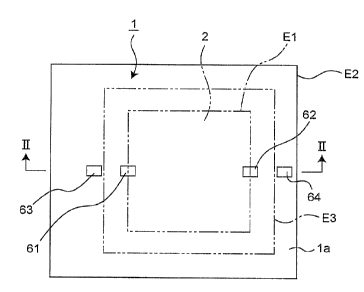
Fig. 1 is a top plan view of a pressure sensor
according to a first embodiment of the present invention;
Fig. 2 is a sectional view taken along the line
II-II in Fig. 1;
Fig. 3 is a circuit diagram of a bridge circuit
for detecting a detection signal, employed in the pressure
sensor of Fig. 1;
Fig. 4 is an explanatory view of the layout of
electrodes and a metal wire in the bridge circuit of
Fig. 3;
Fig. 5 is a sectional explanatory view of a
carbon nanotube used for the bridge circuit of Fig. 3;
Fig. 6 is a sectional view explanatory of the
carbon nanotube of Fig. 5;
Fig. 7 is a view similar to that of Fig. 2,
particularly showing operation of the pressure sensor of
Fig. 1;
Fig. 8 is a top plan view of a pressure sensor
according to a second embodiment of the present invention;
CA 02430451 2003-09-03
S
Fig. 9 is a sectional view taken along the line
IX-IX in Fig. 8;
Fig. 10 is a view similar to Fig. 9,
particularly showing operation of the pressure sensor of
Fig. 8;
Fig. 11 is a top plan view of a pressure sensor
according to a third embodiment of the present invention;
Fig. 12 is a sectional view taken along the
line XII-XII in Fig. 11;
Fig. 13 is a circuit diagram of a bridge
circuit for detecting a detection signal, employed in the
pressure sensor of Fig. 11;
Fig. 14 is a view similar to Fig. 12,
particularly showing operation of the pressure sensor of
Fig. 11;
Fig. 15 is a top plan view of an acceleration
sensor according to a fourth embodiment of the present
invention, the upper glass cap being removed therefrom;
Fig. 16 is a sectional view taken along the
line XVI-XVI in Fig. 15, the upper glass cap being
provided;
Fig. 17 is a view similar to Fig. 16;
particularly showing operation of the acceleration sensor
of Fig. 15;
CA 02430451 2003-09-03
6
Fig. 18 is a top plan view of an acceleration
sensor according to a fifth embodiment of the present
invention, the upper glass cap being removed therefrom:
Fig. 19 is a sectional view taken along the
line XIX-XIX in Fig. 18, the upper glass cap being
provided;
Fig. 20 is a view similar to Fig. 19,
particularly showing operation of the acceleration sensor
of Fig. 18;
Fig. 21 is a top plan view of an acceleration
sensor according to a sixth embodiment of the present
invention, the upper glass cap being removed therefrom;
and
Fig. 22 is a sectional view taken along the
line XXII-XXII in Fig. 21, the upper glass cap being
provided.
Before the description of the present invention
proceeds, it is to be noted that like parts are designated
by like reference numerals throughout several views of the
accompanying drawings.
DETAILED DESCRIPTION OF THE INVENTION
Hereinafter, mechanical deformation amount
sensors according to embodiments of the present invention
are described with reference to the drawings.
c~ ; r r +- o." t-, r, ~ ; ,., o ,-, +
CA 02430451 2003-09-03
As shown in Figs. 1 and 2, a mechanical
deformation amount sensor according to a first embodiment
acts as a pressure sensor for detecting fluid pressure. In
this embodiment, a sensor structure 1 is a so-called
micro-electromechanical systems (MEMS) sensor chip
(semiconductor pressure sensor chip) obtained from a
silicon substrate. The pressure sensor chip 1 is
constituted by a support portion la having the shape of a
rectangular frame and a thin-walled diaphragm 2 occupying
an inside space of the frame of the support portion la. In
this pressure sensor chip 1, the diaphragm 2 acting as a
thin-walled pressure bearing portion is formed by etching
a recess 3 into a portion of a rear face of the pressure
sensor chip 1 by anisotropic etching such that a wall of
the recess 3, namely, the diaphragm 2 has a predetermined
thickness. Thus, as shown in Fig. l, the support portion
la has three rectangular frame edges, i.e., an innermost
rectangular frame edge E1 bounding the diaphragm 2, an
outermost rectangular. frame edge E2 defining an outer
contour of the sensor structure 1 and an intermediate
rectangular frame edge E3 defining a contour of a mouth of
the recess 3. A base 9 made of glass and having a pressure
introduction bore 5 for introducing the fluid pressure
into the recess 3 is secured to the rear face of the
pressure sensor chip 1. In the pressure sensor chip 1,
when the fluid pressure is introduced from the pressure
introduction bore 5 into the recess 3, the diaphragm 2 is
deformed so as to be deflected.
In order t:o transduce an electrical signal from
a deformation amount of the diaphragm 2 in accordance with
magnitude of the fluid pressure, carbon nanotube
resistance elements 51 and 62 are provided on a front face
CA 02430451 2003-09-03
of the diaphragm 2. Each of the carbon nanotube resistance
elements 61 and 62 is provided and fixed at a central
location of each of the opposite sides of the innermost
rectangular frame edge El of the support portion la in a
peripheral edge portion of the diaphragm 2 such that axes
of the carbon nanotube resistance elements 61 and 62 are
aligned with each other. A carbon nanotube has such a
property that when the carbon nanotube is deformed in a
direction perpendicular to an axial or longitudinal
direction of the carbon nanotube, electrical conductivity
(electric resistance) of the carbon nanotube changes in
accordance with the deformation amount. Deflective
deformation of the diaphragm 2 is produced in a thickness
direction of the substrate. Hence, since the axial
direction of the carbon nanotube is orthogonal to the
direction of deflective deformation of the diaphragm 2 by
the above described arrangement of the carbon nanotube
resistance elements 61 and 62, deflective deformation of
the diaphragm 2 is efficiently transmitted to the carbon
nanotube resistance elements 61 and 62 and thus, the
electrical conductivity of the carbon nanotube increases.
Meanwhile, since the carbon nanotube resistance elements
61 and 62 are also provided in the peripheral edge portion
of the diaphragm 2, whose deflective deformation is large,
deflective deformation of the diaphragm 2 is efficiently
transmitted to the carbon nanotube resistance elements 61
and 62, thereby resulting in increase of change of
electrical conductivity of the carbon nanotube.
An overall length of the carbon nanotube
resistance elements 61 and 62 may be placed on the
diaphragm 2. However, in this embodiment, each of the
carbon nanotube resistance elements 61 and 62 is disposed
so as to stride over, at its longitudinal middle portion,
CA 02430451 2003-09-03
9
the boundary E1 of the diaphragm 2 and the support portion
1 a such that a substantially half portion of each of the
carbon nanotube resistance elements 61 and 62 are placed
on the diaphragm 2. This is because the diaphragm 2 is
subjected to large deflective deformation in the
neighborhood of the boundary E1 of the diaphragm 2 and the
support portion 1a so as to flex.
Meanwhile, as shown in Fig. 3, a bridge circuit
for detecting a detection signal is formed by the carbon
nanotube resistance elements 61 and 62 and reference
resistance elements 63 and 64. Each of the reference
resistance elements 63 and 64 is provided and fixed on the
front face of the support portion la which is not deformed
by the fluid pressure. The axes of the reference
resistance elements 63 and 64 are aligned with those of
the carbon nanotube resistance elements 61 and 62. Carbon
nanotubes are used as material of the reference resistance
elements 63 and 64. The resistance elements 61 to 69 made
of the carbon nanot.ubes are formed so as to have an
identical electric resistance when no pressure is applied
to the diaphragm 2. By using identical carbon nanotubes
61-64 having an identical resistance, the detection
accuracy of the bridge circuit is improved.
In the bridge circuit, the carbon nanotube
resistance elements 61 and 62 which are deformed in
response to deformation of the diaphragm 2 are,
respectively, disposed on a pair of opposite sides of the
innermost rectangular frame edge El of the support portion
la. The reference resistance elements 63 and 64 are
respectively provided outside a pair of opposite sides of
the intermediate rectangular frame edge E3 of the support
portion la. A DC voltage Vd is applied between a junction
CA 02430451 2003-09-03
8a of the carbon nanotube resistance element 61 and the
reference resistance element 64 and a junction 8b of the
carbon nanotube resistance element 62 and the reference
resistance element 63. A potential difference between a
5 junction 9a of the carbon nanotube resistance element 61
and the reference resistance element 63 and a junction 9b
of the carbon nanotube resistance element 62 and the
reference resistance element 64 corresponds to the
detection signal.
Fig. 4 shows an example of a wiring pattern 7
for connecting the resistance elements 61 to 64 so as to
form the bridge circuit. In this example, the wiring
pattern 7 is formed on the surface of the sensor structure
1 including the diaphragm 2, while electrode pads for the
input terminals 8a and 8b for applying the DC voltage Vd
to the bridge circuit and electrode pads for the output
terminals 9a and 9b for providing the detection signal are
disposed on the surface of the support portion la. The
wiring pattern 7 cars be formed by a metal wire such as
aluminum but may also be formed through diffusion wiring
by doping the silicon substrate acting as the pressure
sensor chip 1. Alternatively, the wiring pattern may be
formed by combination of the above two procedures.
Fig. 5 schematically shows the layout of a
carbon nanotube 6 for forming the carbon nanotube
resistance elements Eil and 62 and the reference resistance
elements 63 and 64. As shown in Fig. 5, the carbon
nanotube 6 is a rod-like minute structure connected, at
its opposite end portions, to the wiring pattern 7. In
order to form the carbon nanotube 6 at a predetermined
location on the surface of the sensor structure 1, a
method in which a carbon nanotube formed already into a
CA 02430451 2003-09-03
11
rod-like shape is provided and fixed at the predetermined
location. Alternatively, a method in which a carbon
nanotube is grown at. the predetermined location on the
surface of the sensor structure 1 may be employed. In the
former method, a commercially available carbon nanotube
can be used but the sensor structure 1 is minute and size
of the carbon nanotube itself is quite small, so that
handling of the carbon nanotube is not so easy. Hence, the
latter method is preferably employed. In the latter
method, a metal such as iron, nickel and cobalt or a
compound containing one of said metals may be used as a
catalyst and the carbon nanotube formed at the
predetermined location by using the catalyst as a starting
point. For example, in Fig. 5, at the location for
providing the carbon nanotube 6 on the surface of the
pressure sensor chip l, ferric oxide (Fe203) is formed as
catalytic portions. The catalytic portions are disposed
at locations corresponding to opposite end portions of the
carbon nanotube 6 such that the carbon nanotube 6 is
formed between the catalytic portions by such processes as
chemical vapor deposition (CVD) and arc discharge. In
order to form the catalytic portions, resist patterning,
for example, is performed on the surface of the pressure
sensor chip 1 so as to deposit, sputter, drip or spin coat
the catalytic material. Meanwhile, in order to form the
carbon nanotube 6, CVD or arc discharge is performed at a
temperature ranging from 500 to l, 000°C while a mixed gas
composed of hydrocarbon gas such as methane and hydrogen
gas is provided for forming the carbon nanotube 6.
Carbon nanotubes are roughly classified into
single-wall carbon nanotubes (SWNT) and multi-wall carbon
nanotubes (MWNT). Single-wall carbon nanotubes are a
cylindrical substance formed by a single graphite sheet.
CA 02430451 2003-09-03
12
On the other hand, multi-wall carbon nanotubes are a
cylindrical substance formed by a plurality of graphite
sheets provided concentrically or in a scroll. The carbon
nanotube 6 employed i.n the present invention is preferably
a single-wall carbon nanotube but may also be a multi-wall
carbon nanotube. However, since change of electrical
conductivity of single-wall carbon nanotubes upon its
deformation in the direction orthogonal to the
longitudinal direction is larger than that of multi-wall
carbon nanotubes, single-wall carbon nanotubes are more
advantageous for achieving high sensitivity than multi-
wall carbon nanotubes. In this embodiment, each of the
resistance elements 61 to 64 employing the carbon
nanotubes 6 is formed by a plurality of single-wall carbon
nanotubes which are arranged side by side and are
electrically connected to each other in parallel. As a
result, since scattering degrees of change of the
electrical conductivity of the respective single-wall
carbon nanotubes are averaged so as to be restrained, not
only high sensitivity can be gained but detection accuracy
can be improved.
In this embodiment, each of the opposite end
portions of the carbon nanotube 6 is covered by a metal
electrode 10 extending from the wiring pattern 7 and made
of aluminum or titanium/gold. By providing the metal
electrode 10, the opposite end portions of the carbon
nanotube 6 and the wiring pattern 7 can be connected to
each other positively. In addition, since the metal
electrode 10 grips each of the opposite end portions of
the carbon nanotube 6, the carbon nanotube 6 is firmly
fixed so as to be prevented from being removed from the
predetermined location on the surface of the chip 1.
CA 02430451 2003-09-03
13
In this embodiment, a surface of the carbon
nanotube may also be covered by an insulating coating
6
film 13 as shown in Fig. 6. The insulating coating film
13
protects
the carbon
nanotube
6 and secures
the carbon
nanotube to the pressure sensor chip 1 more firmly. The
6
insulating coating film 13 may be provided so as to cover
the carbon nanotube 6 spottily but a passivation film
provided
on the surface
of the pressure
sensor chip
1 may
be used as
the insulating
coating
film 13.
Thus, the
insulating coating film 13 not only protects the surface
of the sensor
chip 1 but
protects
and secures
the carbon
nanotube As shown in Fig. 6, an insulating film 11 made
6.
of silicon dioxide (~i02) or the like is provided on the
surface of the pressure sensor chip 1 formed by the
silicon substrate
and the
carbon nanotube
6 and the
metal
wire of the
wiring pattern
7 are provided
on the
insulating film 11. l.n case the wiring pattern 7 includes
a portion formed by diffusion wiring, the portion of
diffusion
wiring is
disposed
in the pressure
sensor chip
1
under the insulating film 11 but may be electrically
conducted to a surface of the insulating film 11 by
forming a contact hole at a desired location of the
insulating film 1.
In the semiconductor pressure sensor of the
first embodiment, when no fluid pressure is introduced
into the recess 3 from the pressure introduction bore 5 of
the base 4, the potential difference between the output
terminals 9a and 9b of the bridge circuit is zero.
However, if fluid pressure is introduced into the recess 3
from the pressure introduction bore 5 of the base 4, a
central portion of the diaphragm 2 is deflected by the
fluid pressure so as to be expanded upwardly as shown in
Fig. 7 and the peripheral edge portion of the diaphragm 2
CA 02430451 2003-09-03
14
is deformed so as to be pulled obliquely upwardly. Thus,
the carbon nanotube resistance elements 61 and 62 fixed at
the peripheral edge portion of the diaphragm 2 are
subjected to compressive deformation in a direction
orthogonal to their axial direction,i.e. in a direction of
small modulus of elasticity in response to deformation of
the peripheral edge portion of the diaphragm 2. By this
compressive deformation of the carbon nanotube resistance
elements 61 and 62, electric resistance, i.e., electrical
conductivity between the carbon nanotube resistance
elements 61 and 62 changes in accordance with amount of
the compressive deformation and a potential difference
corresponding to the change of the electric resistance is
generated between the output terminals 9a and 9b of the
bridge circuit. Since a magnitude of this potential
difference corresponds to a magnitude of the fluid
pressure applied to the diaphragm 2, the fluid pressure
can be detected from this potential difference.
Second embodiment
Figs. 8 and 9 show a semiconductor pressure
sensor according to a second embodiment of the present
invention. In the first embodiment, a surface of the
pressure sensor chip 1 including the diaphragm 2 is flat
and the carbon nanotube resistance elements 61 and 62 are
arranged and fixed on this flat surface of the pressure
sensor chip 1. The second embodiment is designed to make
the best use of such a property of a carbon nanotube that
electric resistance of the carbon nanotube changes greatly
at its location having a large angle of deformation.
Namely, in this embodiment, a step portion 12
is formed at a boundary of the peripheral edge portion,
CA 02430451 2003-09-03
IS
i.e., a deformation portion of the diaphragm 2 and the
support portion 1 a as shown in Fig. 9 such that a surface
of the diaphragm 2 is set lower than that of the support
portion 1 a surrounding the diaphragm 2. Each of the
carbon nanotube resistance elements 61 and 62 is disposed
and fixed so as to longitudinally stride over the step
portion 12 and is bent from the surface of the support
portion la to the surface of the diaphragm 2 along a
vertical surface of the step portion 12. Since other
constructions of the semiconductor pressure sensor of this
embodiment are similar to those of the pressure sensor of
the first embodiment, the description is abbreviated for
the sake of brevity.
In the semiconductor pressure sensor, when
fluid pressure is introduced into the recess 3 from the
pressure introduction bore 5 of the base 4, a central
portion of the diaphragm 2 is deflected by the fluid
pressure so as to be expanded upwardly and the peripheral
edge portion of the diaphragm 2 is deformed so as to be
pulled obliquely upwardly as shown in Fig. 10. Thus, each
of the carbon nanot:ube resistance elements 61 and 62
secured to the step portion 12 in the peripheral edge
portion of the diaphragm 2 is subjected to compressive
deformation in a direction orthogonal to its axial or
longitudinal direction, i.e., in a direction of small
modulus of elasticity in response to deformation of the
peripheral edge portion of the diaphragm 2. At this time,
since a portion of each of the carbon nanotube resistance
elements 61 and 62, which is disposed at the step portion
12, is subjected to compressive deformation at a large
angle, the electric resistance (electrical conductivity)
between opposite ends of each of the carbon nanotube
resistance elements 61 and 62 changes greatly and thus,
CA 02430451 2003-09-03
16
the potential difference between the output terminals 9a
and 9b of the bridge circuit becomes large. Namely, since
a large-level electrical signal can be obtained by the
small deformation amount, the fluid pressure can be
detected at high sensitivity.
Third embodiment
Figs. 11 and 12 show a semiconductor pressure
sensor according to a third embodiment of the present
invention. In the first and second embodiments, the bridge
circuit is formed by providing the reference resistance
elements 63 and 64. In this embodiment, reference
resistance elements 63' and 64' are provided at a central
portion of a surface of the diaphragm 2 such that an axial
direction of the reference resistance elements 63' and 64'
is parallel to that of the carbon nanotube resistance
elements 61 and 62 disposed in the peripheral edge portion
of the diaphragm 2. A bridge circuit shown in Fig. 13 is
formed by using the .reference resistance elements 63' and
64'. The reference resistance elements 63' and 64' are
constituted by carbon nanotubes.
In the semiconductor pressure sensor, when
fluid pressure is introduced into the recess 3 from the
pressure introduction bore 5 of the base 4, a central
portion of the diaphragm 2 is deflected by the fluid
pressure so as to be expanded upwardly and the peripheral
edge portion of the diaphragm 2 is deformed so as to be
pulled obliquely upwardly as shown in Fig. 14. Thus the
reference resistance elements 63' and 64' disposed at the
central portion of the diaphragm 2 are deformed so as to
be stretched, while the carbon nanotube resistance
CA 02430451 2003-09-03
17
elements 61 and 62 fixed at the peripheral edge portion of
the diaphragm 2 are subjected to compressive deformation
in a direction orthogonal to an axial direction of the
carbon nanotube resistance elements 61 and 62, i.e., in a
direction of small modulus of elasticity in response to
deformation of the peripheral edge portion of the
diaphragm 2. A direction of change of electric resistance
of the carbon nanotube resistance elements 61 and 62 is
opposite to that of the reference resistance elements 63'
and 64' .
Thus, potential difference produced between the
output terminals 9a and 9b of the bridge circuit becomes
larger than that of the first embodiment. Namely, since a
large-level electrical signal can be obtained by the small
deformation amount, the fluid pressure can be detected at
higher sensitivity.
Fourth embodiment
Figs. 15 and 16 show an acceleration sensor
according to a fourth embodiment of the present invention.
In the first to third embodiments, the mechanical
deformation amount sensor acted as a pressure sensor. In
this fourth embodiment, the mechanical deformation amount
sensor acts as the acceleration sensor. By performing
micromachining such as etching on a silicon substrate as
shown in Fig. 15, an acceleration sensor chip 20 is
formed. This acceleration sensor chip 20 includes a frame-
like support portion 21 and a weight portion 22 whose one
side is integrally attached to the support portion 21 by a
pair of parallel beam portions 23. The weight portion 22
is pivotally provided in a space surrounded by the support
CA 02430451 2003-09-03
18
portion 21. As shown in Fig. 16, a metallic film 24 is
provided on an upper: surface of the support portion 21
along an outer peripheral portion of the acceleration
sensor chip 20. An upper glass cap 26 formed with a recess
25 enabling upward movement of the weight portion 22, is
provided on an upside of the acceleration sensor chip 20.
The underside of this upper glass cap 26 is bonded to the
outer peripheral portion of the upside of the acceleration
sensor chip 20 via the metallic film 24.
A lower glass cap 28 formed with a recess 27
enabling downward movement of the weight portion 22 is
secured to an underside of the acceleration sensor chip
20. An outer peripheral portion of an upside of the lower
glass cap 28 is bonded to the underside of the support
portion 21 of the acceleration sensor chip 20 by anodic
bonding.
The carbon nanotube resistance elements 61 and
62 are fixed to the beam portions 23 acting as a
deformation portion which is deformed by pivotal movement
of the weight portion 22. The carbon nanotube resistance
elements 61 and 62 are disposed so as to axially or
longitudinally stride over the beam portions 23 and the
weight portion 22 such that an axial direction of the
carbon nanotube resistance elements 61 and 62 is
orthogonal to a direction of deformation of the beam
portions 23. Meanwhile, the reference resistance elements
63 and 64 formed by carbon nanotubes are secured to an
upside of the weight portion 22 so as to axially extend
orthogonally to the axial direction of the carbon nanotube
resistance elements 61 and 62. The resistance elements 61
to 64 are fixed to the acceleration sensor chip 20 in the
same manner as the first embodiment. Although a metal
CA 02430451 2003-09-03
19
wire for effecting bridge connection of the resistance
elements 61 to 64 in the same manner as depicted in Fig. 3
is formed on the surface of the support portion 21, the
weight portion 22 and the beam portions 23 and input and
output electrodes of the bridge circuit are formed on the
surface of the support portion 21, these circuit
components are not shown in Figs. 15 and 16. In Fig. 16,
stoppers 29 and 30 for restraining movement of the weight
portion 22 are, respectively, provided on the upper glass
cap 26 and the lower glass cap
28.
If an acceleration is applied to the
acceleration sensor in the direction of the arrow Y as
shown in Fig. 17, a force corresponding to the
acceleration is applied to the weight portion 22 so as to
pivot the weight portion 22 as shown. By this pivotal
movement of the weight portion 22, the beam portions 23
for coupling the support portion 21 and the weight portion
22 with each other are subjected to deflective deformation
and thus, the carbon nanotube resistance elements 61 and
62 are also deformed in response to this deflective
deformation of the beam portions 23.
A deformation amount of the carbon nanotube
resistance elements 61 and 62 corresponds to a magnitude
of the acceleration and the electric resistance
(electrical conductivity) between opposite ends of the
carbon nanotube resistance elements 61 and 62 changes in
response to this deformation amount. Thus, potential
difference corresponding to the change of electric
resistance is produced between the output terminals 9a and
9b of the bridge circuit as shown in Fig. 3. Since the
magnitude of this potential difference corresponds to the
CA 02430451 2003-09-03
magnitude of the acceleration applied to the weight
portion 22, the acceleration can be detected from the
potential difference.
5
Fifth embodiment
Figs. 18 and 19 show an acceleration sensor
according to a fifth embodiment of the present invention.
10 In this embodiment, a step portion 23a is formed on an
upside of the beam portion 23 by setting a surface of the
support portion 21 higher than that of the weight portion
22 as shown in Figs. 18 and 19. Each of the carbon
nanotube resistance elements 61 and 62 is disposed and
15 fixed so as to stride over the step portion 23a from the
surface of the support portion 21 to the surface of the
weight portion 22.
Namely, in the same manner as the step portion
20 12 of the second embodiment, a large change of electric
resistance of the carbon nanotube resistance elements 61
and 62 is obtained upon deformation of the beam portions
23 in order to increase sensor sensitivity. Since a
function of the step portion 23a is identical with that of
the step portion 12 of the second embodiment, the
description is not repeated for sake of brevity. Also,
since operation of the acceleration sensor at the time an
acceleration is applied thereto in the direction of the
arrow Y as shown in Fig. 20 is similar to that of the
fourth embodiment, the description is not repeated for
sake of brevity.
CA 02430451 2003-09-03
21
Figs. 21 and 22 show an acceleration sensor
according to a sixth embodiment of the present invention.
In the acceleration sensors of the fourth and fifth
embodiments, the reference resistance elements 63 and 64
formed by the carbon nanotubes are provided on the upside
of the weight portion 22. In this embodiment, the
reference resistance elements 63' and 64' are fixed to the
beam portions 23 as shown in Figs. 21 and 22 such that
axes of the reference resistance elements 63' and 64' are
orthogonal to those of the carbon nanotube resistance
elements 61 and 62. The bridge circuit shown in Fig. 13 is
constituted by the rE:sistance elements 61, 62, 63' and 64'
formed by carbon nanotubes. Since other constructions of
the acceleration sensor are similar to those of the fourth
embodiment, the description is not repeated for sake of
brevity.
The embodiments have been described above as
concrete examples of the present invention. However, it is
needless to say that the present invention is not limited
to these embodiments but may be modified variously. For
example, in case the reference resistance elements are
used in the above embodiments, the reference resistance
elements may be replaced by diffused resistors. Meanwhile,
in the above embodiments, the MEMS sensor employing the
silicon substrate is recited as an example but may be
replaced by a sensor structure formed by a substrate made
of another semiconductor material. In the present
invention, since the carbon nanotubes are used as the
detection elements, there is no restriction that a
semiconductor substrate should be used as the substrate as
in a configuration based on piezoelectric resistance. A
substrate made of an insulating material such as glass can
also be used.
CA 02430451 2003-09-03
22
Furthermore, the above embodiments were
directed to pressure sensors and acceleration sensors.
However, other sensors such as, for example, tactile
sensors for detecting contact pressure, sound wave sensors
(microphone) for detecting air pressure, ultrasonic
sensors, sensors for detecting pressure changes in a human
body may also be developed using mechanical deformation
amount sensor technology.
By the above described arrangement of the
mechanical deformation amount sensor of the present
invention, the physical quantity can be detected based on
electrical characteristics of the carbon nanotube at
higher sensitivity than in prior art sensors. Namely, when
the physical quantity to be detected by the sensor is
applied to the sensor structure in a state where the
voltage is applied to the carbon nanotube resistance
element via the wiring pattern, the deformation portion is
initially deformed and then, the carbon nanotube
resistance element is mechanically deformed in response to
the deformation of the deformation portion. The carbon
nanotube has a property that its electrical conductivity
(electric resistance) changes upon its mechanical
deformation. Since quantity of change of its electrical
conductivity is quite large in comparison with
piezoelectric resistance, the electrical conductivity of
the carbon nanotube resistance element changes rather
greatly upon its mechanical deformation, so that quantity
of change of voltage or electric current due to the change
of the electrical conductivity becomes comparatively large
and is converted, through the wiring pattern, into a
highly sensitive electrical signal. Since this electrical
signal is used as an. index indicative of magnitude of the
physical quantity to be detected and is converted into the
CA 02430451 2003-09-03
23
physical quantity, the physical quantity can be detected
at high sensitivity.
In the present invention, if the deformation
portion is subjected to mechanical deformation when the
physical quantity to be detected is applied to the sensor
structure, the deformation portion is not specifically
restricted in shape, etc. For example, the deformation
portion can be so formed as to be thinner than the support
portion and is deformed so as to be deflected elastically
when the physical quantity is applied to the sensor
structure.
Meanwhile, in the present invention, the sensor
structure is preferably a so-called micro-electro-
mechanical systems (MEMS) sensor chip formed by
micromachining a silicon substrate. In the present
invention employing the carbon nanotube which is a quite
minute element, the MEMS sensor chip is very advantageous
for achieving both high sensitivity and compactness. In
this case, the carbon nanotube resistance element is
preferably provided on the deformation portion through an
insulating film.
Furthermore, in the present invention, the
carbon nanotube resistance element is preferably disposed
such that a longitudinal direction of the carbon nanotube
resistance element is orthogonal to a direction of
deformation of the deformation portion. The carbon
nanotube has a property that its electrical conductivity
changes upon its deformation in a direction orthogonal to
its longitudinal direction. Since the longitudinal
direction of the carbon nanotube resistance element is
orthogonal to the direction of deformation of the
CA 02430451 2003-09-03
24
deformation portion, deformation of the deformation
portion is reflected most precisely in deformation of the
carbon nanotube resistance element. As a result, change of
electrical conductivity of the carbon nanotube resistance
element increases accordingly, which is advantageous for
achieving high sensitivity.
Additionally, in the present invention, the
wiring pattern may have, at its end portion connected to
the carbon nanotube resistance element, a metal electrode
such that each of opposite end portions of the carbon
nanotube resistance element is covered by the metal
electrode. Thus, the carbon nanotube resistance element
can be positively connected to the wiring pattern by the
metal pattern and the carbon nanotube resistance element
can be securely fixed to the deformation portion.
Meanwhile, in the present invention, a surface
of the carbon nanotube resistance element is preferably
covered by an insulating coating film. This is because the
insulating coating film can not only protect the carbon
nanotube resistance element but fix the carbon nanotube
resistance element to the deformation portion more
securely. In this case, the insulating coating film may be
formed by a passivation film provided on a surface of the
sensor structure so as to not only protect the surface of
the sensor structure but protect and fix the carbon
nanotube resistance element.
Also, in the present invention, it is
preferable that a step portion be formed on the
deformation portion and the carbon nanotube resistance
element be provided on the deformation portion so as to
stride over the step portion.
CA 02430451 2003-09-03
Thus, the change of the electrical conductivity
of the carbon nanotube at its portion having a large angle
of deformation is large as compared with a case in which
5 the carbon nanotube resistance element is provided on a
flat face. A large change of electrical conductivity can
be obtained in response to a small deformation amount and
thus, higher sensitivity can be achieved.
10 Meanwhile, in the present invention, it is
preferable that a reference resistance element be provided
at a portion of the sensor structure other than the
deformation portion and that the reference resistance
element and the carbon nanotube resistance element be
15 connected to each other by the wiring pattern so as to
form a bridge circuit. In this case, a voltage is applied
to an input terminal of the bridge circuit and a voltage
of an output terminal of the bridge circuit can be
detected as an electrical signal corresponding to a change
20 of electrical conductivity of the carbon nanotube
resistance element upon mechanical deformation of the
carbon nanotube resistance element. High sensitivities
can be gained and detection accuracy improved. In this
case, the reference resistance element is preferably
25 formed by a carbon nanotube. When both the detective
resistance element and the reference resistance element
are identically formed by the carbon nanotubes, detection
accuracy is improved further.
Meanwhile, in the present invention, the carbon
nanotube resistance element is preferably formed by a
single-wall carbon nanotube. This is because change of
electrical conductivity of the single-wall carbon nanotube
upon its deformation in a direction orthogonal to its
CA 02430451 2006-04-18
26
longitudinal direction is larger than that of a multi-wall
carbon nanotube. In this case, it is preferable that the
carbon nanotube resistance element be formed by a
plurality of the single-wall carbon nanotubes which are
arranged side by side and are electrically connected to
each other in parallel. Thus, since scattering degrees of
change of electrical conductivity of the respective s
single-wall carbon nanotubes are averaged so as to be
restrained, not only high sensitivity can be gained but
detection accuracy can be improved.
Furthermore, in the present invention, an
acceleration sensor having an acceleration as the physical
quantity to be detected is provided as one concrete
example of the mechanical deformation amount sensor. In
the acceleration sensor, the sensor structure further
includes a weight portion integrally coupled with the
support portion by the deformation portion.
Moreover, in the present invention, a pressure
sensor having a fluid pressure as the physical quantity to
be detected is provided as another concrete example of the
mechanical deformation amount sensor. In the sensor
structure of the pressure sensor, the support portion is
formed in a shape of a frame and the deformation portion
is formed by a diaphragm occupying an inside space of the
frame of the support portion such that the diaphragm bears
the fluid pressure. In this case, the carbon nanotube
resistance element is preferably provided at a peripheral
edge portion of the diaphragm.
As is clear from the foregoing description,
mechanical deformation amount sensors of the present
invention can detect, as an electrical signal based on
CA 02430451 2003-09-03
27
change of electrical conductivity of carbon nanotube
resistance elements, magnitude of a physical quantity
applied to the sensor structure. Such a remarkable effect
is gained by utilizing electrical characteristics of the
carbon nanotube. The physical quantity can be detected at
higher sensitivity than prior art configurations
employing, for example, a piezoelectric resistance
element.