Note: Descriptions are shown in the official language in which they were submitted.
,_. ~ 02438577 2004-07-27 '')
J.
WO 02!067327 PCT/CA02/00173
1
PIXEL CURRENT DRIVER FOR ORGANIC LIGHT EMITTING DIODE DISPLAYS
BACKGROUND OF THE INVENTION
!.Field of the Invention
The present invention relates to an organic light
emitting diode disglay, and more particularly to w a pixel
current driver for an organic light emitting diode (OLED),
_ _ _ _ _ _._. _._. _- _._ _ ._ _._ . _ _____._ _
2.Description of the Prior Art
OLED displays have gained significant interest recently
in display applications in view of their faster response
times, larger viewing angles, higher contrast, lighter weight,
lower power, amenability to flexible substrates, as compared
to liquid crystal displays (LCDs). Despite the OLED's
demonstrated superiority over the LCD, there still remain
2o several challenging issues related to encapsulation and
lifetime, yield, color efficiency, and drive electronics, all
of which are receiving considerable attention. Although
passive matrix addressed OLED displays are already in the
marketplace, they do not support the resolution needed in the
next generation displays, since high information content CHIC)
formats are only possible with the active matrix addressing
scheme. Active matrix addressing involves a layer of backplane
electronics, based on thin-film transistors (TFTs) fabricated
using amorphous silicon (a-Si:Ii), polycrystalline silicon
(poly-Si), or polymer technologies, to provide the bias
voltage and drive current needed in each OLED based pixel.
Here, the voltage on each pixel is lower and the current
throughout the entire frame period is a low constant value,
thus avoiding the excessive peak driving and leakage
currents associated with
CA 02438577 2004-07-27
WO 02/067327 PCT/CA02/00173
2
passive matrix addressing. This in turn increases the lifetime
of the OLED.
In active matrix OLED (AMOLED) displays, it is important to
ensure that the aperture ratio or fill factor (defined as the
ratio of light emitting display area to the total pixel area)
should be high enough to ensure display quality. Conventional
AMOLED displays are based on light emission through an
aperture on the glass substrate where the backplane
electronics is integrated. Increasing the on-pixel density of
10- TFT integration for stable drive current reduces the size of
the aperture. The same happens when pixel sizes are scaled
down. One solution to having an aperture ratio that is
invariant on scaling or on-pixel integration density is to
vertically stack the OLED layer on the backplane electronics,
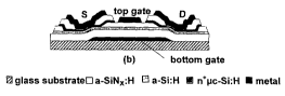
along with a transparent top electrode (see Fig. 2). In Fig.
2, reference numerals S and D denote a source and a drain
respectively. This implies a continuous back electrode over
the OLED pixel. However, this continuous back electrode can
give rise to parasitic capacitance, whose effects become
significant when the electrode runs over the switching and
other thin film transistors (TFTs). Here, the presence of the
back electrode can induce a parasitic channel in TFTs giving
rise to high leakage current. The leakage current is the
current that flows between source and drain of the TFT when
the gate of the TFT is in its OFF State.
SUMMARY OF THE INVENTION
Accordingly, it is an object of the present invention to
provide a pixel current driver for an organic light emitting
34 display (OLED).
To achieve the above object, a pixel current driver for
the OLED layer, according to an aspect of the present
invention, comprises a plurality of thin, film transistors
(TFTs) .
CA 02438577 2004-07-27
WO 02/067327 PCT/CA02/00173
3
Each of the thin film transistor may be an a-Si:H
based thin film transistor or a polysilicon-based thin film
transistor.
The pixel current driver is a current mirror based
pixel current driver for automatically compensating for
shifts in the Vth of each of the thin film transistor in a
pixel and the pixel current driver is for monochrome
displays or for full colour displays.
The circuits are fabricated using normal inverted
staggered TFT structures. Preferably, the length is 30~un
and the width is 1600um. The length and .width of the
transistors may change depending on the maximum drive
current required by the circuit and the fabrication
technology used. The plurality of thin film transistors may
be four thin film transistors formed in a current-programmed
oVT-compensated manner. The OLED layer is vertically
stacked on the plurality of thin film transistors.
With the above structure on an a-Si:H current driver
according to an aspect of the present invention, the charge
induced in the top channel of the TFT is minimized, and the
leakage currents in the TFT is minimized so as to enhance
circuit performance.
BRIEF DESCRIPTION OF THE DRAWINGS
The above objects and features of the present
invention will become more apparent by describing in detail
preferred
CA 02438577 2003-08-18
WO 02/067327 PCT/CA02/00173
4
embodiments thereof with reference to the attached drawings in
which:
Fig. 1 shows variation of required pixel areas with
mobility for 2-T and 5-T pixel drivers;
Fig. 2 shows a pixel architecture for surface emissive a-
Si:H AMOLED displays;
Fig. 3 shows a cross section of a dual-gate TFT structure;
Fig. 4 shows forward and reverse transfer characteristics
of dual-gate TFT for various top gate biases;
Fig. 5A and Fig. 5B show an equivalent circuit for a 2-T
pixel driver and its associated input-output timing diagrams;
Fig. 6A and Fig. 6B show an equivalent circuit for a 5-T
pixel driver and its associated input-output timing diagrams;
Fig. 7 shows transient performance of the 5-T driver for
three consecutive write cycles;
Fig. 8 shows input-output transfer characteristics for the
2-T pixel driver for different supply voltages;
Fig. 9 shows input-output transfer characteristics for the
5-T pixel driver for different supply voltages;
Fig. 10 shows variation in OLED current as a function of
the normalised shift in threshold voltage;
Fig. 11 shows a 2-T polysilicon based pixel current driver
having p-channel drive TFTs;
Fig. 12 shows a 4-T pixel current driver for OLED displays;
CA 02438577 2003-08-18
WO 02/067327 PCT/CA02/00173
Fig. 13 shows a 4-T pixel current driver with a lower
discharge time;
Fig. 14 shows a 4-T pixel current driver without non-linear
5 gain;
Fig. 15 shows a 4-T pixel current driver that is the
building block for the full color circuit; and
Fig. 16 shows a full color(RGB) pixel current driver for
OLED displays.
DETAILED DESCRIPTION OF THE PREFERRED EMBODIMENTS
Although amorphous Si does not enjoy equivalent
electronic properties compared to poly-Si, it adequately meets
many of the drive requirements fox small area displays such as
those needed in pagers, cell phones, and other mobile devices.
Poly-Si TFTs have one key advantage in that they are able to
provide better pixel drive capability because of their higher
mobility, which can be of the order of ~.FE~100cm2/Vs. This makes
poly-Si highly desirable for large area (e.g. laptop size) VGA
and SVGA displays. The lower mobility associated with a-Si:H
TFTs (~,FE-lcm2/Vs) is not a limiting factor since the drive
transistor in the pixel can be scaled up in area to provide
the needed drive current. The OLED drive current density is
typically lOmA/cmz at 10V operation to provide a brightness of
100 cd/m2 - the required luminance for most displays. For
example, with an a-Si:H TFT mobility of 0.5cmz/Vs and channel
length of 25~,m, this drive current requirement translates into
required pixel area of 300 ~m2, which adequately meets the
requirements of pixel resolution and speed for some 3 inch
monochrome display applications. Figure 1 illustrates
simulation results for the variation of the required pixel
size with device mobility calculated for two types of drivers,
CA 02438577 2003-08-18
WO 02/067327 PCT/CA02/00173
6
which will be elaborated later, the 2-T and the 5-T drivers,
wherein ~,o denotes a reference mobility whose value is in the
range 0.1 to 1 cm2/Vs. For instance, the area of the pixel for
the 2-T driver (see Figure 5A) comprises of the area of the
switching transistors, area of the drive transistor, and the
area occupied by interconnects, bias lines, etc. In Fig. 1,
the drive current and frame rate are kept constant at 10~.A and
50Hz, respectively, for a 230 x 230 array. It is clear that
there is no significant savings in area between the 2-T and 5-
T drivers but the savings are considerable with increasing
mobility. This stems mainly from the reduction in the area of
the drive transistor where there is a trade-off between ~,FE and
TFT aspect ratio, W/L(Wide/Length).
In terms of threshold voltage (VT) uniformity and
stability, both poly-Si and a-Si:H share the same concerns,
although in comparison, the latter provides for better spatial
uniformity but not stability (OVT). Thus the inter-pixel
variation in the drive current can be a concern in both cases,
although clever circuit design techniques can be employed to
compensate for ~VT hence improving drive current uniformity. In
terms of long term reliability, it is not quite clear with
poly-Si technology, although there are already products based
on a-Si:H technology for displays and imaging, although the
reliability issues associated with OLEDs may yet be different.
The fabrication processes associated with a-Si:H technology
are standard and adapted from mainstream integrated circuit
(IC) technology, but with capital equipment costs that are
much lower. One of the main advantages of the a-Si:H
technology is that it has become low cost and well-established
technology, while poly-Si has yet to reach the stage of
manufacturability. The technology also holds great promise for
futuristic applications since good as-deposited a-Si:H, a-
SiNX:H, and TFT arrays can be achieved at low temperatures
,.,
CA 02438577 2004-07-27
j
WO 02/067327 PCT/CA02/00173
7
(s120'C) thus making it amenable to plastic substrates, which
is a critical requirement~for mechanically flexible, displays.
To minimize the conduction induced in all TFTs in the pixel
by the back electrode, an alternate TFT structure based on a
dual-gate structure is employed. Tn a dual gate TFT (see Fig.
3), a top gate electrode is added to the TFT structure to
prevent the OLED electrodes from biasing the a-Si:H channel
area (refer to Fig. 2). The .voltage on the top gate can be
chosen such so as to minimize the charge induced in the
(parasitic) top channel of the TFT. The objective underlying
the choice of the voltage on the top gate is to minimize
parasitic capacitance in the driver circuits and leakage
currents in the TFTs so as to enhance circuit performance. In
what follows, the operation of the dual-gate TFT is described,
Figure 3 illustrates the structure of a .dual-gate TFT
fabricated for this purpose, wherein reference numerals S and
D denote a source and a drain respectively. The fabrication
steps are the same as of that of a normal inverted staggered
TFT structure except that it requires a sixth mask for
patterning the top gate. The length of the TFT is around 30~.m
to provide enough spacing between the source and drain for the
top gate, and the width is made very large (1600um) with four
of these TFTs are interconnected in parallel to create a
sizeable leakage current for measurement. A delay time is
inserted in the measurement of the current to ensure that the
measurement has passed the transient period created by defects
in the a-Si:H active layer, which gave rise to a time-
dependent-capacitance., - -
Figure 4 shows results of static current measurements for
four cases:~first when the top gate is tied to -lOV, second
when the top gate is grounded, third when the top gate is
floating, and lastly when the top gate is shorted to the
CA 02438577 2003-08-18
WO 02/067327 PCT/CA02/00173
8
bottom gate. With a floating top gate, the characteristics are
almost similar to that of a normal single gate TFT. The
leakage current is relatively high particularly when the top
gate is biased with a negative voltage. The lowest values of
leakage current are obtained when the top gate is pegged to
either OV or to the voltage of the bottom gate. In particular,
with the latter the performance of the TFT in the (forward)
sub-threshold regime of operation is significantly improved.
This enhancement in sub-threshold performance can be explained
by the forced shift of the effective conduction path away from
the bottom interface to the bulk a-Si:H region due to the
positive bias on the top gate. This in turn decreases the
effect of the trap states at the bottom interface on the sub-
threshold slope of the TFT.
It should be noted that although the addition of another
metal contact as the top gate reduces the leakage current of
the TFT, it can potentially degrade pixel circuit performance
by possible parasitic capacitances introduced by vertically
stacking the OLED pixel. Thus the choice of top gate
connection becomes extremely critical. For example, if the top
gates in the pixel circuit are connected to the bottom gates
of the associated TFTs, this gives rise to parasitic
capacitances located between the gates and the cathode, which
can lead to undesirable display operation (due to the charging
up of the parasitic capacitance) when the multiplexer 0/P
drives the TFT switch. On the other hand, if the top gates are
grounded, this results in the parasitic capacitance being
grounded to yield reliable and stable circuit operation.
The OLED drive circuits considered here are the well
known voltage-programmed 2-T driver and the more sophisticated
current-programmed ~VT-compensated 5-T version (see Figs. 5A
and 6A). The latter is a significant variation of the previous
designs, leading to reduced pixel area (<300~.m), reduced
leakage, lower supply voltage (20V), higher linearity (~30dB),
CA 02438577 2004-07-27
l
WO 02/067327 PCT/CA02/00173
9
and larger dynamic range (.-40dB) . Before discussing on the
operation of the 5-T driver,. the operation of the. relatively
simple voltage-driven 2-T driver is described. Fig. 5B shows
input-output timing diagrams of the 2-T pixel driver. When the
address line is activated, the voltage on the data line starts
charging capacitor Cs and the gate capacitance of the driver
transistor TZ. Depending on the voltage on the data line, the
capacitor charges up to turn the driver transistor TZ on, which
then starts conducting to drive the OLED with the appropriate
level of current. When the address line is turned off, T1 is
turned off but the voltage at the gate of TZ remains since the
leakage current of Tl is trivial in comparison. Hence, the
current through the OLED remains unchanged after the turn off
process. The OLED current changes only the next time around
when a different voltage is written into the pixel.
Unlike the previous driver, the data that is written into
the 5-T pixel in this case is a current (see Fig. 6A). Fig. 6B
shows input-output timing diagrams of a 5-T pixel driver. The
address line voltage, Vaddress and Iota are activated or
deactivated simultaneously. When Vaaaress is activated, it forces
T,, and T2 to turn on. Tl immediately starts conducting but TZ
does not since T, and T4 are off. Therefore, the voltages at
the drain and source of TZ become equal. The current flow
through T1 starts charging the gate capacitor of transistors T,
and TS, very much like the 2-T driver. The current of these
transistors start increasing and consequently TZ starts to
conduct current . Therefore, Tl' s share of Iota reduces and Tz' s
share of Iota increases. This process continues until the gate
capacitors of T3 and TS charge (via T1) to a voltage that forces
- - the current of T3- to- be- Iota. At this time, -the eur-rent -of - T1 - is
zero and the entire Iota goes through TZ and T3. At the same
time, TS drives a current through the OLED, which is ideally
equal to I~ta* (WS/W3) , which signifies a current gain. Now if
Idata and vaaareeg are deactivated, TZ will turn off, but due to
CA 02438577 2003-08-18
WO 02/067327 PCT/CA02/00173
the presence of capacitances'in T3 and T5, the current of these
two devices cannot be changed easily, since the capacitances
keep the bias voltages constant. This forces T4 to conduct the
same current as that of T3, to enable the driver TS to drive
5 the same current into the OLED even when the write period is
over. Writing a new value .into the pixel then changes the
current driven into the OLED.
The result of transient simulation for the 5-T driver
circuit is shown in Fig. 7. As can be seen, the circuit has a
10 write time of <70~,s, which is acceptable for most
applications. The 5-T driver circuit does not increase the
required pixel size significantly (see Fig. 1) since the sizes
of T2, T3, and T4 are scaled down. This also provides an
internal gain (WS/W3 = 8), which reduces the required input
current to <2/~A for 10~,A OLED current. The transfer
characteristics for the 2-T and 5-T driver circuits are
illustrated in Figs. 8 and 9, respectively, generated using
reliable physically-based TFT models for both forward and
reverse regimes. A much improved linearity (~30dB) in the
transfer characteristics (Idata/IoLSD) is observed for the 5-T
driver circuit due to the geometrically-defined internal pixel
gain as compared to similar designs. In addition, there are
two components (OLED and TS) in the high current path, which in
turn decreases the required supply voltage and hence improves
the dynamic range. According to Figure 9, a good dynamic range
(~40dB) is observed for supply voltage of 20V and drive
currents in the range IpLEDSIO~A, which is realistic for high
brightness. Figure 10 illustrates variation in the OLED
current with the shift in threshold voltage for the 2-T and 5-
T driver circuits. The 5-T driver circuit compensates for the
shift in threshold voltage particularly when the shift is
smaller than 10% of the supply voltage. This is because the 5-
T driver circuit is current-programmed. In contrast, the OLED
current in the 2-T circuit changes significantly with a shift
CA 02438577 2003-08-18
WO 02/067327 PCT/CA02/00173
11
in threshold voltage. The 5-T driver circuit described here
operates at much lower supply voltages, has a much larger
drive current, and occupies less area.
The pixel architectures are compatible to surface (top)
emissive AMOLED displays that enables high on-pixel TFT
integration density for uniformity in OLED drive current and
high aperture ratio. A 5-T driver circuit has been described
that provides on-pixel gain, high linearity (~30dB), and high
dynamic range (~40dB) at low supply voltages (15-20V) compared
to the similar designs (27V). The results described here
illustrate the feasibility of using a-Si:H for 3-inch mobile
monochrome display applications on both glass and plastic
substrates. With the latter, although the mobility of the TFT
is lower, the size of the drive transistor can be scaled up
yet meeting the requirements on pixel area as depicted in Fig.
1.
Polysilicon has higher electron and hole mobilities than
amorphous silicon. The hole mobilities are large enough to
allow the fabrication of p-channel TFTs.
The advantage of having p-channel TFTs is that bottom
emissive OLEDs can be used along with a p-channel dxive TFT to
make a very good current source. One such circuit is shown in
Fig. 11. Tn Fig. 11, the source of the p-type drive TFT is
connected to Vdd. Therefore, Vgs, gate-to-source voltage, and
hence the drive current of the p-type TFT is independent of
OLED characteristics. In other words, the driver shown in Fig.
11 performs as a good current source. Hence, bottom emissive
OLEDs are suitable for use with p-channel drive TFTs, and top
emissive OLEDs are suitable for use with n-channel TFTs.
The trade-off with using polysilicon is that the process
of making polysilicon TFTs requires much higher temperatures
than that of amorphous silicon. This high temperature
processing requirement greatly increases the cost, and is not
amenable to plastic substrates. Moreover, polysilicon
CA 02438577 2003-08-18
WO 02/067327 PCT/CA02/00173
12
technology is not as mature and widely available as amorphous
silicon. In contrast, amorphous silicon is a well-established
technology currently used in liquid crystal displays (LCDs).
It is due to these reasons that amorphous silicon combined
with top emissive OLED based circuit designs is most promising
for AMOLED displays.
Compared to polysilicon TFTs, amorphous silicon TFTs are
n-type and thus are more suitable for top emission circuits as
shown in Fig. 2. However, amorphous silicon TFTs have inherent
stability problems due to the material structure. In amorphous
silicon circuit design, the biggest hurdle is the increase in
threshold voltage Vth after prolonged gate bias. This shift is
particularly evident in the drive TFT of an OLED display
pixel. This drive TFT is always in the 'ON' state, in which
there is a positive voltage at its gate. As a result, its Vtn
increases and the drive current decreases based on the
current-voltage equation below:
Ids = ( ~.CoXW / 2L ) (Vgs -Vth) z (in Saturation region)
In the display, this would mean that the brightness of
the OLED would decrease over time, which is unacceptable.
Hence, the 2-T circuits shown earlier are not practical for
OLED displays as they do not compensate for any increase in
Vth~
The first current mirror based pixel driver circuit is
presented, which automatically compensated for shifts in the
Vth of the drive TFT in a pixel. This circuit is the 5-T
circuit shown in Fig. 6A.
Four more OLED pixel driver circuits are presented for
monochrome displays, and one _circuit for full colour displays.
All these circuits have mechanisms that automatically
compensate for Vth shift. The first circuit shown ~in Fig. 12 is
a modification of the 5-T circuit of Fig. 6A. (Transistor T4
has been removed from the 5-T circuit). This circuit occupies
_a smaller area than the 5-T circuit, and provides a higher
CA 02438577 2004-07-27
WO 02/067327 . PCTICA02100173
13
dynamic range. The higher dynamic range allows for a larger
signal swing at the input, which means that the OLED
brightness-can be adjusted over a larger range.
Fig. 12 shows a 4-T pixel driver circuit for ~OLED
displays. The circuit shown in Fig. 13 is a 4-T pixel driver
circuit based on a current mirror. The advantage of this
circuit is that the ,discharge time of the capacitor Cs is
substantially reduced. This is because the discharge path has
two TFTs (as compared to three TFTs in the circuit of Fig.
12). The charging time remains the same. The other advantage
is that there is an additional gain provided by this circuit
because T, and T4 do not nave the same source voltages.
However, this gain is non-linear and may not be desirable in
some cases.
In Fig. 14, another 4-T circuit is shown. This circuit
does not- have the non-linear gain present in the previous
circuit (Fig. 13) since the source terminals of T3 and T4 are
at the same. voltage. It still maintains the lower capacitance
discharge time, along with the other features of the circuit
of Fig. 8.
Fig. 15 shows another version of the g-T circuit. This'
circuit is does not have good current mirror properties.
However, this circuit forms the building block for the 3
colour RGB 'circuit shown in Fig. 16. It also has a low
capacitance discharge time and high dynamic range.
The full colour circuit shown in Fig. 16 minimizes the
area required by an RGB pixel on a display, while maintaining
the desirable features like threshold voltage shift
compensation, in-pixel current gain, low capacitance discharge
time,,and high dynamic range. .
The dual-gate TFTs are used
in the above-mentioned circuits to enable vertical integration
of the OLSD layers with minimum parasitic effects.
The above-mentioned circuits compensate for the Vth shift when
CA 02438577 2004-07-27
. .: v ,
WO 02/067327 PCT/CA02/00173
14
the circuits ccx~rise single-gate TFTs. In addition, these circuits use
n-type amorphous silicon, TFTs. However, the circuits are '
applicable to polysilicon technology using p-type or n-type
TFTs. These circuits when made in polysilicon can compensate '
for the non-uniformity of the threshold voltage, which is a
problem in this technology. The p-type circuits are conjugates
of the above-mentioned circuits and are suitable for the
bottom emissive pixels.