Note: Descriptions are shown in the official language in which they were submitted.
CA 02448736 2003-11-26
WO 02/098624 PCT/US02/17936
Methods for Manufacturing Three-Dimensional Devices
and Devices Created Thereby
CROSS REFERENCE TO RELATED APPLICATIONS
[1] This application claims priority to, and incorporates by reference in
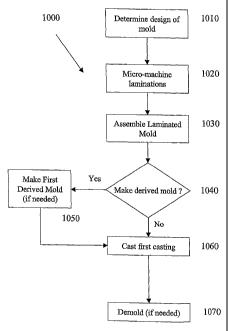
their
entirety, each of: pending U.S. Application Serial No. 60/295,564 (Attorney
Docket No.
MICRO 1 V 1), filed 05 June 2001, and pending U.S. Application Serial No.
60/339,773
(Attorney Docket No. MICRO 2 V 1), filed 17 December 2001.
BR1EF DESCRIPTION OF THE DRAWINGS
[2] The invention and its wide variety of potential embodiments will be more
readily understood through the following detailed description, with reference
to the
accompanying drawings in which:
FIG. 1 is a flowchart of an exemplary embodiment of a method of the present
invention.
FIG. 2 is a flow diagram of exemplary items fabricated using a method of the
presentinvention.
FIG. 3 is a perspective view of an exemplary casting of the present invention
that illustrates aspect ratio.
FIG. 4 is an assembly view of an exemplary assembly of the present invention.
FIG. 5A is a top view of an exemplary stack lamination mold of the present
invention.
FIGS 5B-5E are exemplary alternative cross-sectional views of an exemplary
stack lamination mold of the present invention taken at section lines 5-5 of
FIG.
5A.
FIG. 6 is an unassembled cross-sectional view of an alternative exemplary
stack
lamination mold taken of the present invention at section lines 5-5 of FIG.
5A.
FIG. 7 is a cross-sectional view of an exemplary alternative stack lamination
mold of the present invention taken at section lines 5-5 of FIG. 5A.
FIG. 8 is a perspective view of an exemplary laminated mold.
CA 02448736 2003-11-26
WO 02/098624 PCT/US02/17936
FIG. 9 is a cross-section of an exemplary mold of the present invention taken
along lines 9-9 of FIG 8.
FIG. 10A is a top view an exemplary layer of the present invention having a
redundant array of shapes.
FIG. 10B is a top view of an exemplary layer of the present invention having a
non-redundant collection of shapes.
FIG. 11 is a top view of an exemplary stacked lamination mold of the present
invention.
FIG. 12 is a cross-sectional view of an exemplary mold of the present
invention
taken at section lines 12-12 of FIG. 11.
FIG. 13 is a side view of an exemplary cast part of the present invention
formed
using the exemplary mold of FIG. 11.
FIG. 14 is a top view of an exemplary laminated mold of the present invention.
FIG. 15 is a cross-sectional view of an exemplary mold of the present
invention
taken at section lines 15-15 of FIG.14.
FIG. 16 is a perspective view of an exemplary cast part of the present
invention
formed using the exemplary mold of FIG. 14.
FIG. 17 is a top view of an exemplary planar laminated mold of the present
invention having an array of openings.
FIG. 18 is a top view of an exemplary flexible casting or mold insert of the
present invention molded using the laminated mold of FIG. 17.
FIG. 19 is a top view of an exemplary mold fixture of the present invention
FIG. 20 is a top view of an exemplary planar laminated mold of the present
invention.
FIG. 21 is a top view of an exemplary flexible casting or mold insert of the
present invention molded using the laminated mold of FIG. 20.
FIG. 22 is a top view of an exemplary mold fixture of the present invention
FIG. 23 is a perspective view of an exemplary laminated mold of the present
invention.
FIG. 24 is a close-up perspective view of an exemplary single cylindrical
cavity
of an exemplary mold of the present invention.
CA 02448736 2003-11-26
WO 02/098624 PCT/US02/17936
FIG. 25 is a perspective view of an exemplary cast part of the present
invention.
FIG. 26 is a flowchart of an exemplary method of the present invention.
FIG. 27 is a perspective view of a plurality of exemplary layers of the
present
invention.
FIG. 28 is a perspective view of an exemplary laminating fixture of the
present
invention.
FIG. 29 is a top view of stack lamination mold of the present invention that
defines an array of cavities.
FIG. 30 is a cross-section of a cavity of the present invention taken along
section lines 30-30 of FIG. 29.
FIG. 31 is a perspective view of an exemplary single corrugated feedhorn of
the
presentinvention .
FIG. 32 is a side view of an exemplary casting fixture of the present
invention.
FIG. 33 is a side view of an exemplary section of cylindrical tubing of the
present invention that demonstrates the shape of an exemplary fluidic channel
of
the present invention.
FIG. 34 is a top view of an exemplary micro-machined layer of the present
invention.
FIG. 35 is a cross-sectional view of a laminated slit of the present invention
taken along section lines 35-35 of FIG. 34.
FIG. 36 is a side view of a portion of an exemplary flexible cavity insert of
the
presentinvention.
FIG. 37 is a top view of an exemplary base plate of the present invention.
FIG. 38 is a fxont view of a single exemplary flexible cavity insert assembly
of
the present invention.
FIG. 39 is a front view of flexible cavity inserts of the present invention.
FIG. 40 is a top view of a top plate of the present invention.
FIG. 41 is a flowchart of an exemplary embodiment of a method of the present
invention.
FIG. 42A is a top view of an exemplary laminated stack of the present
invention.
3
CA 02448736 2003-11-26
WO 02/098624 PCT/US02/17936
FIG. 42B is a cross-sectional view, taken at section lines 42-42 of FIG. 42A,
of
an exemplary laminated stack of the present invention.
FIG. 43 is side view of an exemplary mold and casting of the present
invention.
FIG. 44 is a top view of an exemplary casting fixture of the present
invention.
FIG. 45 is a front view of the exemplary casting fixture of FIG. 44.
FIG. 46 is a top view of a portion of an exemplary grid pattern of the present
invention.
FIG. 47 is an assembly view of components of an exemplary pixelated gamma
camera of the present invention.
FIG. 48A is a top view of an array of generic rnicrodevices of the present
invention.
FIG. 48B is a cross-sectional view of an exemplary microdevice of the present
invention, taken at section lines 48-48 of FIG. 48A, in the open state.
FIG. 49 is a cross-sectional view of the exemplary microdevice of FIG. 48B,
taken at section lines 48-48 of FIG. 48A, in the closed state.
FIG. 50 is a cross-sectional view of an alternative exemplary microdevice of
the
present invention, taken at section lines 48-48 of FIG. 48A, and shown with an
inlet valve open.
FIG. 51 is a cross-sectional view of the alternative exemplary microdevice of
FIG. 50, taken at section lines 48-48 of FIG. 48A, and shown with an outlet
valve open.
FIG. 52 is a top view of an exemplary microwell array of the present
invention.
FIG. 53 is a cross-sectional view taken at lines 52-52 of FIG. 52 of an
exemplary microwell of the present invention.
FIG. 54 is a cross-sectional view taken at lines 52-52 of FIG. 52 of an
alternative exemplary microwell of the present invention.
FIG. 55 is a top view of exemplary microwell of the present invention.
FIG. 56 is a cross-sectional view of an exemplary microwell of the present
invention, taken at lines 55-55 of FIG. 55.
CA 02448736 2003-11-26
WO 02/098624 PCT/US02/17936
DETAILED DESCRIPTION
[3] Certain exemplary embodiments of the present invention can combine certain
techniques of stack lamination with certain molding processes to manufacture a
final
product. As a result of the stack lamination techniques, precision micro-scale
cavities
of predetermined shapes can be engineered into the stack lamination. Rather
than have
the stack lamination embody the final product, however, the stack lamination
can be
used as an intermediate in a casting or molding process.
[4] In certain exemplary embodiments of the present invention, the stack
lamination
("laminated mold") can be made up of layers comprising metallic, polymeric,
and/or
ceramic material. The mold can be a positive replication of a predetermined
end
product or a negative replication thereof. The mold can be filled with a first
cast
material and allowed to solidify. A first cast product can be demolded from
the mold.
The first cast material can comprise a flexible polymer such as silicone
rubber.
[5] Certain exemplary embodiments of a method of the present invention can
further
include surrounding the first cast product with a second casting material and
allowing
the second cast material to solidify. Still further, a second cast product can
be demolded
from the first cast product.
[6] Some exemplary embodiments of the present invention can further include
positioning an insert into the cavity prior to filling the mold with the first
cast material,
wherein the insert occupies only a portion of the space defined by the cavity.
The
second cast product can be nonplanar. The end product andlor the mold cavity
can have
an aspect ratio greater that 100:1. The end product can be attached to the
substrate or it
can be a free-standing structure.
[7] FIG. 1 is a flowchart of an exemplary embodiment of a method 1000 of the
present invention. At activity 1010, a mold design is determined. At activity
1020, the
layers of the mold ("laminations") are fabricated. At activity 1030, the
laminations are
stacked and assembled into a mold (a derived mold could be produced at this
point as
5
CA 02448736 2003-11-26
WO 02/098624 PCT/US02/17936
shown in FIG. 1). At activity 1060, a first casting is cast. At activity 1070,
the first
casting is demolded.
[8] FIG. 2 is a flow diagram of exemplary items fabricated during a method
2000 of
the present invention. Layers 2010 can be stacked to form a mold or stacked
lamination
2020. A molding or casting material can be applied to mold 2020 to create a
molding or
casting 2030, that can be demolded from mold 2020.
[9] FIG. 3 is a perspective view of an exemplary molding 3000 of the present
invention that demonstrates a parameter referred to herein as "aspect ratio"
which is
described below. Molded block 3010 has numerous through-holes 3020, each
having a
height H and a diameter or width W. For the purposes of this application,
aspect ratio is
defined as the ratio of height to width or H/W of a feature, and can apply to
any
"negative" structural feature, such as a space, channel, through-hole, cavity,
etc., and
can apply to a "positive" feature, such as a wall, projection, protrusion,
etc., with the
height of the feature measured along the Z-axis. Note that all features can be
"bordered" by at least one "wall". For a positive feature, the wall is paxt of
the feature.
For a negative feature, the wall at least partially defines the feature.
[10] FIG. 3 also demonstrates the X-, Y-, and Z-directions or axes. For the
purposes
of this application, the dimensions measured in the X- and Y- directions
define a top
surface of a structure (such as a layer, a stack lamination mold, or negative
and/or
positive replications thereof) when viewed from the top of the structure. The
Z-
direction is the third dimension perpendicular to the X-Y plane, and
corresponds to the
line of sight when viewing a point on a top surface of a structure from
directly above
that point.
[11] Certain embodiments of a method of the present invention can control
aspect
ratios for some or all features in a laminated mold, derived mold, and/or cast
item
(casting). The ability to attain relatively high aspect ratios can be affected
by a feature's
geometric shape, size, material, and/or proximity to another feature. This
ability can be
6
CA 02448736 2003-11-26
WO 02/098624 PCT/US02/17936
enhanced using certain embodiments of the present invention. For example,
through-
features of a mold, derived mold, and/or final part, having a width or
diameter of
approximately 5 microns, can have a dimension along the Z axis (height) of
approximately 100 microns, or approximately 500 microns, or any value in the
range
there between (implying an aspect ratio of approximately 20:1, 100:1, or any
value in
the range therebetween, including, for example:
20:1 to 30:1, 20:1 to 40:1, 20:1 to 50:1, 20:1 to 60:1, 20:1 to 70:1, 20:1 to
80:1,
20:1 to 90:1, 20:1 to 100:1,
30:1 to 40:1, 30:1 to 50:1, 30:1 to 60:1, 30:1 to 70:1, 30:1 to 80:1, 30:1 to
90:1,
30:1 to 100:1,
40:1 to 50:1, 40:1 to 60:1, 40:1 to 70:1, 40:1 to 80:1, 40:1 to 90:1, 40:1 to
100:1,
50:1 to 60:1, 50:1 to 70:1, 50:1 to 80:1, 50:1 to 90:1, 50:1 to 100:1,
60:1 to 70:1, 60:1 to 80:1, 60:1 to 90:1, 60:1 to 100:1,
70:1 to 80:1, 70:1 to 90:1, 70:1 to 100:1,
80:1 to 90:1, 80:1 to 100:1, etc).
[12] As another example, a through slit having a width of approximately 20
microns
can have a height of approximately 800 microns, or approximately 1600 microns,
or any
value in the range therebetween (implying an aspect ratio of approximately
40:1, 80:1,
or any value in the range therebetween, including, for example:
40:1 to 50:1, 40:1 to 60:1, 40:1 to 70:1, 40:1 to 80:1,
50:1 to 60:1, 50:1 to 70:1, 50:1 to 80:1,
60:1 to 70:1, 60:1 to 80:1,
70:1 to 80:1, etc).
[13] As yet another example, the same approximately 20 micron slit can be
separated
by an approximately 15 micron wide wall in an array, where the wall can have a
dimension along the Z axis (height) of approximately 800 microns, or
approximately
1600 microns, or any value in the range therebetween (implying an aspect ratio
of
approximately 53:1, 114:1, or any value in the range therebetween, including,
for
example:
7
CA 02448736 2003-11-26
WO 02/098624 PCT/US02/17936
53:1 to 60:1, 53:1 to 70:1, 53:1 to 80:1, 53:1 to 90:1, 53:1 to 100:1, 53:1 to
110:1, 53:1 to 114:1,
60:1 to 70:1, 60:1 to 80:1, 60:1 to 90:1, 60:1 to 100:1, 60:1 to 110:1, 60:1
to
114:1,
70:1 to 80:1, 70:1 to 90:1, 70:1 to 100:1, 70:1 to 110:1, 70:1 to 114:1,
80:1 to 90:1, 80:1 to 100:1, 90:1 to 110:1, 90:1 to 114:1,
90:1 to 100:1, 90:1 to 110:1, 90:1 to 114:1,
100:1 to 110:1, 100:1 to 114:1, etc.).
[14] Still another example is an array of square-shaped openings having sides
that are
approximately 0.850 millimeters wide, each opening separated by approximately
0.150
millimeter walls, with a dimension along the Z axis of approximately 30
centimeters. In
this example the approximately 0.850 square openings have an aspect ratio of
approximately 353:1, and the approximately 0.150 walls have an aspect ratio of
IS approximately 2000:1, with lesser aspect ratios possible. Thus, the aspect
ratio of the
openings can be approximately 10:1, or approximately 350:1, or any value in
the range
therebetween, including for example:
10:1 to 20:1, 10:1 to 30:1, 10:1 to 40:1, 10:1 to 50:1, 10:1 to 60:1, I0:1 to
70:1,
10:1 to 80:1, 10:1 to 90:1, 10:1 to 100:1, 10:1 to 150:1, 10:1 to 200:1, 10:1
to 250:1,
10:1 to 300:1, 10:1 to 350:1,
20:1 to 30:1, 20:1 to 40:1, 20:1 to 50:1, 20:1 to 60:1, 20:1 to 70:1, 20:1 to
80:1,
20:1 to 90:1, 20:1 to 100:1, 20:1 to 150:1, 20:1 to 200:1, 20:1 to 250:1, 20:1
to 300:1,
20:1 to 350:1,
30:1 to 40:I, 30:1 to 50: l, 30:1 to 60:1, 30:1 to 70:1, 30:1 to 80: l, 30:1
to 90:1,
30:1 to 100:1, 30:1 to 150:1, 30:1 to 200:1, 30:1 to 250:1, 30:1 to 300:1,
30:1 to 350:1,
40:1 to 50:1, 40:1 to 60:1, 40:1 to 70:1, 40:1 to 80:1, 40:1 to 90:1, 40:1 to
100:1,
40:1 to 150:1, 40:1 to 200:1, 40:1 to 250:1, 40:1 to 300:1, 40:1 to 350:1,
50:1 to 60:1, 50:1 to 70:1, 50:1 to 80:1, 50:1 to 90:1, 50:1 to 100:1, 50:1 to
150:1, 50:I to 200:1, 50:1 to 250:1, 50:I to 300:1, 50:I to 350:1,
75:1 to 80:1, 75:1 to 90:1, 75:1 to 100:1, 75:1 to 150:1, 75:1 to 200:1, 75:1
to
250:1, 75:1 to 300:1, 75:1 to 350:1,
8
CA 02448736 2003-11-26
WO 02/098624 PCT/US02/17936
100:1 to 150:1, 100:1 to 200:1, 100:1 to 250:1, 100:1 to 300:1, 100:1 to
350:1,
150:1 to 200:1, 150:1 to 250:1, 150:1 to 300:1, 150:1 to 350:1,
200:1 to 250:1, 200:1 to 300:1, 200:1 to 350:1,
250:1 to 300:1, 250:1 to 350:1,
300:1 to 350:1, etc.
[15] Moreover, the aspect ratio of the walls can be approximately 10:1, or
approximately 2000:1, or any value in the range therebetween, including for
example:
10:1 to 20:1, 10:1 to 30:1, 10:1 to 40:1, 10:1 to 50:1, 10:1 to 100:1, 10:1 to
200:1, 10:1 to 500:1, 10:1 to 1000:1, 10:1 to 2000:1,
20:1 to 30:1, 20:1 to 40:1, 20:1 to 50:1, 20:1 to 100:1, 20:1 to 200:1, 20:1
to
500:1, 20:1 to 1000:1, 20:1 to 2000:1,
30:1 to 40:1, 30:1 to 50:1, 30:1 to 100:1, 30:1 to 200:1, 30:1 to 500:1, 30:1
to
1000:1, 30:1 to 2000:1,
40:1 to 50:1, 40:1 to 100:1, 40:1 to 200:1, 40:1 to 500:1, 40:1 to 1000:1,
40:1 to
2000:1,
50:1 to 100:1, 50:1 to 200:1, 50:1 to 500: l, 50:1 to 1000:1, 50:1 to 2000:1,
100:1 to 200:1, 100:1 to 500:1, 100:1 to 1000:1, 100:1 to 2000:1,
200:1 to 500:1, 200:1 to 1000:1, 200:1 to 2000: l,
500:1 to 1000:1, 500:1 to 2000:1,
1000:1 to 2000:1, etc.
[16] Another example of aspect ratio is the space between solid (positive)
features of
a mold, derived mold, and/or casting. For example, as viewed from the top, a
casting
can have two or more solid rectangles measuring approximately 50 microns wide
by
approximately 100 microns deep with an approximately 5 micron space
therebetween
(either width-wise or depth-wise). The rectangles can have a height of 100
microns, or
500 microns, or any value in the range therebetween (implying an aspect ratio
of 20:1,
or 100:1, or any value therebetween, including, for example:
20:1 to 30:1, 20:1 to 40:1, 20:1 to 50:1, 20:1 to 60:1, 20:1 to 70:1, 20:1 to
80:1,
20:1 to 90:1, 20:1 to 100:1,
9
CA 02448736 2003-11-26
WO 02/098624 PCT/US02/17936
30:1 to 40:1, 30:1 to 50:1, 30:1 to 60:1, 30:1 to 70:1, 30:1 to 80:1, 30:1 to
90:1,
30:1 to 100:1,
40:1 to 50:1, 40:1 to 60:1, 40:1 to 70:1, 40:1 to 80:1, 40:1 to 90:1, 40:1 to
100:1,
50:1 to 60:1, 50:1 to 70:1, 50:1 to 80:1, 50:1 to 90:1, 50:1 to 100:1,
60:1 to 70:1, 60:1 to 80:1, 60:1 to 90:1, 60:1 to 100:1,
70:1 to 80:1, 70:1 to 90:1, 70:1 to 100:1,
80:1 to 90:1, 80:1 to 100:1, etc).
[17] In another example the same rectangles can have a space there between of
approximately 20 microns, and the rectangles can have dimensions along the Z
axis of
approximately 800 microns, or approximately 5000 microns, or any value
therebetween
(implying an aspect ratio of approximately 40:1, or 250:1, or any value
therebetween,
including, for example:
40:1 to 50:1, 40:1 to 75:1, 40:1 to 100:1, 40:1 to 150:1, 40:1 to 200:1, 40:1
to
250:1, '
75:1 to 100:1, 75:1 to 150:1, 75:1 to 200:1, 75:1 to 250:1,
100:1 to 150:1, 100:1 to 200:1, 100:1 to 250:1,
150:1 to 200:1, 150:1 to 250:1,
200:1 to 250:1, etc).
[18] FIG. 4 is an assembly view of an exemplary assembly 4000 of the present
invention that includes mold 4010 and cast part 4020 formed from mold 4010.
Because
certain exemplary embodiments of the present invention can utilize
lithographically-
derived micro-machining techniques (or in some cases, non-lithographically-
derived
micro-machining techniques, such as laser machining) combined with molding
and/or
casting, laminated molds can be conceived as negatives 4010 or positives 4020
of the
desired end product. The terms "negative" or "positive" replications can be
subjective
terms assigned to different stages of reaching an end product. For certain
embodiments,
any intermediate or the end product can be considered a negative or positive
replication
depending on a subject's point of view. For the purpose of this application, a
"positive'
replication is an object (whether an intermediate or an end product) that
geometrically
CA 02448736 2003-11-26
WO 02/098624 PCT/US02/17936
resembles at least a portion of the spatial form of the end product.
Conversely, a
"negative" replication is a mold that geometrically defines at least a portion
of the
spatial form of the end product. The following parameters are described for
the purpose
of demonstrating some of the potential design parameters of certain
embodiments of a
method of the present invention.
Layer Thickness
[19] One design parameter can be the thickness of the micro-machined layers of
the
stack lamination mold. According to certain exemplary embodiments of the
present
invention, to achieve high-aspect ratios, multiple micro-machined foils or
layers can be
stacked in succession and bonded together. In certain exemplary embodiments of
the
present invention, the layer thickness can have a dimensional role in creating
the desired
shape in the third dimension. FIG. 5A is a top view of an exemplary stack
lamination
mold 5000. FIGS. SB-SE are exemplary alternative cross-sectional views of
exemplary
stack lamination mold 5000 taken at section lines 5-5 of FIG. 5A. As shown in
FIG.
5B and FIG. 5D, respectively, stacks 5010 and 5020 utilize relatively thick
layers. As
shown in FIG. SC and FIG. SE, respectively, stacks 5030 and 5040 utilize
relatively
thinner layers in succession to smooth out resolution along the z-axis.
Specific layers
can have multiple functions that can be achieved through their thickness or
other
incorporated features described herein.
Cross-sectional Shape of Layer
[20] One design parameter can be the cross sectional shape of a given layer in
the
mold. Through the use of etching and/or deposition techniques, many cross
sectional
shapes can be obtained. FIG. 6 is an unassembled cross-sectional view of an
alternative
exemplary stack lamination mold 5000 taken at section lines 5-5 of FIG. 5A.
Each of
exemplary layers 6010, 6020, 6030, and 6040 of FIG. 6 define an exemplary
through-
feature 6012, 6022, 6032, 6042, respectively, each having a different shape,
orientation,
and/or configuration. These through-features 6012, 6022, 6032, 6042 are
bordered by
one or more "sidewalls" 6014, 6024, 6034, and 6044, respectively, as they are
commonly referred to in the field of lithographic micro-machining.
11
CA 02448736 2003-11-26
WO 02/098624 PCT/US02/17936
[21] Etching disciplines that can be utilized for a layer of the mold can be
broadly
categorized as isotropic (non-linear) or anisotropic (linear), depending on
the shape of
the remaining sidewalls. Isotropic often refers to those techniques that
produce one or
more radial or hour glassed shaped sidewalls, such as those shown in layer
6010.
Anisotropic techniques produce one or more sidewalk that are more vertically
straight,
such as those shown in layer 6020.
[22] Additionally, the shape of a feature that can be etched through a foil of
the mold
can be controlled by the depth of etching on each surface and/or the
configuration of the
photo-mask. In the case of photo-chemical-machining, a term such as 90/10
etching is
typically used to describe the practice of etching 90 % through the foil
thickness, from
one side of the foil, and finishing the etching through the remaining 10 %
from the other
side, such as shown on layer 6030. Other etch ratios can be obtained, such as
X0/20,
70/30, and/or 6S/35, etc., for various foils and/or various features on a
given foil.
[23] Also, the practice of displacing the positional alignment of features
from the top
mask to the bottom mask can be used to alter the sidewall conditions for a
layer of the
mold, such as shown in layer 6040.
[24] By using these and/or other specific conditions as design parameters,
layers can
be placed to contribute to the net shape of the 3-dimensional structure,
and/or provide
specific function to that region of the device. Fox example, an hourglass
sidewall could
be used as a fluid channel and/or to provide structural features to the
device. FIG. 7 is a
cross-sectional view of an alternative exemplary stack lamination mold taken
at section
line 5-5 of FIG. 5A. FIG. 7 shows a laminated mold 5000 having layers 7010,
7020,
7030, 7040 that define cavity 7060. To achieve this, layers 7010, 7020 are
etched
anisotropically to have straight sidewalls, while layer 7030 is thicker than
the other
layers and is etched isotropically to form the complex shaped cross-section
shown.
12
CA 02448736 2003-11-26
WO 02/098624 PCT/US02/17936
Cross-sectional Surface Condition of Layer
[25] Another design parameter when creating advanced three-dimensional
structures
can be the cross-sectional surface condition of the layers used to create a
laminated
mold. As is the case with sidewall shape, surface condition can be used to
provide
additional function to a structure or a particular region of the structure.
FIG. 8 is a
perspective view of a generic laminated mold 8000. FIG. 9 is a cross-section
of mold
8000 taken at lines 9-9 of FIG. 8. Any sidewall surface, top or bottom surface
can be
created with one or more specific finish conditions on all layers or on
selected layers,
such as for example, forming a relatively rough surface on at least a portion
of a
sidewall 9100 of certain through-features 9200 of layer 9300. As another
example,
chemical and/or ion etching can be used to produce very smooth, polished
surfaces
through the use of selected materials andlor processing techniques. Similarly,
these
etching methods can also be manipulated to produce very rough surfaces.
[26] Secondary techniques, such as electro-plating and/or passive chemical
treatments can also be applied to micromachined surfaces (such as a layer of
the mold)
to alter the finish. Certain secondary techniques (for example, lapping or
superfinishing) can also be applied to non-micromachined surfaces, such as the
top or
bottom surfaces of a layer. In any event, using standard profile measuring
techniques,
described as "roughness average" (Ra) or "arithmetic average" (AA), the
following
approximate ranges for surface finish (or surface conditions) are attainable
using
micromachining and/or one or more secondary techniques according to certain
embodiments of the present invention (units in microns):
50 to any of: 25, 12.5, 6.3, 3.2, 1.6, 0.80, 0.40, 0.20, 0.10, 0.050, 0.025,
25 to any of: 12.5, 6.3, 3.2, 1.6, 0.80, 0.40, 0.20, 0.10, 0.050, 0.025,
12.5 to any of: 6.3, 3.2, 1.6, 0.80, 0.40, 0.20, 0.10, 0.050, 0.025,
6.3 to any of: 3.2, 1.6, 0.80, 0.40, 0.20, 0.10, 0.050, 0.025,
3.2 to any of: 1.6, 0.80, 0.40, 0.20, 0.10, 0.050, 0.025,
1.6 to any of: 0.80, 0.40, 0.20, 0.10, 0.050, 0.025,
0.80 to any of: 0.40, 0.20, 0.10, 0.050, 0.025,
0.40 to any of: 0.20, 0.10, 0.050, 0.025,
13
CA 02448736 2003-11-26
WO 02/098624 PCT/US02/17936
0.20 to any of: 0.10, 0.050, 0.025,
0.10 to any of: 0.050, 0.025,
0.050 to any of: 0.025, etc.
Additional Layer Features
[27] Certain exemplary embodiments of the present invention can include Layer
features that can be created through the use of lithographic etching and/or
deposition.
These embodiments can include the size, shape, andlor positional orientation
of features
relative to the X- and/or Y-axes of a layer and/or their relationship to
features on
neighboring layers along the Z-axis of the assembled laminated mold. These
parameters can define certain geometric aspects of the structure. For example,
FIG.
10A is a top view of a layer 10010 having a pattern of repeating features (a
redundant
array of shapes), and FIG. lOB is a top view of a layer 10020 having a variety
of
differently shaped features (a non-redundant collection of shapes). Although
not
shown, a layer can have both redundant and non-redundant features. The terms
"redundant" andlor "non-redundant" can refer to either positive or negative
features.
[28] Thus, these parameters also can define the shapes andlor spatial forms of
features, the number of features in a given area, secondary structures and/or
spaces
incorporated on or around a feature, and/or the spaces between features. The
control of
spacing between features can provide additional functionality and, for
instance, allow
integration of devices with micro-electronics. For example, conductive micro
features
could be arrayed (redundantly or non-redundantly) to align accurately with
application
specific integrated circuits (ASIC) to control features. Also, features could
be arrayed
for applications where non-linear spacing between features could enhance
device
functionality. For example, filtration elements could be arrayed in such a way
as to
match the flow and pressure profile of a fluid passing over or through a
filtration media.
The spacing of the filtration elements could be arrayed to compensate for the
non-linear
movement of the fluid.
14
CA 02448736 2003-11-26
WO 02/098624 PCT/US02/17936
Cavity Definition Using Lithography
[29] A cavity formed in accordance with certain exemplary embodiments of the
present invention can assume a shape and/or spatial form that includes one or
more
predetermined "protruding undercuts". Imaginarily rotating the X-Y plane about
its
origin to any particular fixed orientation, a cavity is defined as having a
"protruding
undercut" when a first section of the cavity taken perpendicular to the Z-axis
(i.e.,
parallel to the X-Y plane) has a predetermined dimension in the X- andlor Y-
direction
greater than the corresponding dimension in the X- and/or Y-direction of a
second
section of the cavity taken perpendicular to the Z-axis , the second section
further along
in the direction of eventual demolding of a cast part relative to the mold
(assuming the
demolding operation involves pulling the cast part free from the mold). That
is, the X-
dimension of the first section is intentionally greater than the X-dimension
of the second
section by a predetermined amount, or the Y-dimension of the first section is
intentionally greater than the Y-dimension of the second section by a
predetermined
amount, or both. In still other words, for the purposes of this patent
application, the
term protruding undercut has a directional component to its definition.
[30] FIG. 11 is a top view of an exemplary stacked laminated mold 11000. FIG.
12
is a cross-sectional view of a mold 11000 taken at section lines 12-12 of FIG.
11, and
showing the layers 12010-12060 of mold 11000 that cooperatively define a
cavity
having protruding undercuts 12022 and 12042. Direction A is the relative
direction in
which a part cast using mold 11000 will be demolded, and/or pulled away, from
mold
11000. FIG. 12 also shows that certain layers 12020, 12040 of mold 12000 have
been
formed by controlled depth etching. FIG. 13 is a side view of a cast part
13000 formed
using mold 11000.
[31] To make layers for certain embodiments of a laminated mold of the present
invention, such as layers 2010 of FIG. 2, a photo-sensitive resist material
coating (not
shown) can be applied to one or more of the major surfaces (i.e., either of
the relatively
large planar "top" or "bottom" surfaces) of a micro-machining blank. After the
blank
has been provided with a photo-resist material coating on its surfaces, "mask
tools" or
CA 02448736 2003-11-26
WO 02/098624 PCT/US02/17936
"negatives" or "negative masks", containing a negative image of the desired
pattern of
openings and registration features to be etched in the blank, can be applied
in alignment
with each other and in intimate contact with the surfaces of the blank (photo-
resist
materials are also available for positive patterns). The mask tools or
negatives can be
made from glass, which has a relatively low thermal expansion coefficient.
Materials
other than glass can be used provided that such materials transmit radiation
such as
ultraviolet light and have a reasonably low coefficient of thermal expansion,
or are
utilized in a carefully thermally-controlled environment. The mask tools can
be
configured to provide an opening of any desired shape and further configured
to provide
substantially any desired pattern of openings.
[32] The resulting sandwich of two negative masks aligned in registration and
flanking both surfaces of the blank then can be exposed to radiation,
typically in the
form of ultraviolet light projected on both surfaces through the negative
masks, to
expose the photo-resist coatings to the radiation. Typically, the photo-resist
that is
exposed to the ultraviolet light is sensitized while the photo-resist that is
not exposed is
not sensitized because the light is blocked by each negative masks' features.
The
negative masks then can be removed and a developer solution can be applied to
the
surfaces of the blank to develop the exposed (sensitized) photo-resist
material.
[33] Once the photo-resist is developed, the blanks can be micro-machined
using one
or more of the techniques described herein. For example, when using photo-
chemical-
machining, an etching solution can react with and remove the layer material
not covered
by the photo-resist to form the precision openings in the layer. Once etching
or
machining is complete, the remaining unsensitized photo-resist can be removed
using a
chemical stripping solution.
Sub-cavities on Layers
[34] Cavities can include sub-cavities, which can be engineered and
incorporated into
the molding and casting scheme using several methods. FIG. 14 is a top view of
a
laminated mold 14000. FIG.15 is a cross-sectional view of mold 14000 taken at
16
CA 02448736 2003-11-26
WO 02/098624 PCT/US02/17936
section lines 15-15 of FIG. 14, and showing the sub-cavities 15010 within
layer 15030
of mold 14000. Note that because layer 15030 is sandwiched between layers
15020 and
15040, sub-cavities 15010 can be considered "sandwiched", because sub-cavities
are at
least partially bounded by a ceiling layer (e.g., 15020) and a floor layer
(e.g., 15040).
Note that, although not shown, a sub-cavity can extend to one or more outer
edges of its
layer, thereby forming, for example, a sandwiched channel, vent, sprees, etc.
FIG.16 is
a perspective view of cast part 16000 formed using mold 14000, and having
protrusions
160.10 that reflectively (invertedly) replicate sandwiched sub-cavities 15010.
[35] Because cast part can very accurately reflect the geometries of sub-
cavities, such
sub-cavities can be used to produce secondary features that can be
incorporated with a
desired structure. Examples of secondary features include fluid channels
passing
through or between features, protrusions such as fixation members (similar to
Velcro-
type hooks), reservoirs, and/or abrasive surfaces. Moreover, a secondary
feature can
have a wall which can have predetermined surface finish, as described herein.
[36] There are a number of methods for producing sub-cavities in a laminated
mold.
For example, in the field of photo-chemical-machining, the practice of
partially etching
features to a specified depth is commonly referred to as "controlled depth
etching" or
CDE. CDE features can be incorporated around the periphery of an etched
feature, such
as a through-diameter. Because the CDE feature is partially etched on, for
example, the
top surface of the layer, it can become a closed cavity when an additional
layer is placed
on top.
[37] Another method could be to fully etch the sub-cavity feature through the
thickness of the layer. A cavity then can be created when the etched-through
feature is
sandwiched between layers without the features, such as is shown in FIG.15.
[38] Combinations of micro-machining techniques can be used to create sub-
cavities.
For example, photo-chemical-machining (PCM) can be used to create the etched-
through feature in the layer, while ion etching could be applied as a
secondary process
17
CA 02448736 2003-11-26
WO 02/098624 PCT/US02/17936
to produce the sub-cavities. By combined etching techniques, the sub-cavities
can be
etched with much finer detail than that of PCM.
Micro-Structures, Features, and Arrays on Non-Planar Surfaces
[39] Certain exemplary embodiments of the present invention can allow the
production of complex three-dimensional micro-devices on contoured surfaces
through
the use of a flexible cavity mold insert.
[40] One activity of such a process can be the creation of a planar laminated
mold
(stack lamination), which can define the surface or 3-dimensional structures.
A second
mold (derived mold) can be produced from the lamination using a flexible
molding
material such as silicone RTV. The derived mold can be produced having a thin
backing or membrane layer, which can act as a substrate for the 3-dimensional
surface
or features. The membrane then can be mechanically attached to the contoured
surface
of a mold insert, which can define the casting's final shape with the
incorporated 3-
dimensional features or surface.
[41] As an example, FIG. 17 is a top view of a planar laminated mold 17010
having
an array of openings 17020. FIG. 18 is a top view of a flexible casting or
mold insert
18010 molded using laminated mold 17010. Flexible mold insert 18010 has an
array of
appendages 18020 corresponding to the array of openings 17020, and a backing
layer
18030 of a controlled predetermined thickness.
[42] FIG. 19 is a top view of a mold fixture 19010 having an outer diameter
19020
and an inner diameter 19030. Placed around a cylinder or mandrel 19040 within
mold
fixture 19010 is flexible mold insert 18010, defining a pour region 19050.
[43] Upon filling pour region 19050, a casting is formed that defines a
cylindrical
tube having a pattern of cavities accessible from its inner diameter and
corresponding to
and formed by the array of appendages 18020 of flexible mold insert 18010.
18
CA 02448736 2003-11-26
WO 02/098624 PCT/US02/17936
[44] As another example, FIG. 20 is a top view of a planar laminated mold
20010
having an array of openings 20020. FIG. 21 is a top view of a flexible casting
or mold
insert 21010 molded using laminated mold 20010. Flexible mold insert 21010 has
an
array of appendages 21020 corresponding to the array of openings 20020, and a
backing
layer 21030 of a controlled predetermined thickness.
[45] FIG. 22 is a top view of a mold fixture 22010 having an outer diameter
22020
and an inner diameter 22030. Placed around the inside diameter 22030 within
mold
fixture 22010 is flexible mold insert 21010, defining a pour region 22050.
[46] Upon filling pour region 22050, a casting is formed that defines a
cylindrical
tube having a pattern of cavities accessible from its outer diameter and
corresponding to
and formed by the array of appendages 21020 of flexible mold insert 21010.
[47] Through these and related approaches, the 3-dimensional structure or
suxface
can be built-up at the planar stage, and can be compensated for any
distortions caused
by forming the membrane to the contoured surface. The fabrication of the
laminated
mold can use specific or combined micro-machining techniques for producing the
layers
that define the aspect-ratio and 3-dimensional geometry. Micro-surfaces and/or
structures can be transferred to many contours and/or shapes. For example,
micro-
patterns can be transferred to the inside and/or outside diameter of cylinders
or tubes.
Specific examples demonstrating the capabilities of this method are provided
later in
this document.
Cavity Inserts
[48] The term mold insert is used herein to describe a micro-machined pattern
that is
used for molding andlor fabrication of a cast micro-device, part, andlor item.
The
laminated or derived mold described in this document also can be considered a
mold
insert. Cavity inserts are described here as a subset of a mold insert. Cavity
inserts are
objects andlor assemblies that can be placed within a cavity section of a mold
but that
do not take up the entire cavity space, and that provide further features to a
3
19
CA 02448736 2003-11-26
WO 02/098624 PCT/US02/17936
dimensional mold.
[49) As an example, FIG. 23 is a perspective view of a laminated mold 23010
having
an array of cylindrical cavities 23020, each extending from top to bottom of
mold
23010. FIG. 24 is a close-up perspective view of a single cylindrical cavity
23020 of
mold 23010. Suspended and extending within cavity 23020 are a number of cavity
inserts 23030. FIG. 25 is a perspective view of a cast part 25010 having
numerous
cavities 25020 formed by cavity inserts 23030.
[50] A cavity insert can also be produced using certain embodiments of the
present
invention. This is further explained later in the section on non-planar molds.
An insert
can be a portion of a mold in the sense that the insert will be removed from
the cast
product to leave a space having a predetermined shape within the product. An
insert
alternatively can become part of a final molded product. For instance, if it
is desirable
to have a composite end product, then a process can be engineered to leave an
insert in
place in the final molded product.
[51] As an example of a cavity insert, a 3-dimensional mold insert can be
produced
using one or more embodiments of the present invention, the insert having an
array of
cavities that are through-diameters. The cast part derived from this mold can
reverse
the cavities of the mold as solid diameters having the shape, size and height
defined by
the mold. To further enhance functionality, cavity inserts can be added to the
mold
before the final casting is produced. In this case, the cavity insert can be a
wire formed
in the shape of a spring. The spring can have the physical dimensions required
to fit
within a cavity opening of the mold, and can be held in position with a
secondary
fixture scheme. The spring-shaped cavity insert can be removed from the cast
part after
the final casting process is completed. Thus, the cavity section of the mold
can define
the solid shape of the casting while the cavity insert can form a channel
through the
solid body in the shape and width of the insert (the spring). The cavity can
serve as, for
example, a reservoir and/or a fluid flow restrictor.
CA 02448736 2003-11-26
WO 02/098624 PCT/US02/17936
[52] The examples given above demonstrate the basic principle of a cavity
insert.
Additional design and fabrication advances can be realized by using this
method to
create cavity inserts. For example, photo-chemical-machining can be used to
create a
mold that has larger cavity openings, while reactive-ion-etching can be used
to create
finer features on a cavity insert.
Fabricating the Laminated Mold
[53] Certain exemplary embodiments of the present invention can involve the
fabrication of a laminated mold which is used directly and/or as an
intermediate mold in
one or more subsequent casting and/or molding processes.
[54] FIG. 26 is a block diagram illustrating various devices formed during an
exemplary method 26000 for fabricating a laminated mold having micro-machined
layers that can be patterned and/or etched, and stacked to create a 3-
dimensional mold.
The laminated mold can be produced as a negative or positive replication of
the desired
finished casting. For the purpose of creating a laminated mold, any of three
elements
can be implemented:
1) creating a lithographic mask 26010 defining the features of each unique
layer,
2) using lithographic micro-machining techniques and/or micro-machining
techniques to produce patterned layers 26020, and/or
3) aligning, stacking, and/or laminating the patterned layers into a stack
26030
in order to achieve the desired 3-dimensional cavity shape, aspect ratios,
and/or mold parameters desired for a laminated mold 26040.
Lithographic Techniques
[55] Using lithography as a basis for layer fabrication, parts andlor features
can be
designed as diameters, squares, rectangles, hexagons, and/or any other shape
and/or
combination of shapes. The combinations of any number of shapes can result in
non-
redundant design arrays (i.e. patterns in which not all shapes, sizes, and/or
spacings are
identical, as shown in FIG.10). Lithographic features can represent solid or
through
21
CA 02448736 2003-11-26
WO 02/098624 PCT/US02/17936
aspects of the final part. Such feature designs can be useful for fabricating
micro-
structures, surfaces, andlor any other structure that can employ a redundant
and l or
non-redundant design for certain micro-structural aspects. Large area, dense
arrays can
be produced through the lithographic process, thereby enabling creation of
devices with
sub-features or the production of multiple devices in a batch format.
[56] Lithography can also allow the creation of very accurate feature
tolerances since
those features can be derived from a potentially high-resolution photographic
mask.
The tolerance accuracy can include line-width resolution and/or positional
accuracy of
the plotted features over the desired area. In certain embodiments, such
tolerance
accuracy can enable micro-scale fabrication and/or accurate integration of
created
micro-mechanical devices with microelectronics.
[57] Photographic masks can assist with achieving high accuracy when chemical
or
ion-etched, or deposition-processed layers are being used to form a laminated
mold
through stack lamination. Because dimensional changes can occur during the
final
casting process in a mold, compensation factors can be engineered at the photo-
mask
stage, which can be transferred into the mold design and fabrication. These
compensation factors can help achieve needed accuracy and predictability
throughout
the molding and casting process.
[58] Photographic masks can have a wide range of potential feature sizes and
positional accuracies. For example, when using an IGI Maskwrite 800
photoplotter, an
active plotting area of 22.8 x 31.5 inches, minimum feature size of 5 microns,
and
positional accuracy of + - 1 micron within a 15 x 15 inch area is possible.
Using higher
resolution lithographic systems for mask generation, such as those employed
for
electron beam lithography, feature sizes as small as 0.25 nnicrons are
achievable, with
positional tolerances similar to the Maskwrite plotter, within an area of 6 x
6 inches.
22
CA 02448736 2003-11-26
WO 02/098624 PCT/US02/17936
Layer Machining and Material Options
[59] Another aspect to fabricating the laminated mold can be the particular
technique
or techniques used to machine or mill-out the features or patterns from the
layer
material. In certain embodiments, combining lithographic imaging and micro-
machining techniques can improve the design and fabrication of high-aspect-
ratio, 3-
dimensional structures. Some of the micro machining techniques that can be
used to
fabricate layers for a laminated mold include photo-etching, laser machining,
reactive
ion etching, electroplating, vapor deposition, bulk micro-machining, surface
micro-
machining, and/or conventional machining.
[60] In certain exemplary embodiments, a laminated mold need only embody the
mechanical features (e.g., size, shape, thickness, etc.) of the final casting.
That is, it
does not have to embody the specific functional properties (i.e. density,
conductivity)
that are desired to fulfill the application of the final casting. This means
that any
suitable techniques or materials can be used to produce the layers of the
mold.
[61] Thus, there can be a wide variety of material and fabrication options,
which can
allow for a wide variety of engineered features of a layer, laminated mold,
and/or
derived mold. For instance, although photo-chemical machining can be limited
to
metallic foils, by using laser machining or reactive ion etching, the choice
of materials
can become greatly expanded. With regard to laser machining, Resonetics, Inc.
of
Nashua, NH commercially provides laser machining services and systems. For
laser
machining, a very wide range of materials can be processed using UV and infra-
red
laser sources. These materials include ceramics, metals, plastics, polymers,
and/or
inorganics. Laser micro-machining processes also can extend the limits of
chemical
machining with regards to feature size andlor accuracy. With little or no
restriction on
feature geometry, sizes on the order of 2 microns can be achievable using
laser
machining.
[62] When a wide variety of materials are available for making the laminated
mold,
process-compatibility issues can be resolved when choosing the material from
which to
23
CA 02448736 2003-11-26
WO 02/098624 PCT/US02/17936
create the mold. An example of this would be to match the thermal properties
of casting
materials with those of the laminated mold, in instances where elevated
temperatures
are needed in the casting or molding process. Also the de-molding properties
of the
mold andlor casting material can be relevant to the survival of the mold.
This, for
example, might lead one to laser-machine the layers from a material such as
Teflon,
instead of a metal. The laser machining process could be compatible with the
Teflon
and the Teflon could have greater de-molding capabilities than a metallic
stack
lamination.
[63] In certain exemplary embodiments of the present invention, only a single
laminated stack is needed to produce molds or castings. Also, in certain
exemplary
embodiments of the present invention, molds and/or castings can be produced
without
the need for a clean-room processing environment.
[64] For certain exemplary embodiments of the present invention, the ability
to create
a single laminated mold and then cast the final parts can allow for using much
thinner
foils or advanced etching methods for producing the individual layers. Since
feature
size can be limited by the thickness of each foil, using thinner foils can
allow finer
features to be etched.
[65] Certain exemplary embodiments of the present invention can combine
various
micro-machining techniques to create layers that have very specific functional
features
that can be placed in predetermined locations along the Z-axis of the mold
assembly.
For example, photo-chemical-machining can be used to provide larger features
and high
resolution ion-etching for finer features.
[66] Various methods, as described above, can be used to produce layers for a
laminated mold. The following examples are given to demonstrate dimensional
feature
resolution, positional accuracy, and/or feature accuracy of the layers.
24
CA 02448736 2003-11-26
WO 02/098624 PCT/US02/17936
[67] Ion etching: when using a Commonwealth Scientific Millitron 8000 etching
system, for example, a uniform etch area of 18 inches by 18 inches is
achievable.
Feature widths from 0.5 microns and above are attainable, depending on the
lithographic masks and imaging techniques used. A feature, for example a 5
micron
wide slot, etched to a depth of 10 microns can be etched to a tolerance of + -
1.25
microns in width, and + - 0.1 microns in depth. The positional tolerance of
features
would be the same as those produced on the lithographic masks.
[68] Photo-chemical-machining: when using an Attotech XI, 547 etching system,
for example, a uniform etch area of 20 inches by 25 inches is achievable.
Etched
through-feature widths from 20 microns and above are attainable, with solid
features
widths of 15 microns and above also being attainable. A feature, for example a
30
micron diameter etched through 25 microns of copper, can be etched to a
tolerance of +
- 2.5 microns or 10°Io of the foil thickness. The positional tolerance
of such features
would be the same as those produced on the lithographic masks.
[69] Laser micromachining: when using a PIVOTAL laser micromachining system,
for example, a uniform machining area of 3 inches by 3 inches is achievable.
Machined
through-feature sizes from 5 microns and above are attainable. A feature, for
example
a 5 micron wide slit machined through 25 microns of stainless steel, can be
machined to
a tolerance of + - 1 micron. Positional tolerance of + - 3 microns is
achievable over the
3 inch by 3 inch area.
[70] Electro-forming: depending on the size limitations of the photographic
masks
used for this process, electro-forming over areas as large as 60 inches by 60
inches is
attainable. Electro-formed layers having thickness of 2 microns to 100 microns
is
achievable. A feature, for example a 5 micron wide slit, 15 microns deep, can
be
formed to a tolerance of + - 1 micron. Positional tolerance of features would
be the
same as those produced on the lithographic masks.
25
CA 02448736 2003-11-26
WO 02/098624 PCT/US02/17936
Layer Assembly and Lamination
[71] As described above, in certain exemplary embodiments of the present
invention,
layers can be designed and produced so that feature shape and placement from
layer to
layer define the desired geometry along the X-, Y-, and/or Z-axes of a mold.
The total
number (and thickness) of layers in the assembly can define the overall height
and
aspect ratio of the feature. A feature can be either the solid shape or the
space between
given structural components.
[72] What follows are several exemplary methods of bonding the layers together
to
~ form the laminated mold. One exemplary method used to bond layers together
is a
metal-to-metal brazing technique. This technique can provide a durable mold
that can
survive high volume production casting and/or can provide efficient release
properties
from the castings. Prior to assembly, the layers can have 0.00003 inches of a
eutectic
braze alloy deposited on the top and bottom surfaces of the layers, using
standard
electro-plating techniques. An example of a braze material is CuSiITM, which
is
comprised of copper and silver, with the percentage of each being variable for
specific
applications. CuSiITM can be designed specifically to lower the temperatures
needed to
flow the alloy during the brazing process.
[73] One of the potential concerns during the laminating process is to
maintain
accurate registration of the assembly layers, and/or control the movement of
the layers
and the bonding fixture when brought to the elevated temperatures needed to
flow the
braze material. Several methods can be used to achieve this registration
and/or control.
The first can involve the practice of having two or more alignment features on
the
layers. FIG. 27 is a perspective view of a plurality of exemplary layers
27000. As
illustrated in FIG. 27, one such alignment feature can be a diameter 27010,
and the
other alignment feature can be an elongated slot 27020. The slot and the
diameter can
be positioned on each layer one hundred eighty degrees opposed, for example,
and can
be parallel in orientation with the grain and/or perpendicular to the plane of
the layer
material.
26
CA 02448736 2003-11-26
WO 02/098624 PCT/US02/17936
[74] FIG. 28 is a perspective view of an exemplary laminating fixture 28000,
which
can be fabricated from graphite, for example, and can have two graphite
diameter pins
28010 that can be fixed to the lamination fixture at the same distance apart
as the
diameter 27010 and slot 27020 on the etched layers 27000. The layers can be
placed
over the pins 28010 so that each layer is orientated accurately to the layer
below, using
the slot and diameter to align each layer. Alternatively, two or more
diameters can be
provided on the layers 27000, each of which corresponds to a pin of laminating
fixture
28000.
[75] During the brazing process, the layered assembly can be heated in a
hydrogen
atmosphere to a temperature of 825 degrees Celsius, which can cause the
CuSiITM braze
to flow. As the temperatures elevate, the layers and the fixture material can
expand.
The slotted alignment feature 27020 can allow the fixture 28000 material to
expand or
move at a dissimilar rate than the layers, by the presence of the elongated
slot on the
layer 27000. The slot 27020 can be greater in length than the diameter of pin
28010 in
the fixture. The additional length of the slot can be determined by the
different
coefficient for expansion between the graphite and the assembly layers.
[76] Other methods for maintaining the layer alignment during a heated bonding
process can include fabricating the bonding fixture from the same material as
the
assembly layers, which can thus limit the dissimilar movement of the layers
and fixture.
The alignment and bonding fixture can also be made so that the alignment pins
fit
nearly perfectly to alignment features on the layers, but the pins in the
fixture are
allowed to float while being held perpendicular to the face of the alignment
fixture.
[77] In order to minimize positional errors when bonding layers (stacking
errors),
tolerances on certain features can be controlled. Referring to FIG. 27, the
positional
accuracy of features 27010 and 27020 can be controlled by the photographic
masks
used to produce the layers (exemplary tolerances for masks are provided in the
section
titled "Lithographic Techniques", above). The geometric size and tolerance of
features
27010 and 27020 can be governed by the layer thickness and/or micromachining
27
CA 02448736 2003-11-26
WO 02/098624 PCT/US02/17936
method used to produce them (exemplary tolerances for various micromachining
techniques are provided in the section titled "Layer Machining and Material
Options",
above).
j78] When producing a laminated mold, numerous factors can be an influence on
the
overall tolerances of the features of the mold and/or the casting. For
example, when
using a stacking fixture, any of the laminating fixture's surface flatness,
the laminating
fixture's perpendicularity, and the laminating fixture's parallelism can be an
influence.
Also, the dimensional tolerance of the alignment features) of a Layer and/or
the
positional tolerance of that features) can be an influence. For example, if an
alignment
pin, protrusion, or other "male" feature will engage a corresponding hole,
indentation,
or "female" feature to assist in aligning two or more layers, the dimensional
tolerance
andlor vocational tolerance of male and/or female feature can be an influence
on the
overall tolerances.
[79] For example, referring to FIG. 28, bonding fixture 28000 can include
alignment
pins 28010 fitted into the top surface of fixture 28000. In a particular
experiment,
through the use of a surface grinding process, followed by a planetary lapping
and
polishing process, the sides and top surface of bonding fixture 28000 were
parallel and
perpendicular to a tolerance of + - 2 microns, with the top surface finish
being optically
flat to + - one half the wavelength of visible light (400 to 700 nanometers),
or about 200
to 350 nanometers. The positional accuracy of the alignment pins and the
machined
diameters through fixture 28000 was + - 5 microns, and the pins were
perpendicular to
the surface of the fixture to + - 2 microns, measured at a pin height of 2 to
5 millimeters.
The surface of the described fixture measured 6 x 6 inches, and was produced
using an
SIP 5000 Swiss jig boring milling center. Hardened steel alignment pins,
having a
diameter of 0.092 inches, were precisely ground to a tolerance of + - 1.25
microns using
a standard grinding operation.
28
CA 02448736 2003-11-26
WO 02/098624 PCT/US02/17936
[80] The process of laminating the layers can include placing the processed
layers
over the alignment pins until the desired number of layers have been
assembled. The
assembled layers and fixture then can be placed in a brazing furnace with
uniform
weight applied to the top of the fixture. The furnace temperature can be
raised to a
temperature of 825 degrees Celsius, in a hydrogen atmosphere (a vacuum
atmosphere
has also been shown to work) for 45 minutes. This temperature can be
sufficient to
allow the braze material to uniformly flow and connect the layers together at
all contact
points. The fixture then can be cooled in the hydrogen atmosphere for 2 hours
and
removed for disassembly. The graphite pins can be removed, freeing the bonded
structure from the lamination fixture.
[81] The brazed lamination now can be ready for the final process step, which
can be
to coat the entire assembly with a hard nickel surface. The nickel coating can
be
applied to the laminated assembly using electro-plating techniques, which can
deposits
0.0001 inches of nickel. The nickel-plated surface can act as an interface
material that
can enhance the release and durability properties of the assembled mold.
[82] Another exemplary method that can be used to bond layers can make use of
a
thermo-cured epoxy rather than metal-to-metal brazing. Prior to assembly, the
layers
can be coated with an epoxy, MAGNA-TACO model E645, diluted 22:1 with acetone.
The thinned epoxy can be applied to the top and bottom surfaces of the layers
using a
standard atomizing spray gun. The layers can be spray coated in such a way
that the
coverage of the epoxy will bond the layers without filling the micro-machined
features.
A dot coverage of 50% has shown to work. The parameters for dilution and
coverage
can be provided by the epoxy manufacture, such as the Beacon Chemical Company.
[83] The layers then can be assembled to a bonding fixture using, for example,
the
same technique described in the braze process. The assembled fixture then can
be
placed in a heated platen press, such as a Carver model #4122. The assembled
layers
and fixtuxe can be compressed to 40 pounds per square inch and held at a
temperature of
350 degrees F for 3 hours, and allowed to cool to room temperature under
constant
29
CA 02448736 2003-11-26
WO 02/098624 PCT/US02/17936
pressure. The assembly then can be removed from the fixture using, for
example, the
same technique used for the brazed assembly.
[84] In certain embodiments, the technique described in the second example can
be
considerablyless expensive and time consuming than that used for the first.
Using the
epoxy process, savings can be realized due to the cost of the plating and the
additional
requirement imposed by the hydrogen braze process compared to epoxy stack
laminating. The master derived from the first example can provide more
efficient de-
molding properties and also can survive a greater number of castings than the
epoxy
bonded mold. The epoxy-bonded mold can demonstrate a cost effective
alternative to
brazing and can be used for prototyping or when smaller production quantities
are
required.
Casting and Molding Process
[85] Exemplary embodiments of the present invention can involve the creation
of a
high-resolution casting mold, having high-aspect-ratio, as well as 3-
dimensional
features and shapes. A precision stack lamination, comprised of micro-machined
layers, can be used as a laminated mold. The laminated mold can be used to
produce
advanced micro-devices and structures (a.k.a., "micro-electro-mechanical
structures"
and "MEMS") andlor can be used to create second (or greater) generation
derived
molds.
[86] The following paragraphs describe the casting process in terms of the
materials,
fixtures, and/or methods that can be used to produce second-generation molds
and final
castings.
Mold Duplication and Replication
[87] For certain exemplary embodiments of the present invention, the process
options
for producing molds and cast parts can be numerable. For example, molds can be
made
as negative 4010 or positive 4020 replications of the desired cast part as
shown in FIG.
4. If the mold is made as a positive, a second-generation mold can be created.
If the
CA 02448736 2003-11-26
WO 02/098624 PCT/US02/17936
mold is made as a negative, the final part can be cast directly from the mold.
[88] For certain exemplary embodiments of the present invention, the process
used to
create the layers for the laminated mold can be a determining factor. For
example,
some production situations can require a second- (or even third) generation
derived
version of the laminated mold.
[89] In certain situations, process parameters can be greatly enhanced by
combining
molding and casting materials having certain predetermined values for physical
properties such as durometer, elasticity, etc. For example, if the cast part
is extremely
rigid, with poor release properties, a second-generation consumable mold can
be used to
create the final casting. Further specific examples of this practice, and how
they relate
to 3-dimensional micro-fabrication are described later in this document.
[90] Feature size and positional accuracy for molds and produced parts can be
compensated for at the layer production stage of the process. For example,
known
material properties such as thermal expansion or shrinkage can be accurately
accounted
for due to, for example, the accuracy levels of the photographic masks and/or
laser
machining used to produce mold layers. Feature resolution, using various mold
making
and casting materials, can be accurately replicated for features having a size
of 1 micron
and greater. Surface finishes have also been reproduced and accurately
replicated. For
example, layers have been used to form a laminated mold which was used to
produce a
derived silicone RTV mold. The surface finish of a 0.0015 inch thick stainless
steel
layer (specified finish as 8-10 micro inches RA max) and a 0.002 inch thick
copper
layer (specified finish as 8-20 micro inches RA max ) were easily identified
on the
molded surfaces of the derived RTV mold. The surfaces were observed at 400X
magnification using a Nikon MM11 measuring scope. The same surface finishes
were
also easily identified when cast parts were produced from the derived mold
using a
casting alloy CERROBASET"'. Very smooth surface finishes, such as those found
on
glass, have also been reproduced in molds and castings.
31
CA 02448736 2003-11-26
WO 02/098624 PCT/US02/17936
Materials for Molds and Castings
[91] For certain exemplary embodiments of the present invention, there can be
hundreds, if not thousands of material options for mold making and casting.
Described
below are some potential considerations regarding the selection of mold and
casting
materials that can meet the requirements of, for instance, 3-dimensional MEMS.
[92] To insure the accuracy and repeatability of certain cast micro-devices,
the
casting material can have the capability to resolve the fine 3-dimensional
feature
geometries of the laminated mold. Typical dimensions of MEMS can range from
microns to millimeters. Other structures having micro features can have much
larger
dimensions.
[93] For certain embodiments, the mold's cavity geometry cai~ influence the
release
properties between the mold and the casting, thereby potentially implicating
the
flexibility (and/or measured durometer) of the materials used. Other material
compatibility issues also can be considered when using a casting process.
[94] Certain exemplary embodiments of a process of the present invention have
been
developed in order to enable the production of 3-dimensional micro-structures
from a
wide range of materials, tailored to specific applications. The ability to use
various
materials for molds and castings can greatly expand the product possibilities
using this
technique.
[95] One material that has been successfully used for creating castings from a
laminated mold is an elastomeric product, referred to generally as RTV
silicone rubber,
although other materials could also be successful depending on process or
product
requirements. A wide range of silicone-based materials designed for various
casting
applications are commercially available through the Dow Corning Corporation of
Midland, Michigan. For example, the Silastic~ brand products have proven
successful,
possibly because of their resolution capability, release characteristics,
flexibility,
durability, and/or the fact that they work in a wide range of process
temperatures.
32
CA 02448736 2003-11-26
WO 02/098624 PCT/US02/17936
[96] Although other types of silicone rubber products could be used, each of
the Dow
Corning Silastic~ brand products that have been used consists of two
components; a
liquid silicone rubber and a catalyst or curing agent. Of the Dow Corning
Silastic~
brand products, there are two basic curing types: condensation, and addition
cure. The
two types can allow for a range of variations in material viscosities and cure
times. The
three primary products used in the earliest tests are Silastic~ J RTV Silicone
Rubber,
Silastie~ M RTV Silicone Rubber, and Silastic~ S RTV Silicone Rubber. Product
specifications are provided in several of the examples at the end of this
document.
[97] The Dow Corning Silastic~ products used thus far have similar
specifications
regarding shrinkage, which increases from nil up to 0.3 percent if the
silicone casting is
vulcanized. Vulcanization can be accomplished by heating the silicone to a
specific
elevated temperature (above the casting temperature) for a period of 2 houxs.
Vulcanizing can be particularly useful when the casting is to be used as a
regenerated
mold, and will be subjected to multiple castings.
[98] In addition to RTV silicone rubber, urethanes and other materials also
have
properties that can be desirable for laminated molds, derived molds, and/or
castings,
depending on the specific requirement. For example, when producing certain 3-
dimensional micro-structures with extreme aspect ratios, very fine features,
or extreme
under-cuts, de-molding can be difficult. In certain situations, the rigidity
of the mold
also can be relevant, especially in certain cases where mold features have
high-aspect
ratios. For example, the practice of sacrificing or dissolving laminated
second or third
generation molds can be used when castings require very rigid molds, and/or
where the
de-molding of castings becomes impossible.
[99] There are several families of materials that can be used for producing
laminated
molds, derived molds, and/or final cast devices including, for example:
Acrylics: such as, for example, PMMA acrylic powder, resins, andlor
composites, as well as methacrylates such as butyl, lauryl, stearyl,
33
CA 02448736 2003-11-26
WO 02/098624 PCT/US02/17936
isobutyl, hydroxethyl, hydroxpropyl, glycidyl and/or ethyl, etc.
Plastic polymerics: such as, for example, ABS, acetal, acrylic, alkyd,
flourothermoplastic, liquid crystal polymer, styrene acrylonitrile,
polybutylene terephthalate, thermoplastic elastomer, polyketone,
polypropylene, polyethylene, polystyrene, PVC, polyester, polyurethane,
thermoplastic rubber, and/or polyamide, etc.
Thermo-set plastics: such as, for example, phenolic, vinyl ester, urea, and/or
amelamine, etc.
Rubber: such as, for example, elastomer, natural rubber, nitrile rubber,
silicone rubber, acrylic rubber, neoprene, butyl rubber, flurosilicone,
TFE, SBR, and/or styrene butadiene, etc..
Ceramics: such as, for example, silicon carbide, alumina, silicon carbide,
zirconium oxide, and/or fused silica, calcium sulfate, luminescent optical
ceramics, bio-ceramics, and/or plaster, etc.
Alloys: such as, for example, aluminum, copper, bronze, brass, cadmium,
chromium, gold, iron, lead, palladium, silver, sterling, stainless, zinc
platinum, titanium, magnesium, anatomy, bismuth, nickel, and/or tin,
etc.
Wax: such as, for example, injection wax, and/or plastic injection wax, etc.
~0
[100] There can be many material options within these groups that can be
utilized when
employing certain embodiments of the present invention. For example, in
certain
embodiments, metals and metal alloys can be primarily used as structural
materials of final
devices, but also can add to function. Exemplary functional properties of
metals and/or
alloys can include conductivity, magnetism, andlor shape memory.
[101] Polymers also can be used as structural and/or functional materials for
micro-
devices. Exemplary functional properties can include elasticity, optical, bio-
compatibility,
and/or chemical resistivity, to name a few. Materials having dual (or more)
functionality,
often referred to as engineered "smart" materials, could be incorporated into
a final molded
product or a mold. Additional functionality could utilize electrostatic,
mechanical, thermal,
34
CA 02448736 2003-11-26
WO 02/098624 PCT/US02/17936
fluidic, acoustic, magnetic, dynamic, and/or piezo-electric properties.
Ceramics materials
also can be used for applications where specialty requirements may be needed,
such as
certain high-temperature environments. Depending on the material that is
chosen, there can
be many alterative methods to solidify the casting material. The term
"solidify" includes,
but is not limited to, methods such as curing, vulcanizing, heat-treating,
and/or chemically
treating, etc.
Mold Fixtures, Planar and Contoured
[102] For certain exemplary embodiments of the present invention, there can be
a wide
range of engineering options available when designing a casting mold. The
casting process
and geometry of the final product can determine certain details and features
of the mold.
Options can be available for filling andlor venting a mold, and/or for
releasing the casting
from the mold.
[103] Two basic approaches have been used for demonstrating the certain
exemplary
methods for mold design and fabrication. These approaches can be categorized
as using a
single-piece open-face mold or a two-part closed mold.
[~04] In certain exemplary embodiments of the present invention, each of the
mold types
can include inserting, aligning, and assembling the laminated mold (or
duplicate copy) in a
fixture. The fixture can serve several purposes, including bounding and/or
defining the
area in which to pour the casting material, capturing the casting material
during the curing
process, allowing the escape of air and/or off-gases while the casting
material is degassed,
and/or enabling mechanical integration with the casting apparatus.
[105] The fixture can be configured in such a way that all sides surrounding
the mold
insert are equal and common, in order to, for example, equalize and limit the
effects of
thermal or mechanical stresses put on the mold during the casting process. The
mold
fixture also can accommodate the de-molding of the casting.
35
CA 02448736 2003-11-26
WO 02/098624 PCT/US02/17936
[106] Certain exemplary embodiments of this method can provide the ability to
mold 3-
dimensional structures and surfaces on contoured surfaces. The basic technique
is
described earlier in this document in the design parameter section. One
element of the
technique can be a flexible mold insert that can be fixed to a contoured
surface as shown in
FIGS. 19 and 22. The mold insert can be made with a membrane or backing
thickness that
can allow for integration with various fixture schemes that can define the
contoured shape.
[107] For non-planar molds, the contour of the mold fixture can be produced by
standard
machining methods such as milling, grinding, and/or CNC machining, etc. The
flexible
mold insert can be attached to the surface of the mold using any of several
methods. One
such method is to epoxy bond the flexible insert to the fixture using an epoxy
that can be
applied with a uniform thickness, which can be thin enough to accommodate the
mold
design. Other parameters that can be considered when choosing the material to
fix a
membrane to a fixture include durability, material compatibility, and/or
temperature
compatibility, etc. A detailed description of a non-planar mold is given as an
example
further on.
Casting and Molding Processes
[108] Various techniques can be used for injecting or filling cavity molds
with
casting materials, including injection molding, centrifugal casting, and/or
vibration filling.
An objective in any of these techniques can be to fill the cavity with the
casting material in
such a way that all of the air is forced out of the mold before the cast
material has
solidified. The method used for filling the cavity mold can depend on the
geometry of the
casting, the casting material, and/or the release properties of the mold
and/or the cast part.
[109] As has been described earlier, an open face mold, using flexible RTV
rubber has
been found to work effectively. In certain embodiments, an open face mold can
eliminate
the need for having carefully designed entrance sprue and venting ports. The
open face
mold can be configured to create an intermediate structure that can have a
controlled
backing thickness which can serve any of several purposes: 1) it can be an
open cavity
section in the casting mold which can serve as an entrance point in which to
fill the mold;
36
CA 02448736 2003-11-26
WO 02/098624 PCT/US02/17936
2,) it can serve as a degassing port for the air evacuation during the vacuum
casting process;
3) it can create a backing to which the cast part or parts can be attached
and/or which can
be grasped to assist in de-molding the casting from the flexible mold.
[110] In casting processes in which the casting material is heated, the mold
temperature
and the cooling of the casting can be carefully controlled. For example, when
casting a
lead casting alloy such as CERROBASE, the alloy can be held at a temperature
of 2~5
degrees F, while the mold material can be preheated 25 - 30 degrees higher
(310-315
degrees F). The molten alloy can be poured and held at or above the melting
point until it
is placed in the vacuum environment. The mold then can be placed in a vacuum
bell jar,
and held in an atmosphere of 2~ inches of mercury for 3-4 minutes. This can
remove any
air pockets from the molten metal before the alloy begins to solidify. As soon
as the air has
been evacuated, the mold can be immediately quenched or submersed in cold
water to
rapidly cool the molten metal. This can help minimize shrinkage of the cast
metal.
[111] In certain exemplary embodiments of the present invention, no vent holes
or slots
are provided in the mold, and instead, air can be evacuated from the mold
prior to injection.
In certain exemplary embodiments of the present invention, temperature
variation and its
effect on the micro-structure can be addressed via enhanced heating and
cooling controls in
or around the mold. In certain exemplary embodiments of the present invention,
heat can
be eliminated from the curing process by replacing the molding materials with
photo-curing
materials.
[112] Some of the methods that can be used for micro-molding and casting
include micro-
injection molding, powder injection molding, metal injection molding, photo
molding, hot
embossing, micro-transfer molding, jet molding, pressure casting, vacuum
casting, and/or
spin casting, etc. Any of these methods can make use of a laminated or derived
mold
produced using this method.
37
CA 02448736 2003-11-26
WO 02/098624 PCT/US02/17936
De-Molding and Finish Machining
[113] A controlled backing thickness can be incorporated into the casting to
create an
intermediate structure. One purpose of the intermediate can be to create a
rigid substrate or
backing, that allows the casting to be grasped for removal from the mold
without distorting
the casting. The thickness of the backing can be inversely related to the
geometry of the
pattern or features being cast. For example, fine grid patterns can require a
thicker backing
while coarse patterns can have a thinner backing. The backing can be designed
to have a
shape and thickness that can be used to efficiently grasp and/or pull the cast
part from the
mold.
[114] Following de-molding, the intermediate can be machined to remove the
backing
from the casting. Because the thickness of the backing can be closely
controlled, the
backing can be removed from the cast structure by using various precision
machining
processes. These processes can include wire and electrode EDM (electrode
discharge
machining), surface grinding, lapping, andlor fly cutting etc.
[115] In instances where extremely fine, fragile patterns have been cast, a
dissolvable
filler or potting material can be poured and cured in the cast structure prior
to the removal
of the backing from the grid. The filler can be used to stabilize the casting
features and
eliminate possible damage caused by the machining process. The filler can be
removed
after machining-off the backing. A machinable wax has been found to be
effective for
filling, machining, and dissolving from the casting.
[116] In some part designs, de-molding the casting from the mold might not be
possible,
due to extreme draft angles or extremely fine features. In these cases, the
mold can remain
intact with the cast part or can be sacrificed by dissolving the mold from
casting.
EXAMPLES
[117] A wide range of three-dimensional micro-devices can be fabricated
through the use
of one or more embodiments of various fabrication processes of the present
invention, as
demonstrated in some of the following examples.
38
CA 02448736 2003-11-26
WO 02/098624 PCT/US02/17936
Example 1- Sub-Millimeter Feedhorn Array
[118] This example demonstrates fabrication of an array of complex 3-
dimensional cavity
features having high aspect ratio. This example makes use of a second-
generation derived
mold for producing the final part, which is an array of sub-millimeter
feedhorns.
A feedhorn is a type of antenna that can be used to transmit or receive
electromagnetic
signals in the microwave and millimeter-wave portion of the spectrum. At
higher
frequencies (shorter wavelengths) the dimensions can become very small
(millimeters and
sub-millimeter) and fabrication can become difficult.
[119] Using certain exemplary embodiments of the present invention, a single
horn, an
array of hundreds or thousands of identical horns, and/or an array of hundreds
or thousands
of different horns can be fabricated.
FIG. 29 is a top view of stack lamination mold 29000 that defines an array of
cavities
29010 for fabricating feedhorns. FIG. 30 is a cross-section of a cavity 29010
taken along
section lines 30-30 of FIG. 29. As shown, cavity 29010 is corrugated, having
alternating
cavity slots 30010 separated by mold ridges 30020 of decreasing dimensions,
that can be
held to close tolerances.
[120] In an exemplary embodiment, an array of feedhorns contains one thousand
twenty
identical corrugated feedhorns, each designed to operate at 500 GHz, and the
overall
dimensions of the feed horn array are 98 millimeters wide by 91 millimeters
high by 7.6
millimeters deep. The fabrication of this exemplary array can begin with the
creation of a
laminated mold, comprised of micro-machined layers, and assembled into a
precision stack
lamination.
[121] Step 1: Creating the lanninated mold: The laminated mold in this example
was made
of 100 layers of 0.003" thick beryllium copper (BeCu) sheets that were
chemically etched
and then laminated together using an epoxy bonding process. Infinite Graphics,
Inc. of
Minneapolis, MN was contracted to produce the photo-masks needed for etching
the layers.
The masks were configured with one thousand twenty diameters having a center-
to-center
39
CA 02448736 2003-11-26
WO 02/098624 PCT/US02/17936
spacing of 2.5 millimeters. An IGI Lazerwrite photo plotter was used to create
the masks,
which were plotted on silver halite emulsion film. The plotter resolution
accuracy was
certified to 0.5 micrometers and pattern positional accuracy of plus or minus
0.40
micrometers per lineal inch. The layers were designed so that horn diameters
were
different from layer to layer, so that when the layers were assembled, the
layers achieved
the desired cross-section taper, slot, and ridge features shown in simplified
form in FIG.
30. A total of 100 layers were used to create a stacked assembly 7.6
millimeters thick.
The layers were processed by Tech Etch, Inc. of Plymouth, MA, using standard
photo-
etching techniques and were etched in such a way that the cross-sectional
shape of the
etched walls for each layer are perpendicular to the top and bottom surfaces
of the layer
(commonly referred to as straight sidewalls).
[122] In this example, the method chosen to bond the etched layers together
used a
thermo-cured epoxy (MAGNA-TAC model E645), using the process and fixturing
described earlier in the section on layer assembly and lamination. The
assembled fixture
was then placed in a 12 inch x 12 inch heated platen press, Carver model No.
4122. The
fixture was compressed to 40 pounds per square inch and held at a temperature
of 350
degrees F for 3 hours, then allowed to cool to room temperature under constant
pressure.
The assembly was then removed from the fixture and the alignment pins removed,
leaving
the bonded stack lamination. The laminated mold (stack lamination) was then
used to
produce the final casting mold.
[123] Step 2 : Creating the casting mold : The second step of the process was
the
assembly of the final casting mold, which used the precision stack lamination
made during
step 1 as a laminated mold. The casting mold created was a negative version of
the
lamination, as shown in perspective view for a single feed horn 31000 in FIG.
31. Also
shown is a feedhorn ridge 31010 that can correspond to a cavity slot 30010,
and a feedhorn
base 31020.
[124] For this example, Silastic~ J RTV Silicone Rubber was used to make the
final
casting mold. This product was chosen because it is flexible enough to allow
easy release
CA 02448736 2003-11-26
WO 02/098624 PCT/US02/17936
from the laminated mold without damaging the undercut slots and rings inside
the
feedhorns, and because of its high-resolution capability. Described below are
the product
specifications.
Silastic~ J:
Durometer Hardness: 56 Shore A points
Tensile Strength, psi: 900
Linear Coefficient of Thermal Expansion: 6.2x10⁻⁴
Cure Time at 25 C: 24 hours
[125] The Silastic~ J Silicone RTV was prepared in accordance with the
manufacturer's
recommendations. This included mixing the silicone and the curing agent and
evacuating
air (degassing) from the material prior to filling the mold-making fixture. At
the time the
example was prepared, the most effective way of degassing the Silicone prior
to filling the
mold fixture was to mix the two parts of the Silicone and place them in a bell
jar and
evacuate the air using a dual stage vacuum pump. The material was pumped down
to an
atmosphere of 2~ inches of mercury and held for 5 minutes beyond the break
point of the
material. The Silicone was then ready to pour into the mold fixture.
[126] As shown in the side view of FIG. 32, an open-face fixture 32000 was
prepared, the
fixture having a precision-machined aluminum ring 32010, precision ground
glass plate
32030, rubber gaskets 32040, 32050 and the laminated mold 32060. The base
32020 of the
fixture was thick plexiglass. On top of the plexiglass base was a glass
substrate 32030.
Rubber gasket 32040 separated the glass base and the glass substrate. An
additional rubber
gasket 32050 was placed on the top surface of the glass substrate 32030 and
the laminated
mold 32060 was placed on the top gasket. The rubber gaskets were used to
prevent
unwanted flashing of material during casting. A precision-machined aluminum
ring 32010
was placed over the laminated mold subassembly and interfaced with the lower
rubber
gasket 32040.
41
CA 02448736 2003-11-26
WO 02/098624 PCT/US02/17936
[127] Generally, the height of the ring and dimensions of the above pieces can
depend
upon the dimensions of the specific structure to be cast. The ring portion
32010 of the
fixture assembly served several purposes, including bounding and defining the
area in
which to pour mold material, capturing the material during the curing process,
and
providing an air escape while the mold material was degassed using vacuum. The
fixture
was configured in a way that all sides surrounding the laminated mold 32060
were equal
and common, in order to equalize and limit the effects of thermal or
mechanical stresses put
on the lamination from the mold material.
[128] An open-face mold was used for this example. The mold insert and molding
fixture
were assembled and filled with the silicone RTV, then the air was evacuated
again using a
bell jar and vacuum pump in an atmosphere of 28 inches of mercury. After
allowing
sufficient time for the air to be removed from the silicone, the mold was then
heat-cured by
placing it in a furnace heated to and held at a constant temperature of 70
degrees F for 16
hours prior to separating the laminated mold from the derived RTV mold. The
molding
fixture was then prepared for disassembly, taking care to remove the laminated
mold from
the RTV mold without damaging the lamination, since the lamination can be used
multiple
times to create additional RTV molds.
[129] The resulting RTV mold was a negative version of the entire feedhorn
array
consisting of an array of one thousand twenty negative feedhorns, similar to
the simplified
single horn 31010 shown in perspective view in FIG. 31.
[130] Step 3: Casting the feedhorn array: In this example, the cast feedhorn
arrays were
made of a silver loaded epoxy, which is electrically conductive. In certain
exemplary
embodiments of the present invention, binders and/or metallic (or other)
powders can be
combined and/or engineered to satisfy specific application and/or process
specifications.
The conductive epoxy chosen for this example provided the electrical
conductivity needed
to integrate the feedhorn array with an electronic infrared detector array.
42
CA 02448736 2003-11-26
WO 02/098624 PCT/US02/17936
[131] The conductive epoxy was purchased from the company BONDLINETM of San
Jose, CA, which designs and manufactures engineered epoxies using powdered
metals.
Certain of its composite metal epoxies can be cured at room temperature, have
high shear
strength, low coefficient of thermal expansion, and viscosities suited for
high-resolution
casting.
[132] Exemplary embodiments of the present invention can utilize various
techniques for
injecting or filling cavity molds with casting materials. In this example, a
pressure casting
method was used.
[133] The BONDLINE ~ epoxy was supplied fully mixed and loaded with the silver
metallic powder, in a semi-frozen state. The loaded epoxy was first normalized
to room
temperature and then pre-heated per the manufacturer's specification. In the
pre-heated
state the epoxy was uncured and ready to be cast. The uncured epoxy was then
poured into
the open-face mold to fill the entire mold cavity. The mold was then placed in
a
pressurized vessel with an applied pressure of 50 psi using dry nitrogen, and
held for one
hour, which provided sufficient time for the epoxy to cure. The mold was then
removed
from the pressure vessel and placed in an oven for 6 hours at 225 degrees F,
which fully
cured the conductive epoxy.
[134] Step 4. Demolding and finish machining: After the cast epoxy had been
cured, it
was ready for disassembly and demolding from the casting fixture and mold. The
mold
material (RTV silicone) was chosen to be flexible enough to allow the cast
feedhorn array
to be removed from the casting mold without damaging the undercuts formed by
the slots
and ridges. When done carefully, the mold could be reused several times to
make
additional feedhorn arrays.
[135] The backing thickness 31020 of the RTV mold shown in FIG. 31 came into
play
during the de-molding process. The backing was cast thick enough to allow easy
grasping
to assist with separating the casting mold from the cast piece. In this
example, the RTV
43
CA 02448736 2003-11-26
WO 02/098624 PCT/US02/17936
casting mold was flexible and allowed easy separation without damaging the
undercut slots
and rings inside the cast feedhorns.
[136] Depending on the piece being cast, machining, coating, and/or other
finish work can
be desirable after de-molding. In this example, a final grinding operation was
used on the
top surface (pour side of the mold) of the feedhorn array because an open face
mold was
used. This final. grinding operation could have been eliminated by using a
closed, two-part
mold.
Example Z - Individual Feedhorns Produced in a Batch Process
[137] This example makes use of certain exemplary embodiments of the present
invention
to demonstrate the production of sub-millimeter feedhorns in a batch process.
The example
uses the same part design and fabrication process described in example 1, with
several
modifications detailed below.
[138] Process Modifications: The process detailed in example 1 was used to
produce an
array of one thousand twenty feedhorns. The first modification to the process
was the
casting material used to produce the array. The casting material for this
example was a
two-part casting polymer sold through the Synair Corporation of Chattanooga,
Tennessee.
Product model "Mark 15 Por-A-Fast" was used to cast the feedhorn array and was
mixed
and prepared per the manufacturer's specifications. The polymer was also cast
using the
pressure filling method described in example 1.
[139] The next modification was a surface treatment applied to the cast
polymer array. A
conductive gold surface was deposited onto the polymer array in order to
integrate the
feedhorns with the detector electronics. The gold surface was applied in two
stages. The
first stage was the application of 0.5 microns of conduction gold, which was
sputter-coated
using standard vacuum deposition techniques. The first gold surface was used
for a
conductive surface to allow a second stage electro-deposition or plating of
gold to be
applied. The second gold plating was applied with a thickness of 2 microns
using pure
conductive gold.
44
CA 02448736 2003-11-26
WO 02/098624 PCT/US02/17936
[140] The final modification was to dice or cut the feedhorns from the cast
and plated
array into individual feedhorns, that were then suitable for detector
integration. A standard
dicing saw, used for wafer cutting, was used to cut the feedhorns from the
cast array.
Example 3 - Array of 3-dimensional Micro-Structures
[141] Process steps 1 and 2 described in example 1 were used to produce a
large area
array of micro-structures, which are described as negatives of the feedhorn
cavities, shown
as a single feedhorn in FIG. 31. The laminated mold and molding fixture was
used to cast
the micro-structures using Dow Coming's Silastic~ M RTV Silicone Rubber. This
product
was chosen because it is flexible enough to release from the mold insert,
without damaging
the circular steps in the structure, but has the hardness needed to maintain
the
microstructures in a standing position after being released from the mold.
Described below
are the product specifications.
Silastic~ M
Durometer Hardness: 59 Shore A points
Tensile Strength, psi: 650
Linear Coefficient of Thermal Expansion: 6.2x10⁻⁴
Cure Time at 25 C: 16 hours
[142] The Silicone RTV was prepared in accordance with the manufacturer's
recommendations, using the process described earlier in example 1, step 2. The
laminated
mold and molding fixture were assembled and filled with the silicone RTV,
using the
process described earlier in example 1, step 2. The molding fixture was then
prepared for
disassembly, taking care to separate the mold insert from the cast silicone
array. The
resulting casting was an array consisting of one thousand twenty 3-dimensional
micro-
structures. The shape and dimension of a single structure is shown in
simplified form in
FIG. 31.
45
CA 02448736 2003-11-26
WO 02/098624 PCT/US02/17936
Example # 4 - Cylindrical Tubing with Micro-fluidic Channels on the Inside
Diameter
[143] Certain exemplary embodiments of the present invention have been used to
produce
a 2.5 centimeter length of clear urethane tubing, having 3-dimensional micro-
fluid channels
on the inside diameter of the tubing. The fluidic tubing was produced using a
flexible
cavity insert with a controlled backing thickness. The following example
demonstrates
how the cavity insert can enable the production of three-dimensional features
on the inside
and outside diameters of cylindrical tubing.
[144] Step 1: Creating the mold insert: The first step in the process was to
fabricate the
micro-machined layers used to produce the cavity insert. The cast tubing was
2.5
centimeters long, having a 3.0 millimeter outside diameter and a 2.0
millimeter inside
diameter, with 50 three-dimensional micro-fluidic channels, equally spaced
around the
interior diameter of the tube. FIG. 33 shows a side view of the tubing 33000,
the wall of
which defines numerous fluidic channels 33010. Although each fluidic channel
could have
different dimensions, in this example each channel was 0.075 mm in diameter at
the
entrance of the channel from the tube, and each channel extended 0.075 mm
deep. Each
channel tapered to a diameter of 0.050 mm, the taper beginning 0.025 mm from
the bottom
of each channel.
[145] Photo-chemical machining was used to fabricate the layers for the
laminated mold.
FIG. 34 is a top view of a such a laminated mold 34000, which was created
using several
photo masks, one of which with a similar top view. Mold 34000 includes an
array of
fluidic channels 34010 In this particular experiment, the length of channels
34010 was
approximately 25 millimeters, and the width of each collection of channels was
approximately 6.6 millimeters.
[146] FIG. 35 is a cross-section of mold 34000 taken at section lines 35-35 of
FIG. 34.
To the cross-sectional shape of channel 34010, a first copper foil 35010
having a thickness
of 0.025 mm, and a second copper foil 35020 having a thickness of 0.050 mm,
were
chemically etched and then laminated together using a metal-to-metal brazing
process.
Each of the layers used in the laminated mold assembly used a separate photo-
mask. The
46
CA 02448736 2003-11-26
WO 02/098624 PCT/US02/17936
masks used for layer 35020 were configured with a 9.50 x 0.075 mm rectangular
open slot,
arrayed redundantly in 50 places, a portion of which are illustrated in FIG.
34. To achieve
the desired taper, two masks were used for layer 35010. The bottom mask was
configured
with a 9.50 x 0.075 mm rectangular open slot and the top mask was configured
with a 9.50
x 0.050 rectangular open slot, each of the slots were also redundantly arrayed
in 50 places.
The photo-masks were produced to the same specifications, by the same vendor
as those
described in example l, step 1.
[147] The layers were designed so that the slot placement was identical from
layer to
layer, which when assembled, produced the cross-sectional shape for the
channels as shown
in FIG. 35. The final thickness of the lamination was specified at 0.083
millimeters, which
required one 0.025 layer of copper foil, and one 0.050 thick layer of copper
foil, leaving a
total thickness amount of 0.002 millimeters for braze material on each side of
each etched
layer. The layers were photo-etched by the same vendor, and same sidewall
condition as
those described in example 1, step 1. The method chosen to bond the grid
layers together
was a metal-to-metal brazing technique described earlier, in detail as one of
two exemplary
methods of bonding layers together (eutectic braze alloy)
[148] Step 2 : Creating the flexible cavity insert: The next step of the
process was to
create a flexible cavity insert from the brazed layered assembly. FIG. 36 is a
side view of
cavity insert 36000, which was produced from the brazed assembly with a
backing 36010
having a thickness of 0.050 millimeters. The cavity insert 36000 was produced
using
Silastic~ S RTV Silicone Rubber as the base material. The RTV Silicone Rubber
was used
because of its resolution capability, release properties, dimensional
repeatability, and its
flexibility to form the insert to a round pin that would be assembled to the
final molding
fixture. The material properties of Silastic~ S are shown below.
Silastic~ S
Durometer Hardness: 26 Shore A points
Tensile Strength, psi: 1000
Linear Coefficient of Thermal Expansion: 6.2x10⁴
Cure Time at 25 C: 24 hours
47
CA 02448736 2003-11-26
WO 02/098624 PCT/US02/17936
The casting fixtuie used to create the RTV cavity insert was similar to that
shown in FIG.
32 and is described in detail in the prior examples. A modification was made
to the fixture
assembly, which was a top that was placed over the pour area of the mold
fixture. This top
was placed and located to close the mold after air evacuation and reduce the
backing
thickness 36010 of the RTV insert to a thickness of 0.050 millimeters, shown
in FIG. 36.
The Silastic~ S RTV Silicone Rubber used for the cavity insert fabrication was
prepared in
accordance with the manufacturers recommendations, using the process described
earlier in
example 1, step 2.
[149] Step 3: Assembling the molding fixture: The final molding fixture was
then
ready to be assembled. The molding fixture included a base plate (FIG. 37),
the cavity
inserts (FIG. 38), and a top plate (FIG. 40). FIG. 37 is a top view of the
base plate 37000,
which was made from a 0.25 inch aluminum plate that was ground flat and
machined using
standard CNC machining techniques. The base had six machined diameters 37010
through
the plate. These six diameters would accept the cavity insert pins described
later. The plate
also had machined diameters through the plate, which would accept dowel pins
37020 that
were used to align and assemble the top plate and the base plate, as well as 4
bolt diameters
37030 to hold the top and bottom plates together.
[150] FIG. 38 is a side view of an insert fixture 38000, that includes the
flexible cavity
insert 36000 attached to a 3 centimeter long, 1.900 millimeter diameter steel
pin 38010.
The pin 38010 was ground to the desired dimensions using standard machine
grinding
techniques. The RTV cavity insert 36000 was cut to the proper size before
being attached
to the pin. The RTV insert 36000 was attached to outside diameter of the pin
38010 using a
controlled layer of two-part epoxy.
[151] FIG. 39 is a side view of several insert fixtures 39000 that have been
attached to a
base plate 37000. Each insert 36000 was attached its corresponding pin 38010
so that the
end of pin 38010 could be assembled to a corresponding machined diameter 37010
of base
plate 37000 without interference from insert 36000. Once each insert 36000 was
attached
48
CA 02448736 2003-11-26
WO 02/098624 PCT/US02/17936
around the diameter of its corresponding pin 38010 and the pin placed in the
corresponding
through-diameter of base plate 37010, the pin was held perpendicular to base
plate 37000
and in alignment with a top plate of the fixture.
[152] FIG. 40 is a top view of a top plate 40000 of the fixture, which was
also fabricated
of aluminum and machined using CNC techniques. There were six 3.0 millimeter
diameters 40010 milled through the thickness of plate 40000, which was 3.0
centimeters
thick. Diameters 40010 defined the cavity areas of the mold that would be
filled during the
final casting process, and aligned to the pins assembled to the base plate.
Also incorporated
into the top plate were bolt features 40020 and dowel features 40030 needed to
align and
assemble the top plate 40000 to the base plate 37000. The thickness of top
plate 40000 was
specified to slightly exceed the desired length of the final cast tubing,
which was cut to its
final length after casting. The casting fixture was then assembled, first by
assembling the
cavity insert 38000 to the base plate 37000, followed by assembling the top
plate 40000 to
the base using bolts and dowels. The top view of a representative cavity
section for an
assembled fixture is shown in FIG. 19.
[153] Step 4: Casting the fluidic tubes: Several fluidic tubes were produced
using the
assembled casting fixture. A clear urethane was used for the final casting
because of its
high-resolution, low shrink factor, and transparent properties, which allowed
for final
inspection of the interior diameter features through the clear wall of the
tube. The casting
material was purchased from the Alumilite Corporation of Kalamazoo, MI, under
the
product name Water Clear urethane casting system. The manufacturer described
the cured
properties as follows:
Hardness, Shore D: 82
Density (gm/cc) 1.04
Shrinkage (in/in/) maximum 0.005
Cure Time (150 degrees F) 16 hr
[154] The urethane was prepared in accordance with the manufacturer's
recommendations. This included the mixing and evacuation of air (degassing)
from the
49
CA 02448736 2003-11-26
WO 02/098624 PCT/US02/17936
material prior to filling the mold. The most effective way found for degassing
the urethane
prior to filling the mold fixture was to mix parts A and B, place them in a
bell jar, and
evacuate the air using a dual stage vacuum pump. The mixture was pumped down
to an
atmosphere of 28 inches of mercury and held for 15 minutes beyond the break
point of the
material The urethane was then ready to pour into the mold fixture.
[1S5] The assembled mold fixture was heated to 125 degrees F prior to filling
the cavities
with the urethane. The pre-heating of the mold helped the urethane to flow and
fill the
cavities of the mold, and aided in the degassing process. The cavity sections
of the mold
were then filled with the urethane, and the air was evacuated again using a
bell jar and
vacuum pump in an atmosphere of 28 inches of mercury. After allowing
sufficient time for
the air to be removed from the urethane, the mold was then removed from the
vacuum bell
jar and placed in an oven. The mold was heated and held at a constant
temperature of 150-
180 degrees F for 16 hours prior to separating the cast tubes from the mold.
The molding
fixture was then disassembled and the cast tubes were separated from the
cavity inserts.
The inserts were first removed from the base plate of the fixture. The tubes
were easily
separated from the cavity insert assembly due to the flexibility and release
properties of the
silicone RTV, combined with the hardness of the urethane tubes.
Example # 5 - Tubing with Micro-fluidic Channels on the Outside Diameter
[156] Example # 4 described the method used for producing cast urethane tubing
with
micro-fluidic features on the inside diameter of the tube. The current example
demonstrates how that process can be altered to produce tubing with the micro-
fluidic
channels on the outside diameter of the tubing. This example uses a similar
part design and
the fabrication process described in example 4, with several modifications
detailed below.
[157] One process modification involved step 3, assembling the molding
fixture. For this
step, a modification was made to the fixture design that enabled the molded
features to be
similar to that shown in FIGS. 20-22. The first modification was in the size
of the
machined diameters in the base plate and the top plate of the fixture
described in example
4. The flexible RTV cavity insert that was attached to a pin in example 4 was
instead
so
CA 02448736 2003-11-26
WO 02/098624 PCT/US02/17936
attached to the inside diameters of the top fixture plate, similar to that
shown in FIG. 22.
In order to accommodate the existing RTV cavity insert, the cavity diameters
of the top
plate were milled to a size of 1.900 millimeters. The RTV cavity insert was
then attached
to the milled diameter of the top plate using the same epoxy technique
described in
example 4. The base plate of the fixture was also modified to accept a 1.0
millimeter
diameter pin, and was assembled similar to the that shown in FIG. 22. The same
casting
process was used as described in example 4. After following the final casting
process, with
the altered molding fixture, the urethane tubes were produced having the same
fluidic
channels located on the outside diameter of the cast tube.
Additional Embodiments - X-Ray and Gamma-Ray Collimators, Grids, and Detector
Arrays
[158] Certain exemplary embodiments of the present invention can provide
methods for
fabricating grid structures having high-resolution and high-aspect ratio,
which can be used
for radiation collimators, scatter reduction grids, and/or detector array
grids. Such devices
can be used in the field of radiography to, for example, enhance image
contrast and quality
by filtering out and absorbing scattered radiation (sometimes referred to as
"off-axis"
radiation and/or "secondary" radiation).
[159] For the purposes of this description, the term "collimator" is used
generally to
describe what may also be referred to herein as radiation collimators, x-ray
grids, scatter
reduction grids, detector array grids, or any other grid used in radiography
apparatuses and
processes.
[160] Certain collimators fabricated according to one or more exemplary
embodiments of
the present invention can be placed between the object and the image receptor
to absorb
and reduce the effects of scattered x-rays. Moreover, in certain exemplary
embodiments,
such collimators can be used in a stationary fashion, like those used in SPECT
(Single
Photon Emission Computed Tomography) imaging, or can be moved in a
reciprocating or
oscillating motion during the exposure cycle to obscure the grid lines from
the image, as is
51
CA 02448736 2003-11-26
WO 02/098624 PCT/US02/17936
usually done in x-ray imaging systems. Crrids that are moved are known as
Potter-Bucky
grids.
[161] X-ray grid configurations can be specified by grid ratio, which can be
defined as the
ratio of the height of the grid to the distance between the septa. The
density, grid ratio, cell
configuration, andlor thickness of the structure can have a direct impact on
the grid's ability
to absorb off-axis radiation andlor on the energy level of the x-rays that the
grid can block.
[162] Certain exemplary embodiments of the present invention can allow for the
use of
various materials, including high-density grid materials. Also, certain
exemplary can make
use of a production mold, which can be derived from a laminated mold.
[163] Numerous additional aspects can be fabricated according to certain
exemplary
embodiments of the present invention. For example, the laminated mold can be
produced
from a stack lamination or other method, as discussed above. Moreover, X-ray
absorbent
material, such as lead, lead alloys, dense metallic composites, and/or epoxies
loaded with
dense metallic powders can be cast into a mold to produce x-ray absorbing
grids. High-
temperature ceramic materials also can be cast using a production mold.
[164] In addition, the open cells of the ceramic grid structure can be filled
with detector
materials that can be accurately registered to a collimator. The molds and
grids can be
fabricated having high-resolution grid geometries that can be made in parallel
or focused
configurations. The mold can remain assembled to the cast grid to provide
structural
integrity for grids with very fine septal walls, or can be removed using
several methods,
and produce an air-cell grid structure.
[165] FIG. 41 is a block diagram illustrating an exemplary embodiment of a
method
41000 of the present invention Method 41000 can include the following
activities:
1) creating a lithographic mask 41010 defining the features of each unique
layer,
2) using lithographic micro-machining techniques and/or micro-machining
techniques to produce patterned layers 41020, and
52
CA 02448736 2003-11-26
WO 02/098624 PCT/US02/17936
3) aligning, stacking, and/or laminating the patterned layers 41030 in order
to
achieve the desired 3-dimensional cavity shape, high-aspect ratios, and/or
other
device features desired for the laminated mold 41040,
4) fabricating a casting mold 41050 derived from the laminated mold, and/or
5) casting x-ray grids (or other parts) 41060 using the derived casting mold.
The following discussion describes in detail exemplary activities involved in
fabricating
certain exemplary embodiments of a laminated mold, fabricating a derived mold
from the
laminated mold, and finally casting a collimator from the derived mold.
Certain variations
in the overall process, its activities, and the resulting collimator are noted
throughout.
[166] In certain exemplary embodiments, the final collimator can be customized
as a
result of the casting process. For instance, conventional collimators have two
separated flat
major sides that are parallel to each other, thereby forming a flat, generally
planar grid
structure. Although certain exemplary embodiments of the present invention
includes
methods for forming these collimators, exemplary embodiments of the invention
also can
be used to form non-planar collimators.
[167] An exemplary embodiment of a method of the present invention can begin
with the
acquisition, purchase, and/or fabrication of a first collimator. This first
collimator can
serve as the master collimator from which one or more molds can be formed. The
master
collimator can be made by any means, including stack lamination, but there is
no limitation
with respect to how the first or master collimator can be made. Also, as will
be explained
in more detail, because the master collimator is not necessarily going to be a
collimator
used in radiography, it is possible to customize this master collimator to
facilitate mold
formation.
[168] The mold itself can be fabricated of many materials. When formed of a
flexible
material, for example, it is possible to use the mold to make a non-planar
collimator. The
material of the mold can be customized according to cost and performance
requirements.
In some embodiments, it is possible to make a mold of material that is
substantially
transparent to radiation transmission. The mold could be left embedded in the
final cast
53
CA 02448736 2003-11-26
WO 02/098624 PCT/US02/17936
collimator. This particular variation can be applicable when the final
collimator has very
narrow septal walls and the mold is needed to provide support and definition
for the
collimator. The mold generally also can be reused to foam multiple final (or
second)
collimators to achieve economies of manufacturing scale.
Radiation Opaque Casting Materials for Collimators and Grids
[169] A broad selection of base materials can be used for the fabrication of
parts, such as
x-ray collimators and scatter reduction grids. One potential characteristic of
a grid material
is sufficient absorption capacity so that it can block selective x-rays or
gamma photons
from reaching an image detector. In certain embodiments of the present
invention, this
characteristic can require high density and/or high atomic number (high z)
materials.
Certain exemplary embodiments of the present invention can utilize lead,
tungsten, and/or
various lead alloys for grid fabrication, but also can include the practice of
loading various
binders or alloys with dense powder metals, such as tungsten. The binders can
be epoxies,
polymers, and/or dense alloys which are described in detail below.
[170] For certain exemplary embodiments of the present invention, lead can be
used for
casting purposes because of its high density and low melting point, which can
allow the
molten lead to be poured or injected into a mold. In certain situations,
however, pure lead
can shrink and/or pull away from molds when it solidifies, which can inhibit
the casting of
fine features. This can be overcome by using lead alloys, made from high-
density
materials, which can allow the metal alloy to flow at lower temperatures than
pure lead
while reducing shrink factors.
[171] A typical chief component in a lead alloy is bismuth, a heavy, coarse
crystalline
metal that can expand by 3.3 % of its volume when it solidifies. The presence
of bismuth
can expand and/or push the alloy into the fine features of the mold, thus
enabling the
duplication of fine features. The chart below shows the physical properties of
pure lead and
two lead alloys that were used to produce collimators. The alloys were
obtained from
Cerro Metal Products Co. of Bellefonte, PA. Many other alloys exist that can
be used to
address specific casting and application requirements.
54
CA 02448736 2003-11-26
WO 02/098624 PCT/US02/17936
BASE MATERIAL COMPOSITION MELT DENSITY (g/cc)
POINT
Pure Lead Pb 621.7 degrees11.35
F
CERROBASETM 55.5% BI, 44.5% Pb 255 degrees10.44
F
CERROLOW-117T""44.7% BI, 22.6%Pb, 19.1%In,117 degrees9.16
8.3%Sn, F
5.3%Cd,
[172] The physical properties of lead alloys can be more process-compatible
when
compared to pure lead, primarily because of the much lower melting point. For
example,
the low melt point of CERROBASET"" can allow the use of rubber-based molds,
which can
be helpful when casting fine-featured pieces. This can be offset in part by a
slightly lower
density (about 8%). The somewhat lower density, can be compensated for,
however, by
designing the grid structure with an increased thickness and/or slightly wider
septal walls.
[173] Also, the alloy can be loaded with dense powder metals, such as
tungsten, gold,
and/or tantalum, etc., to increase density. Similarly, epoxy binders can be
loaded with a
metallic powder such as, for example, powdered tungsten, which has a density
of 19.35
grams per cubic centimeter. In this approach, tungsten particles ranging in
size from 1-150
microns, can be mixed and distributed into a binder material. The binder
material can be
loaded with the tungsten powder at sufficient amounts needed to achieve
densities ranging
between 8 and 14 grams per cubic centimeter. The tungsten powder is
commercially
available through the Kulite Tungsten Corporation of East Rutherford NJ, in
various
particle sizes, at a current cost of approximately $20-$25 dollars per pound.
[174] The binders and metallic powders can be combined and engineered to
satisfy
specific application and process issues. For example, tungsten powder can be
added to
various epoxies and used for casting.
CA 02448736 2003-11-26
WO 02/098624 PCT/US02/17936
[175] The company BONDLINET"" of San Jose, CA, designs and manufactures
engineered
adhesives, such as epoxies, using powdered metals. Such composite metal
epoxies can be
cured at room temperature, can have high shear strength, low coefficient of
thermal
expansion, and viscosities that can be suited for high-resolution casting.
Powdered
materials combined with epoxy can be stronger than lead or lead alloys, but
can be
somewhat lower in density, having net density ranging from 7-8 grams per cubic
centimeter. This density range can be acceptable for some collimator
applications. In
applications where material density is critical the practice of loading a lead
alloy can be
used. For example, tungsten powder can be combined with CERROBASET"" to raise
the
net density of the casting material from 10.44 up to 14.0 grams per cubic
centimeter.
[176] Certain exemplary embodiments of the present invention also include the
casting of
grid structures from ceramic materials, such as alumina, silicon carbide,
zirconium oxide,
andlor fused silica. Such ceramic grid structures can be used to segment
radiation imaging
detector elements, such as scintillators. The Cotronics Corporation of
Brooklyn, NY,
manufactures and commercially distributes RescorT"" Cer-Cast ceramics that can
be cast at
room temperature, can have working times of 30-45 minutes, can have cure times
of 16
hours, and can withstand temperatures ranging from 2300 to 4000 degrees F.
Additional Embodiments - Anti-Scatter Grids for Mammography and General
Radiography
[177] One or more exemplary embodiments of the present invention can provide
cellular
air cross grids for blocking scattered X-ray radiation in mammography
applications. Such
cross grids can be interposed between the breast and the film-screen or
digital detector. In
some situations, such cross grids can tend to pass only the primary,
information-containing
radiation to the film-screen while absorbing secondary and/or scattered
radiation which
typically contains no useful information about the breast being irradiated.
56
CA 02448736 2003-11-26
WO 02/098624 PCT/US02/17936
[178] Certain exemplary embodiments of the present invention can provide
focused grids.
Grids can be made to focus to a line or a point. That is, each wall defining
the grid can be
placed at a unique angle, so that if an imaginary plane were extended from
each seemingly
parallel wall, all such planes would converge on a line or a point at a
specific distance
above the grid center - the distance of that point from the grid known as the
grid focal
distance. A focused grid can allow the primary radiation from the x-ray source
to pass
through the grid, producing the desired image, while the off-axis scattered
rays are
absorbed by the walls of the grid (known as septal walls).
[179] In certain embodiments, the septal walls can be thick enough to absorb
the scattered
x-rays, but also can be as thin as possible to optimize the transmission ratio
(i.e., the
percentage of open cell area to the total grid area including septal walls)
and minimize grid
artifacts (the shadow pattern of grid lines on the x-ray image) in the
radiograph.
[180] The relation of the height of the septal walls to the distance between
the walls can
be known as the grid ratio. Higher grid ratios can yield a higher scatter
reduction
capability, and thus a higher Contrast Improvement Factor (CIF), which can be
defined as
the ratio of the image contrast with and without a grid. A higher grid ratio
can require,
however, a longer exposure time to obtain the same contrast, thus potentially
exposing the
patient to more radiation. This dose penalty, known as the Bucky factor (BF),
is given by
BF = CIF/Tp, where Tp is the fraction of primary radiation transmitted.
Certain exemplary
embodiments of the present invention can provide a grid design 'that arrives
at an optimal
and/or near-optimal combination of these measures.
[181] Qne or more exemplary embodiments of the present invention can include
fine-
celled, focused, and/or large area molded cross-grids, which can be sturdily
formed from a
laminated mold formed of laminated layers of metal selectively etched by
chemical milling
or photo-etching techniques to provide open focused passages through the
laminated stack
of etched metal layers. In certain applications, such molded andlor cast cross
grids can
maximize contrast and accuracy of the resulting mammograms when produced with
a
standard radiation dosage.
57
CA 02448736 2003-11-26
WO 02/098624 PCT/US02/17936
[182] In certain exemplary embodiments, the laminated mold for the molded
cross grids
can be fabricated using adhesive or diffusion bonding to join abutting edges
of thin
partition portions of the laminated abutting layers with minimum intrusion of
bonding
material into the open focused passages.
[183] Exemplary embodiments of the present invention can utilize any of a wide
number
of different materials to fabricate such molded and/or cast cross grids. A
specific
application can result in any of the following materials being most
appropriate, depending
on, for example, the net density and the cell and septa size requirements:
~ Lead or lead alloy alone can offer a density of 9-11 grams per cc;
~ Lead alloy can be loaded with a dense composite (e.g., tungsten, tantalum,
andlor gold, etc.) powder to form a composite having a density of 12-15
grams per cc;
~ Polymer can be loaded with a dense composite (e.g., lead, tungsten,
tantalum, and/or gold, etc.) powder to form a composite having a density of
8-9 grams per cc;
~ The cast grid made of lead alloy or any of the above combinations can be
encapsulated in a low density polymer such that the transmission is
minimally affected but scatter is significantly reduced.
[184] In addition, certain embodiments of the present invention can be
employed to
fabricate grids and/or collimators for which the mold can be pre-loaded with
dense powder,
followed by alloy or polymer. Alternatively, polymer or alloy can be pre-
loaded with
dense powder then injected into the mold. In certain embodiments, the casting
can be
removed from a flexible mold. In other embodiments, the mold can be dissolved
or
consumed to de-mold the casting. In certain embodiments, a master can be
removed layer-
by-layer from rigid mold. Alternatively, the lost wax approach can be used in
which the
model is dissolvable wax, dissolvable PMMA, dissolvable polyurethane,
dissolvable high-
resolution ceramic, andlor some other dissolvable material.
58
CA 02448736 2003-11-26
WO 02/098624 PCT/US02/17936
Additional Embodiments - Computed Tomography Collimator and Detector Array
[185] Certain exemplary embodiments of the present invention can provide a
system that
includes an x-ray source, a scatter collimator, and a radiation detector array
having a
plurality of reflective scintillators. Such a system can be used for computer-
assisted
tomography ("CT").
[186] In certain exemplary embodiments of the present invention, the x-ray
source can
project a fan-shaped beam, which can be collimated to lie within an X-Y plane
of a
Cartesian coordinate system, referred to as the "imaging plane". The x-ray
beam can pass
through the object being imaged, such as a patient. The beam, after being
attenuated by the
object, can impinge upon the array of radiation detectors. The intensity of
the attenuated
beam radiation received at the detector array can be dependent upon the
attenuation of the
x-ray beam by the object. Each detector element of the array can produce a
separate
electrical signal that can provide a measurement of the beam attenuation at
the detector
location. The attenuation measurements from all the detectors can be acquired
separately to
produce an x-ray transmission profile of the object.
[187] For certain exemplary embodiments of the present invention, the detector
array can
include a plurality of detector elements, and can be configured to attach to
the housing.
The detector elements can include scintillation elements, or scintillators,
which can be
coated with a light-retaining material. Moreover, in certain exemplary
embodiments, the
scintillators can be coated with a dielectric coating to contain within the
scintillators any
light events generated in the scintillators. Such coated scintillators can
reduce detector
element output gain loss, and thereby can extend the operational life of a
detector element
and/or array, without significantly increasing the costs of detector elements
or detector
arrays.
[188] In certain exemplary embodiments of the present invention, the x-ray
source and the
detector array can be rotated with a gantry within the imaging plane and
around the object
to be imaged so that the angle at which the x-ray beam intersects the object
can constantly
59
CA 02448736 2003-11-26
WO 02/098624 PCT/US02/17936
change. A group of x-ray attenuation measurements, i.e., projection data, from
the detector
array at one gantry angle can be referred to as a "view", and a "scan" of the
object can
comprise a set of views made at different gantry angles during one revolution
of the x-ray
source and detector. In an axial scan, the projection data can be processed to
construct an
image that corresponds to a two-dimensional slice taken through the object.
[189] In certain exemplary embodiments of the present invention, images can be
reconstructed from a set of projection data according to the "filtered back
projection
technique". This process can convert the attenuation measurements from a scan
into
integers called "CT numbers" or "Hounsfield units", which can be used to
control the
brightness of a corresponding pixel on a cathode ray tube display.
[190] In certain exemplary embodiments of the present invention, detector
elements can
be configured to perform optimally when impinged by x-rays traveling a
straight path from
the x-ray source to the detector elements. Particularly, exemplary detector
elements can
include scintillation crystals that can generate light events when impinged by
an x-ray
beam. These light events can be output from each detector element and can be
directed to
photoelectrically responsive materials in order to produce an electrical
signal representative
of the attenuated beam radiation received at the detector element. The light
events can be
output to photomultipliers or photodiodes that can produce individual analog
outputs.
Exemplary detector elements can output a strong signal in response to impact
by a straight
path x-ray beam.
[191] Without a collimator, X-rays can scatter when passing through the object
being
imaged. Particularly, the object can cause some, but not all, x-rays to
deviate from the
straight path between the x-ray source and the detector. Therefore, detector
elements can
be impinged by x-ray beams at varying angles. System performance can be
degraded when
detector elements are impinged by these scattered x-rays. When a detector
element is
subjected to multiple x-rays at varying angles, the scintillation crystal can
generate multiple
light events. The light events corresponding to the scattered x-rays can
generate noise in the
scintillation crystal output, and thus can cause artifacts in the resulting
image of the object.
CA 02448736 2003-11-26
WO 02/098624 PCT/US02/17936
[192] To, for example, reduce the effects of scattered x-rays, scatter
collimators can be
disposed between the object of interest and the detector array. Such
collimators can be
constructed of x-ray absorbent material and can be positioned so that
scattered x-rays are
substantially absorbed before impinging upon the detector array. Such scatter
collimators
can be properly aligned with both the x-ray source and the detector elements
so that
substantially only straight path x-rays impinge on the detector elements.
Also, such scatter
collimators can shield from x-ray radiation damage certain detector elements
that can be
sensitive at certain locations, such as the detector element edges.
[193] Certain exemplary embodiments of a scatter collimator of the present
invention can
include a plurality of substantially parallel attenuating blades and a
plurality of
substantially parallel attenuating wires located within a housing. In certain
exemplary
embodiments, the attenuating blades, and thus the openings between adjacent
attenuating
blades, can be oriented substantially on a radial line emanating from the x-
ray source. That
is, each blade and opening can be focally aligned. The blades also can be
radially aligned
with the x-ray source. That is, each blade can be equidistant from the x-ray
source.
Scattered x-rays, that is, x-rays diverted from radial lines, can be
attenuated by the blades.
'~0 The attenuating wires can be oriented substantially perpendicular to the
blades. The wires
and blades thus can form a two-dimensional shielding grid for attenuating
scattered x-rays
and shielding the detector array.
[194] Depending on the embodiment, the scatter collimator can include blades
and wires,
open air cells, and/or encapsulated cells. Certain exemplary embodiments can
be fabricated
as a true cross grid having septa in both radial and axial directions. The
cross-grid structure
can be aligned in the radial and axial directions or it can be rotated.
[I95] Depending on the grid design, it might not be practical and/or possible
to remove
the mold from the cast grid because of its shape or size, e.g., if very thin
septa or severe
undercuts are involved. In such cases, a material with a low x-ray
absorptivity can be used
61
CA 02448736 2003-11-26
WO 02/098624 PCT/US02/17936
for the mold and the final grid can be left encapsulated within the mold.
Materials used for
encapsulation can include, but are not limited to, polyurethanes, acrylics,
foam, plastics etc.
[196] Because certain exemplary embodiments of the present invention can
utilize
photolithography in creating the laminated mold, great flexibility can be
possible in
designing the shape of the open cells. Thus, round, square, hexagonal, and/or
other shapes
can be incorporated. Furthermore, the cells do not all need to be identical (a
"redundant
pattern"). Instead, they can vary in size, shape, and/or location ("non-
redundant" pattern)
as desired by the designer. In addition, because of the precision stack
lamination of
individual layers that can be employed in fabricating the master, the cell
shapes can vary in
the third dimension, potentially resulting in focused, tapered, and/or other
shaped sidewalls
going through the cell.
[197] Because the cell shape can vary in the third dimension (i.e. going
through the cell),
the septa wall shape can also vary. For example, the septa can have straight,
tapered,
focused, bulging, and/or other possible shapes. Furthermore, the septa do not
all need to be
identical (a "redundant pattern"). Instead, they can vary in cross-sectional
shape ("non-
redundant" pattern) as desired by the designer.
[198] Certain exemplary embodiments of the present invention can provide a
collimator
or section of a collimator as a single cast piece, which can be inherently
stronger than either
a laminated structure or an assembly of precisely machined individual pieces.
Such a cast
collimator can be designed to withstand any mechanical damage from the
significant g-
forces involved in the gantry structure that can rotate as fast as 4
revolutions per second.
Furthermore, such a cast structure can be substantially physically stable with
respect to the
alignment between collimator cells and detector elements.
[199] Some exemplary embodiments of the present invention can provide a
collimator or
section of a collimator as a single cast collimator in which cells and/or cell
walls can be
focused in the radial direction, and/or in which cells and/or cells walls can
be accurately
aligned in the axial direction.
62
CA 02448736 2003-11-26
WO 02/098624 PCT/US02/17936
[200] Conversely, certain exemplary embodiments of the present invention can
provide a
collimator ar section of a collimator as a single cast collimator in which
cells and/or cell
walls can be focused (by stacking layers having slightly offset openings) in
the axial
direction, andlor in which cells andlor cells walls can be curved (and
focused) in the radial
direction.
[201] Exemplary embodiments of the present invention can utilize any of a wide
number
of different materials to fabricate the scatter collimator. A specific
application can result in
any of the following materials being most appropriate, depending on, for
example, the net
density and the cell and septa size requirements. Lead or lead alloy alone can
offer a
density of 9-11 grams per cc;
~ Lead alloy can be loaded with a dense composite (e.g., tungsten, tantalum,
and/or gold, etc.) powder to form a composite having a density of 12-15
grams per cc;
~ Polymer can be loaded with a dense composite (e.g., lead, tungsten,
tantalum, andlor gold, etc.) powder to form a composite having a density of
8-9 grams per cc;
~ The cast grid made of lead alloy or any of the above combinations can be
encapsulated in a low density polymer such that the transmission is
minimally affected but scatter is significantly reduced.
[202] In addition, certain embodiments of the present invention can be
employed to
fabricate grids and/or collimators for which the mold can be pre-loaded with
dense powder,
followed by alloy or polymer. Alternatively, polymer or alloy can be pre-
loaded with
dense powder then injected into the mold. In certain embodiments, the casting
can be
removed from a flexible mold. In other embodiments, the mold can be dissolved
or
consumed to de-mold the casting. In certain embodiments, a master can be
removed layer-
by-layer from rigid mold. Alternatively, the lost wax approach can be used in
which the
63
CA 02448736 2003-11-26
WO 02/098624 PCT/US02/17936
model is dissolvable wax, dissolvable PMMA, dissolvable polyurethane,
dissolvable high-
resolution ceramic, and/or some other dissolvable material.
[203] The above description and examples have covered a number of aspects of
certain
exemplary embodiments of the invention including, for example, cell size and
shape,
different materials and densities, planar and non-planar orientations, and
focused and
unfocused collimators.
Additional Embodiments - Nuclear Medicine (SPELT) Collimator and Detector
Array
[204] Certain embodiments of the present invention can be used to fabricate
structures
useful for nuclear medicine. For example, collimators used in nuclear
medicine, including
pinhole, parallel-hole, diverging, and converging collimators, can be
fabricated according
to one or more exemplary methods of the present invention.
[205] As another example, exemplary methods of the present invention can be
used to
fabricate high precision, high attenuation collimators with design flexibility
for hole-
format, which can improve the performance of pixelated gamma detectors.
[206] Certain exemplary embodiments of certain casting techniques of the
present
invention can be applied to the fabrication of other components in detector
systems. FIG.
47 is an assembly view of components of a typical pixelated gamma camera.
Embodiments
of certain casting techniques of the present invention can be used to produce
collimator
47010, scintillator crystals segmentation structure 47020, and optical
interface 47030
between scintillator array (not visible) and photo-multiplier tubes 47040.
[207] In an exemplary embodiment, collimator 47010 can be fabricated from
lead,
scintillator crystals segmentation structure 47020 can be fabricated from a
ceramic, and
optical interface 47030 can be fabricated from acrylic.
64
CA 02448736 2003-11-26
WO 02/098624 PCT/US02/17936
[208] In certain exemplary embodiments, through the use of a common
fabrication
process, two or more of these components can be made to the same precision
and/or
positional accuracy. Moreover, two or more of these components can be designed
to
optimize and/or manage seams and/or dead spaces between elements, thereby
potentially
improving detector efficiency for a given choice of spatial resolution. For
example, in a
pixelated camera with non-matched detector and collimator, if the detector's
open area
fraction (the fraction of the detector surface that is made up of converter
rather than inter-
converter gap) is 0.75, and the collimator's open area fraction (the fraction
of the collimator
surface that is hole rather than septum) is 0.75, the overall open area
fraction is
approximately (0.75) = 0.56. For a similar camera in which the collimator
holes are
directly aligned with the pixel converters, the open area fraction is 0.75,
giving a 33%
increase in detection efficiency without reduction in spatial resolution.
[209] Certain embodiments of the present invention can provide parallel hole
collimators
and/or collimators having non-parallel holes, such as fan beam, cone beam,
and/or slant
hole collimators. Because certain embodiments of the present invention use
photolithography in creating the master, flexibility is possible in designing
the shape,
spacing, and/or location of the open cells. For example, round, square,
hexagonal, or other
shapes can be incorporated. In addition, because certain embodiments of the
present
invention use precision stack lamination of individual layers to fabricate a
laminated mold,
the cell shapes can vary in the third dimension, resulting in focused,
tapered, and/or other
shaped sidewalls going through the cell. Furthermore, the cells do not all
need to be
identical ("redundant"). Instead, they can vary in size, shape or location
("non-redundant")
as desired by the designer, which in some circumstances can compensate for
edge effects.
Also, because a flexible mold can be used with certain embodiments of the
present
invention, collimators having non-planar surfaces can be fabricated. In some
cases, both
surfaces are non-planar. However, certain embodiments of the present invention
also allow
one or more surfaces to be planar and others non-planar if desired.
65
CA 02448736 2003-11-26
WO 02/098624 PCT/US02/17936
[210] Certain embodiments of the present invention can fabricate a collimator,
or section
of a collimator, as a single cast piece, which can make the collimator less
susceptible to
mechanical damage, more structurally stable, and/or allow more accurate
alignment of the
collimator with the detector.
[211] Certain embodiments of the present invention can utilize any of a number
of
different materials to fabricate a collimator or other component of an imaging
system. A
specific application could result in any of the following materials being
chosen, depending,
in the case of a collimator, on the net density and the cell and septa size
requirements:
o Lead or lead alloy alone can offer a density of 9-11 grams per cc
o Polymer can be loaded with tungsten powder to form a composite having a
density comparable to lead or lead alloys
o Polymer can also be combined with other dense powder composites such as
tantalum or gold to yield a density comparable to lead or lead alloys
o Polymer can be combined with two or more dense powders to form a
composite having a density comparable to lead or lead alloys
o Lead alloy can be loaded with tungsten powder to form a composite having
a density of 12-15 grams per cc
o Lead alloy can be loaded with another dense composites (tantalum, gold,
other) to form a composite having a density of 12-15 grams per cc
o Lead alloy can be combined with two or more dense powders to form
composites having a density of 12-15 grams per cc (atomic number and
attenuation)
o The cast grid made of lead alloy or any of the above combinations can be
encapsulated in a low-density material such that the transmission is
minimally affected but scatter is reduced.
[212] Thus, depending on the specific application, certain embodiments of the
present
invention can create any of a wide range of densities for the cast parts. For
example, by
adding tungsten (or other very dense powders) to lead alloys, net densities
greater than that
of lead can be achieved. In certain situations, the use of dense particles can
provide high
66
CA 02448736 2003-11-26
WO 02/098624 PCT/US02/17936
"z" properties (a measure of radiation absorption). For certain embodiments of
the present
invention, as radiation absorption improves, finer septa walls can be made,
which can
increase imaging resolution and/or efficiency.
[213] In addition, certain embodiments of the present invention can be
employed to
fabricate grids and/or collimators for which the mold can be pre-loaded with
dense powder,
followed by alloy or polymer. Alternatively, polymer or alloy can be pre-
loaded with
dense powder then injected into the mold. In certain embodiments, the casting
can be
removed from a flexible mold. In other embodiments, the mold can be dissolved
or
consumed to de-mold the casting. In certain embodiments, a master can be
removed layer-
by-layer from rigid mold. Alternatively, the lost wax approach can be used in
which the
model is dissolvable wax, dissolvable PMMA, dissolvable polyurethane,
dissolvable high-
resolution ceramic, and/or some other dissolvable material.
[214] With certain embodiments of the present invention, the stack-laminated
master does
not need to embody the net density of the final grid. Instead, it can have
approximately the
same mechanical shape and size. Similarly, the final grid can be cast from
relatively low
cost materials such as Iead alloys or polymers. Furthermore, these final grids
can be loaded
with tungsten or other dense powders. As discussed previously, using certain
embodiments
of the invention, multiple molds can be made from a single master and multiple
grids can
be cast at a time, if desired. Such an approach can lead to consistency of
dimensions and/or
geometries of the molds and/or grids.
[215] Because of the inherent precision of the lithographic process, certain
embodiments
of the present invention can prevent and/or minimize assembly build up error,
including
error buildup across the surface of the grid and/or assembly buildup error as
can occur in
collimators in which each grid is individually assembled from photo-etched
layers. In
addition, process errors can be compensated for in designing the laminated
mold.
67
CA 02448736 2003-11-26
WO 02/098624 PCT/US02/17936
Example 6: Lead Collimator for Gamma Camera (nuclear medicine application)
[216] Step 1: Creating the laminated mold: In this exemplary process, 0.05 mm
thick
copper foils were chemically etched and then laminated together using a metal-
to-metal
brazing process, for producing a laminated mold. Photo-masks were configured
with a 2.0
x 2.0 millimeter square open cell, with a 0.170 mm septal wall separating the
cells. The
cells were arrayed having 10 rows and 10 columns, with a 2 mm border around
the cell
array. Photo-masks were produced to the same specifications, by the same
vendor as those
described in example 1, step 1.
[217] The layers were designed so that the cell placement was identical from
layer to
layer, which when assembled, produced a parallel cross-sectional shape. FIG.
42A is a top
view of an x-ray grid 42000 having an array of cells 42002 separated by septal
walls 42004.
FIG42B is a cross-sectional view of x-ray grid 42000 taken along section lines
42-42 of
FIG. 42B showing that the placement of cells 42002 can also be dissimilar from
layer to
layer 42010-42050, so that when assembled, cells 42002 are focused
specifically to a point
source 42060 at a known distance from x-ray grid 42000.
[218] The total number of layers in the stack lamination defined the thickness
of the
casting mold and final cast grid. The final thickness of the lamination was
specified at
0.118 inches, which required 57 layers of copper foil, leaving a total
thickness amount of
0.00007 inches between each layer for a braze material. The layers were
processed by
Tech Etch of Plymouth MA, using standard photo-etching techniques and were
etched in
such a way that the cross-sectional shape of the etched walls were
perpendicular to the top
and bottom surfaces of the foil (commonly referred to as straight sidewalk).
[219] The method chosen to bond the grid layers together was a metal-to-metal
brazing
technique described earlier in detail as one of two exemplary methods of
bonding layers
together (eutectic braze alloy). The brazed lamination was then electro-plated
with a
coating of hard nickel, also described earlier.
68
CA 02448736 2003-11-26
WO 02/098624 PCT/US02/17936
[220] Step 2: Creating a derived mold: An RTV mold was made from the stack
laminated
mold from step 1. Silastic~ M RTV Silicone Rubber was chosen as the base
material for
the derived mold. This particular material was used to demonstrate the
resolution
capability, release properties, multiple castings, and dimensional
repeatability of the
derived mold from the lanunated mold. Silastic M has the hardest durometer of
the
Silastic~ family of mold making materials. The derived mold was configured as
an open
face mold.
[221] The fixture used to create the derived casting mold is shown in FIG. 32
and was
comprised of a precision machined aluminum ring 32010, precision ground glass
plates
32020 and 32030, rubber gaskets 32040 and 32050, and the laminated mold 32060.
The
base of the fixture 32020 was a 5 inch square of 1 inch thick plexiglass. On
the top surface
of the plexiglass base was a 1" thick, 3 inch diameter glass substrate 32030.
The base and
the glass substrate were separated by a 1/16 inch thick, 4.5 inch diameter
rubber gasket
32040. An additional 3.0 inch rubber gasket 32050 was placed on the top
surface of the
glass substrate 32030. The rubber gaskets helped prevent unwanted flashing of
molten
material when casting. The laminated mold 32060 was placed on the top gasket.
[222] The shape and thickness of the glass created the entrance area where the
casting
material was poured into the mold. The material formed in this cavity was
referred to as a
controlled backing. It served as a release aid for the final casting, and
could later be
removed from the casting in a final machining process. A precision machined
aluminum
ring 32010 having a 4.5 inch outside diameter and a 4 inch inside diameter was
placed over
the master subassembly and interfaced with the lower 4.5 inch diameter rubber
gasket.
[223] As illustrated in FIG. 32, the height of the ring was configured so that
the distance
from the top surface of the master to the top of the ring was twice the
distance from the
base of the fixture to the top of the laminated mold. The additional height
allowed the RTV
material to rise up during the degassing process. The ring portion of the
fixture assembly
was used to locate the pouring of the mold material into the assembly,
captivate the
69
CA 02448736 2003-11-26
WO 02/098624 PCT/US02/17936
material during the curing process, and provide an air escape while the mold
material was
degassed using vacuum. The fixture was configured in such a way that all sides
surrounding the laminated mold were equal and common, in order to limit the
effects or
stresses put on the lamination from the mold material.
[224] The Silastic~ M RTV Silicone Rubber used for the mold fabrication was
prepared
in accordance with the manufacturer's recommendations, using the process
described
earlier in example 1, step 2.
[225] The laminated mold was characterized, before and after the mold-making
process,
by measuring the average pitch distance of the cells, the septal wall widths,
overall distance
of the open grid area, and the finished thickness of the part. These
dimensions were also
measured on the derived casting mold and compared with the laminated mold
before and
after the mold-making process. The following chart lists the dimensions of the
lamination
before and after the mold-making and the same dimensions of the derived RTV
mold. All
dimensions were taken using a Nikon MM-11 measuring scope at 200X
magnification.
These dimensions demonstrated the survivability of the master and the
dimensional
repeatability of the mold.
Grid Feature Master Lamination RTV Mold Master Lamination
(before mold-making)Salastic (after mold-making)
O M
Septal Wall Width 0.170 0.161 0.170
(mm)
Cell Width (mm) 2.000 x 2.000 2.010 x 2.0102.000 x 2.000
Cell Pitch (mm) 2.170 x 2.170 2.171 x 2.1712.170 x 2.170
Pattern area (mm) 21.530 x 21.530 21.549 x 21.530 x 21.530
21.549
Thickness (mm) 2.862 2.833 2.862
[226] Step 3: Casting the final collimator: A fine-featured lead collimator
was produced
from the derived RTV silicone mold described in step 2. FIG. 43 is a side view
of an
assembly 43000 that includes an open face mold 43010 that was used to produce
a casting
43020 from CERROBASET"" alloy. Casting 43020 was dimensionally measured and
CA 02448736 2003-11-26
WO 02/098624 PCT/US02/17936
compared to the laminated mold 43010. The backing 43030 of casting 43020 was 6
millimeters in thickness and was removed using a machining process.
Grid Features Master Lamination Cast Collimator
Septal Wall Width (mm)0.170 0.165
Cell Width (mm) 2.000 x 2.000 2.005 x 2.005
Cell Pitch (mm) 2.170 x 2.170 2.170 x 2.170
[227] The first step of the casting process was to pre-heat the derived RTV
mold to a
temperature of 275 degrees F, which was 20 degrees above the melting point of
the
CERROBASET"" alloy. The mold was placed on a heated aluminum substrate, which
maintained the mold at approximately 275 degrees F when it was placed in the
vacuum bell
j ar.
[228] In certain casting procedures, the material can be forced into the mold
in a rapid
fashion, and cooled and removed quickly. In this case, the casting process was
somewhat
slowed in order to fully fill and evacuate the air from the complex cavity
geometry of the
mold. The CERROBASET"" was then heated in an electric melting pot to a
temperature of
400 degrees F, which melted the alloy sufficiently above its melt point to
remain molten
during the casting process.
[229] The next step was to pour the molten alloy into the mold, in such a way
as to aid in
the displacement of any air in the cavity. This was accomplished by tilting
the mold at a
slight angle and beginning the pour at the lowest point in the cavity section
of the mold. It
was found that if the mold was placed in a flat orientation while pouring the
molten alloy,
significant amounts of air were trapped, creating problems in the degassing
phase of the
process. Instead, once the mold was sufficiently filled with the molten alloy,
the mold was
slightly vibrated or tapped in order to expel the largest pockets of air. The
mold, on the
heated aluminum substrate, was then placed in the vacuum bell jar, pumped down
to
atmosphere of 25-28 inches of mercury for 2 minutes, which was sufficient time
to
evacuate any remaining air pockets. The mold was then removed from the vacuum
bell jar
71
CA 02448736 2003-11-26
WO 02/098624 PCT/US02/17936
and submersed in a quenching tank filled with water cooled to a temperature of
50 degrees
F. The rapid quench produced a fine crystalline grain structure when the
casting material
solidified. The casting was then removed from the flexible mold by grasping
the backing
43030, by mechanical means or by hand, and breaking the casting free of the
mold using an
even rotational force, releasing the casting gradually from the mold.
[230] The final process step was removing the backing 43030 from the attached
surface of
the grid casting 43020 to the line shown in FIG. 43. Prior to removing the
backing, the
grid structure of the final casting 43020 was filled or potted with a
machineable wax, which
provided the structural integrity needed to machine the backing without
distorting the fine
walls of the grid casting. The wax was sold under the product name MASTERT""
Water
Soluble Wax by the I~indt-Collins Corporation, of Cleveland, Ohio. The wax was
melted
at a temperature of 160-180 degrees F, and poured into the open cells of the
cast grid.
Using the same technique described above, the wax potted casting was placed in
vacuum
bell jar and air evacuated before being cooled. The wax was cooled to room
temperature
and was then ready for the machining of the backing.
[231] A conventional surface grinder was used to first rough cut the backing
from the lead
alloy casting. The remaining casting was then placed on a lapping machine and
lapped on
the non-backing side of the casting using a fine abrasive compound and lapping
wheel.
The non-backing side of the casting was lapped first so that the surface was
flat and parallel
to within 0.010-0.015 millimeters to the adjacent cast grid cells. The rough-
cut backing
surface was then lapped using the same abrasive wheel and compound so that it
was flat
and parallel to within 0.100-0.015 millimeters of the non-backing side of the
casting. A
thickness of 2.750 millimeters was targeted as the final casting thickness.
Upon completion
of the lapping process, the casting was placed in an acid solution, comprised
of 5% dilute
HCL and water, with mild agitation until the wax was fully dissolved from the
cells of the
casting.
72
CA 02448736 2003-11-26
WO 02/098624 PCT/US02/17936
[232] In an alternative embodiment, individual castings could also be stacked,
aligned,
and/or bonded to achieve thicker, higher aspect ratio collimators. Such
collimators,
potentially having a thicknesses measured in centimeters, can be used in
nuclear medicine.
Example 7: Non-Planar Collimator
[233] A non-planar collimator can have several applications, such as, for
example, in a
CT environment. To create such an example of such a collimator, the following
process
was followed:
[234] Step 1: Creating a laminated mold: For this example, a laminated mold
was
designed and fabricated using the same process and vendors described in
Example 1, step
1. The laminated mold was designed to serve as the basis for a derived non-
planar casting
mold. The laminated mold was designed and fabricated with outside dimensions
of 73.66
mm x 46.66 mm, a 5 mm border around a grid area having 52 x 18 open cell
array. The
cells were 1 mm x 1.980 mm separated by 0.203 septal walls.
[235] The layers for the laminated mold were bonded using the same process
described in
Example 1, step 1 (thermo-cured epoxy). The dimensions of the laminated mold
were
specified to represent a typical collimator for CT x-ray scanning. Silastic~ J
RTV
Silicone Rubber was chosen as a base material to create a derived non-planar
casting mold
because of its durometer which allowed it to more easily be formed into a non-
planar
configuration. The laminated mold and fixture was configured as an open face
mold.
[236] Step 2: Creating a derived non-planar mold: Silastic~ J RTV Silicone
Rubber
was used for the derived mold fabrication and was prepared in accordance with
the
manufacturers recommendations, using the process described earlier in example
l, step 2.
FIG. 44 is a top view of casting assembly 44000. FIG. 45 is a side view of
casting
assembly 44000.
73
CA 02448736 2003-11-26
WO 02/098624 PCT/US02/17936
[237] The derived RTV mold 44010 was then formed into a non-planar
configuration as
shown in FIG. 45. The surface 44020 of casting fixture base 44030 defined a 1-
meter
radius arc to which mold 44010 was attached. A 1-meter radius was chosen
because it is a
common distance from the x-ray tube to the collimator in a CT scanner. Mold
44010 was
fastened to the convex surface 44020 of casting base 44030 with a high
temperature epoxy
adhesive. A pour frame 44040 was placed around casting fixture base 44030.
Pour frame
44040 had an open top to allow pouring the casting material to a desired fill
level and to
allow evacuating the air from the casting material.
[238] The laminated mold was characterized, before and after producing the
derived non-
planar mold, by measuring the average pitch distance of the cells, the septal
wall widths,
overall distance of the open grid area, and the finished thickness of the
part. These
dimensions were also measured on the derived non-planar mold and compared with
the
master before and after the mold-making process. The following chart lists the
dimensions
of the master lamination before and after the mold-making and the same
dimensions of the
RTV mold in the planar state and curved state. All dimensions are in
millimeters and were
taken using a Nikon MM-11 measuring scope at 200X magnification.
Grid FeaturesMaster Lamination RTV Mold (planar)RTV Mold (curved)
(before mold-making)Silastic~J Silastic~J
Septal Wall0.203 0.183 0.193*
Cell Width 1.980 x 1.000 2.000 x 1.020 2.000 x 1.020
Cell Pitch 2.183 x 1.203 2.183 x 1.203 2.183 x 1.213
Pattern 39.091 x 62.353 39.111 x 62.373 39.111 x 62.883
area
Thickness 7.620 7.544 7.544
*measured in the direction of curvature.
[239] Step 3: Casting a non-planar collimator: The derived non-planar RTV mold
described in step 2, was used to create castings. Using the derived non-planar
mold, the
castings were produced from CERROBASET"" alloy and were dimensionally measured
and
compared to the laminated mold.
74
CA 02448736 2003-11-26
WO 02/098624 PCT/US02/17936
Grid Features Master Lamination Cast Collimator
Septal Wall Width 0.203 0.197
(mm)
Cell Width (mm) 1.000 x 1.980 1.006 x 1.986
Cell Pitch (mm) 1.203 x 2.183 1.203 x 2.183
* measured in the direction of curvature.
[240] The process used to fill the derived non-planar mold with the casting
alloy and the
de-molding of the casting was the same process described in Example 6.
[241] The final process step included the removal of the backing from the grid
casting. A
wire EDM (electrode discharge machining) process was found to be the most
effective way
to remove the backing from the casting, primarily due to the curved
configuration of the
casting. The wire EDM process used an electrically charged wire to burn or cut
through the
casting material, while putting no physical forces on the parts. In this case,
a fine 0.003
inch molybdenum wire was used to cut the part, at a cutting speed of 1 linear
inch per
minute. This EDM configuration was chosen to limit the amount of recast
material left
behind on the cut surface of the part, leaving the finished septal walls with
a smooth surface
finish. The casting was fixtured and orientated so that the radial cutting of
the backing was
held parallel to the curved surface of the casting, which was a 1 meter
radius.
Example 8: Mammography Scatter Reduction Grid
[242] Another exemplary application of embodiments of the present invention is
the
fabrication of a mammography scatter reduction grid. In this example, a
derived clear
urethane mold for a fine-featured focused grid was made using a photo-etched
stack
lamination for the master model. For making this mold, the master was designed
and
fabricated using the lamination process detailed in Example 7. A clear
urethane casting
material was chosen as an example of a cast grid in which the mold was left
intact with the
casting as an integral part of the grid structure. This provided added
strength and eliminated
the need for a fragile or angled casting to be removed from the mold.
CA 02448736 2003-11-26
WO 02/098624 PCT/US02/17936
[243] Step 1: Creating a laminated mold: The laminated mold was fabricated
from
photo-etched layers of copper. The mold was designed to have a 63 mm outside
diameter,
a 5 mm border around the outside of the part, and a focused 53 mm grid area.
FIG. 46 is a
top view of a grid area 46000, which was comprised of hexagonal cells 46010
that were
0.445 mm wide, separated by 0.038 mm septal walls 46020. The cells were
focused from
the center of the grid pattern to a focal point of 60 centimeters, similar to
that shown in
FIG. 42B. The grid was made from 35 layers of 0.050 mm thick stainless steel,
which
when assembled created a 4:1 grid ratio. Each grid layer utilized a separate
photo-mask in
which the cells are arrayed out from the center of the grid pattern at a
slightly larger
distance from layer to layer. This created the focused geometry as shown in
FIG. 42B.
With this cell configuration, the final casting produced a hexagonal focused
grid with a
transmission of about 82%. The photo-masks and etched layers were produced
using the
same vendors and processes described in example 1, stepl.
[244] Step 2: Creating a derived urethane mold: Urethane mold material was
chosen
for its high-resolution, low shrink factor, and low density. Because of its
low density, the
urethane is somewhat transparent to the transmission of x-rays. The mold
material,
properties, and process parameters were as described earlier in example 4,
step 4.
[245] The fixture used to create the derived urethane casting mold was the
same as that
described in Example 6, step 2.
[246] Before assembling the mold fixture, the laminated mold was sprayed with
a mold
release, Stoner E236. The fixture was assembled as shown in FIG. 32 and heated
to 125
degrees F. Then it was filled with the Water Clear urethane and processed
using the same
parameters described in example 4, step 4. The laminated mold was
characterized, before
and after making the derived mold, by measuring the average pitch distance of
the cells, the
septal wall widths, overall distance of the open grid area, and the finished
thickness of the
lamination. These dimensions were also measured on the derived urethane
casting mold
and compared with the lamination before and after the mold-making process. The
following
chart lists the dimensions of the lamination before and after the mold-making
and the same
76
CA 02448736 2003-11-26
WO 02/098624 PCT/US02/17936
dimensions of the urethane mold. All dimensions were in millimeters and were
taken using
a Nikon MM-11 measuring scope at 200X magnification.
Grid Features Master Lamination Urethane CastingMaster Lamination
(before mold-making)System (after mold-making)
Water Clear
Septal Wall Width0.038 0.037 0.038
Cell Width 0.445 (hexagonal) 0.446 (hexagonal)0.445 (hexagonal)
Cell Pitch 0.483 0.483 0.483
Pattern area 53.000 52.735 53.000
(mm2)
Thickness 1.750 1.729 1.750
[247] Step 3: Casting the anti-scatter grid: A focused scatter reduction grid
was
produced by casting a lead alloy, CERROLOW-117T"" alloy into the derived
urethane mold
described in step 2. The backing thickness of the casting was 2 millimeters
and was
removed using a surface grinding process.
[248] The first step of the process was to pre-heat the derived urethane mold
to a
temperature of 137 degrees F, which was 20 degrees above the 117 degree
melting point of
the CERROLOWT"~ alloy. The mold was placed on a heated aluminum substrate,
which
maintained the mold to approximately 117 degrees F when it was placed in the
vacuum bell
jar. The CERROLOWT"" was then heated in an electric melting pot to a
temperature of 120
degrees F, which melted the alloy sufficiently above the melt point of the
material, keeping
the material molten during the casting process. The process steps for filling
the mold were
the same as those described in Example 6, step 3.
[249] The CERROLOWT"~ alloy was chosen for casting because of its high
resolution
capability, low melting point, and relatively high density. The urethane mold
was left
remaining to provide structural integrity for the fine lead alloy features.
The urethane is
also somewhat transparent to x-rays because of its low density (1 g/cm3)
compared to the
casting alloy.
77
CA 02448736 2003-11-26
WO 02/098624 PCT/US02/17936
Example 9: Collimator with tungsten loaded alloy (variation of example 6)
[250] Additional collimator samples have been produced using the same process
described in Example 6 above, with the exception of the casting alloy and that
it was loaded
with tungsten powder prior to the casting process. The tungsten powder
(I~MMP115) was
purchased through the I~ulite Tungsten Corporation of East Rutherford, NJ.
CERROLOWT"" alloy was loaded to raise the net density of the alloy from a
density of 9.16
grams per cubic centimeter to 13 grams per cubic centimeter.
[251] In certain radiological applications, elimination of secondary scattered
radiation,
also known as Compton scatter, and shielding can be an objective. The base
density of the
CERROLOWT"" alloy can be sufficient on its own to absorb the scattered
radiation, but the
presence of the tungsten particles in the septal walls can increase the
density and improve
the scatter reduction performance of the part. The casting was dimensionally
measured and
compared to the laminated mold used to create the derived RTV mold.
Grid Features Master Lamination Cast Collimator
Material Copper CERROLOW-117 Plus
Tungsten Powder
Density (g/cc) 8.96 12.50
Septal WaII Width 0.038 0.036
Cell Width 0.445 (hexagonal) 0.447 (hexagonal)
Cell Pitch 0.483 0.483
*all dimensions are in millimeters.
[252] Prior to casting, the tungsten powder was loaded or mixed into the
CERROLOWT""
alloy. The first step was to super-heat the alloy to 2-3 times its melting
point temperature
(between 234 - 351 degrees F), and to maintain this temperature. The tungsten
powder,
having particle sizes ranging from 1-15 microns in size, was measured by
weight to 50% of
the base alloy weight in a furnace crucible. A resin-based, lead-compatible
soldering flux
was added to the tungsten powder to serve as a wetting agent when combining
the powder
78
CA 02448736 2003-11-26
WO 02/098624 PCT/US02/17936
and the alloy. The resin flux was obtained from the Indium Corporation of
America of
Utica NY, under the name Indalloy Flux # SRMA.
[253] The flux and the powder were heated to a temperature of 200 degrees F
and mixed
together after the flux became liquid. The heated CERROLOWT"~ alloy and the
fluxed
powder then were combined and mixed using a high-shear mixer at a constant
temperature
of 220 degrees F. The net density of the alloy loaded with the powder was
measured at
12.5 grams per cubic centimeter. The loaded alloy was molded into the derived
RTV mold,
and finished machined using the same process described in Example 6.
Example 10: Collimator structure cast from a ceramic (variation of example 7)
[254] This example demonstrates a structure that could be co-aligned with a
cast
collimator. The stmcture could be filled with detector materials, such as a
scintillator, for
pixilation purposes. Ceramic was chosen for high temperature processing of the
scintillator
materials, which are normally crystals.
[255] Additional cast samples have been produced using a castable silica
ceramic material
using the same mold descubed in Example 7 above. The ceramic material,
RescorT""-750,
was obtained from the Cotronics Corporation of Brooklyn, NY. The ceramic
material was
prepared prior to casting per the manufacturer's instructions. This included
mixing the
ceramic powder with the supplied activator. Per the manufacturer's
instructions, an
additional 2% of activator was used to reduce the viscosity of the mixed
casting ceramic, in
order to aid in filling the fine cavity features of the mold.
[256] The mold was filled and degassed using a similar process and the same
mold and
non-planar fixture as Example 7 above, covered with a thin sheet of plastic,
and allowed to
cure for 16 hours at room temperature. The ceramic casting then was removed
from the
RTV mold and post cured to a temperature of 1750 degrees F, heated at a rate
of 200
degrees F per hour. Post-curing increased the strength of the cast grid
structure. The
79
CA 02448736 2003-11-26
WO 02/098624 PCT/US02/17936
ceramic casting then was ready for the final grinding and lapping process for
the removal of
the backing.
Additional Fields of Use
[257] Additional fields of use and devices are contemplated for various
embodiments of
the invention. Among those additional fields and devices are:
Automotive Industry
Technology Areas:
Inertial measurement
Micro-scale Power generation
Pressure measurement
Fluid dynamics
Representative Devices:
accelerometers
rate sensors
vibration sensors
pressure sensors
fuel cells
fuel processors
nozzle technology
valves and regulators
pumps
filters
relays
actuators
heaters
Avionics Industry
Technology Areas:
Inertial measurement
RF technology
Communications
CA 02448736 2003-11-26
WO 02/098624 PCT/US02/17936
Active structures and surfaces
Representative Devices:
conformable MEMS (active and passive)
micro-satellite components
micro-thrusters
RF switches
antennas
phase shifters
displays
optical switches
accelerometers
rate sensors
vibration sensors
pressure sensors
fuel cells
fuel processors
nozzle technology
valves and regulators
pumps
filters
relays
actuators
heaters
Biological and Biotechnology
Technology Areas:
Micro-fluidics
Microbiology
DNA assays
Chemical testing
Chemical processing
Lab-on-a-chip
81
CA 02448736 2003-11-26
WO 02/098624 PCT/US02/17936
Tissue engineering
Analytical instrumentation
Bio-filtration
Test and measurement
Bio-computing
Biomedical imaging
Representative Devices:
biosensors
bioelectronic components
reaction wells
microtiterplates
pin arrays
valves
pumps
bio-filters
tissue scaffolding
cell sorting and filtration membranes
Medical (diagnostic and therapeutic)
Technology Areas:
Imaging
Interventional radiography
Orthopedic
Cardiac and vascular devices
Catheter based tools and devices
Non-invasive surgical devices
Medical tubing
Fasteners .
Surgical cutting tools
Representative Devices:
airways
balloon catheters
82
CA 02448736 2003-11-26
WO 02/098624 PCT/US02/17936
clips
compression bars
drainage tubes
ear plugs
hearing aids
electrosurgical hand pieces and tubing
feeding devices
balloon cuffs
wire / fluid coextrusions
lumen assemblies
infusion sleeves / test chambers
introduces tips / flexible sheaths
seals / stoppers / valves
septums
stems
shunts
membranes
electrode arrays
ultra-sound transducers
infra-red radiation sensors
radiopaque targets or markers
collimators
scatter grids
detector arrays
Military
Technology Areas:
Weapon safeing
Arming and fusing
Miniature analytical instruments
Biomedical sensors
Inertial measurement
83
CA 02448736 2003-11-26
WO 02/098624 PCT/US02/17936
Distributed sensing and control
Information technology
Representative Devices:
MEMS fuselsafe-arm devices
ordinance guidance and control devices
gyroscopes
accelerometers
disposable sensors
spectrometers
active MEMS surfaces (large area)
micro-mirror MEMS displays
Teleconununications
Technology Areas:
Optical switches
Displays
Adaptive optics
Representative Devices:
micro-relays
optical attenuators
photonic switches
micro-channel plates
optical switches
displays
Microvalves
[258] Microvalves can be enabling components of many microfluidic systems that
can be
used in many industry segments. Microvalves are generally classified as
passive or active
valves, but can share similar flow characteristics through varied orifice
geometries.
Diaphragm microvalves can be useful in many fluidic applications. FIG. 48A is
a top view
of an array 48010 of generic microdevices 48000. FIG. 48B is a cross section
of a
84
CA 02448736 2003-11-26
WO 02/098624 PCT/US02/17936
particular microdevice 48000 in this instance a diaphragm microvalve, taken
along section
lines 48-48 of FIG. 48A, the microvalve including diaphragm 48010 and valve
seat 48020,
as shown in the open position. FIG. 49 is a cross section of the diaphragm
microvalve
48000, again taken along section lines 48-48 of FIG. 48A, the microvalve in
the closed
position.
[259] The flow rate through diaphragm microvalve 48000 can be controlled via
the
geometric design of the valve seat, which is often referred to as gap
resistance. The
physical characteristics of the valve seat, in combination with the diaphragm,
can affect
flow characteristics such as fluid pressure drop, inlet and outlet pressure,
flow rate, andlor
valve leakage. For example, the length, width, and/or height of the valve seat
can be
proportional to the pressure drop across the microvalve's diaphragm.
Additionally,
physical characteristics of the diaphragm can influence performance parameters
such as
fluid flow rate, which can increase significantly with a decrease in the
Young's modulus of
the diaphragm material. Valve leakage also can become optimized with a
decrease in the
Young's modulus of the diaphragm, which can enable higher deflection forces,
further
optimizing the valve's overall performance and/or lifetime.
[260] Typical microvalve features and specifications can include a valve seat:
The valve
seat, which is sometimes referred to as the valve chamber, can be defined by
its size and the
material from which it is made. Using an exemplary embodiment of a method of
the
present invention, the dimensions of the chamber can be as small as about 10
microns by
about 10 microns if square, about 10 microns in diameter if round, etc., with
a depth in the
range of about 5 microns to millimeters or greater. Thus, aspect ratios of 50,
100, or 200:1
can be achieved. The inner walls of the chamber can have additional micro
features and/or
surfaces which can influence various parameters, such as flow resistance,
Reynolds
number, mixing capability, heat exchange fouling factor, thermal and/or
electrical
conductivity, etc.
[261] The chamber material can be selected for application specific uses. As
examples, a
ceramic material can be used for high temperature gas flow, or a chemical
resistant polymer
CA 02448736 2003-11-26
WO 02/098624 PCT/US02/17936
can be used for chemical uses, and/or a bio-compatible polymer can be used for
biological
uses, to name a few. Valve chambers can be arrayed over an area to create
mufti-valve
configurations. Each valve chamber can have complex inlet and outlet channels
and/or
ports to further optimize functionality and/or provide additional
functionality.
[262] Typical microvalve features and specifications can also include a
diaphragm: The
diaphragm can be defined by its size, shape, thickness, durometer (Young's
modulus),
and/or the material from which it is made. Using an exemplary embodiment of a
method of
the present invention, the dimensions of the diaphragm can be as small as
about 25 microns
by about 25 microns if square, about 25 microns in diameter if round, etc.,
with thickness
of about 1 micron or greater. The surface of one side or both sides of the
diaphragm could
have micro features and/or surfaces to influence specific parameters, such as
diaphragm
deflection and/or flow characteristics. The diaphragm can be fabricated as a
free form
device that is attached to the valve in a secondary operation, andlor attached
to a substrate.
Diaphragms can be arrayed to accurately align to a matching array of valve
chambers.
[263] Potential performance parameters can include valve seat and diaphragm
material,
diaphragm deflection distance, inlet pressure, flow, and/or lifetime.
Micropumps
[264] FIGS. 50 and 51 are cross-sectional views of a particular micro-device
48000, in
this case a typical simplified micropump, taken along section lines 48-48 of
FIG. 48A.
Micropumps can be an enabling component of many microfluidic systems that can
be used
in many industry segments. Reciprocating diaphragm pumps are a common pump
type
used in micro-fluidic systems. Micropump 50000 includes two microvalves 50010
and
50020, a pump cavity 50030, valve diaphragms 50040 and 50050, and actuator
diaphragm
50060.
86
CA 02448736 2003-11-26
WO 02/098624 PCT/US02/17936
[265] At the initial state of pump 50000, the actuation is off, both inlet and
outlet valves
50010 and 50020 are closed, and there is no fluid flow through pump 50000.
Once actuator
diaphragm 50060 is moved upwards, the cavity volume will be expanded causing
the inside
pressure to decrease, which opens inlet valve 50010 and allows the fluid to
flow into and
fill pump cavity 50030, as seen in FIG. 50. Then actuator diaphragm 50060
moves
downward, shrinking pump cavity 50030, which increases the pressure inside
cavity 50030.
This pressure opens outlet valve 50020 and the fluid flows out of the pump
cavity 50030 as
seen in FIG. 51. By repeating the above steps, continuous fluid flow can be
achieved. The
actuator diaphragm can be driven using any of various drives, including
pneumatic,
hydraulic, mechanical, magnetic, electrical, and/or piezoelectrical, etc.
drives.
[266] Typical microvalve features and specifications can include any of the
following,
each of which are similar to those features and specifications described
herein under
Microvalves:
Valve seats
Valve actuators (diaphragm)
Cavity chamber
Actuator diaphragm
[267] Potential performance parameters can include valve seat, chamber
material, actuator
diaphragm material, valve diaphragm material, deflection distance fox
actuator, deflection
distance for valve diaphragms, inlet pressure, outlet pressure, chamber
capacity, flow rate,
actuator drive characteristics (pulse width, frequency, aneUor power
consumption, etc.),
and/or lifetime.
Microwells and Microwell Arrays
[268] Microwells can be an enabling component in many devices used for micro-
electronics, micro-mechanics, micro-optics, andlor micro-fluidic systems.
Precise arrays of
micro-wells, potentially having hundreds to thousands of wells, can further
advance
functionality and process capabilities. Microwell technology can be applied to
DNA
87
CA 02448736 2003-11-26
WO 02/098624 PCT/US02/17936
micro-arrays, protein micro-arrays, drug delivery chips, microwell detectors,
gas
proportional counters, and/or arterial stems, etc. Fields of use can include
drug discovery,
genetics, proteomics, medical devices, x-ray crystallography, medical imaging,
andlor bio-
detection, to name a few.
[269] For example, using exemplary embodiments of the present invention,
microwells
can be engineered in the third (Z) dimension to produce complex undercuts,
pockets, and/or
sub-cavities. Wells can also be arrayed over various size areas as redundant
or non-
redundant arrays. These features can include the dimensional accuracies and/or
tolerances
described earlier. Also, a range of surface treatments within the well
structure are possible
that can enhance the functionality of the well.
Examples of Microwell applications:
[270] DNA Microarrays: Scientists can rely on DNA microarrays for several
purposes,
including 1) to determine gene identification, presence, and/or sequence in
genotype
applications by comparing the DNA on a chip; 2) to assess expression andlor
activity level
of genes; and/or 3) to measure levels of proteins in protein based arrays,
which can be
similar to DNA arrays.
[271] DNA microarrays can track tens of thousands of reactions in parallel on
a single
chip or array. Such tracking is possible because each probe (a gene or shorter
sequence of
code) can be deposited in an assigned position within the cell array. A DNA
solution,
representing a DNA sample that has been chopped into constituent sequences of
code, can
be poured over the entire array (DNA or RNA). If any sequence of the sample
matches a
sequence of any probe, the two will bind, and non-binding sequences can be
washed away.
Because each sequence in the sample or each probe can be tagged or labeled
with a
fluorescent, any bound sequences will remain in the cell array and can be
detected by a
scanner. Once an array has been scanned, a computer program can convert the
raw data
into a color-coded readout.
88
CA 02448736 2003-11-26
WO 02/098624 PCT/US02/17936
[272] Protein Microarrays: The design of a protein array is similar to that of
a DNA
chip. Hundreds to thousand of fluorescently labeled proteins can be placed in
specific
wells on a chip. The proteins can be deposited on the array via a pin or array
of pins that
are designed to draw fluidic material from a well and deposit it on the inside
of the well of
the array. The position and configuration of the cells on the array, the pins,
and the wells
are located with the accuracy needed to use high-speed pick-and-place robotics
to move
and align the chip over the fluidic wells. A blood sample is applied to the
loaded array and
scanned for bio-fluorescent reactions using a scanner.
[273] Certain embodiments of the invention enable DNA or Protein microarrays
having a
potentially large number of complex 3-dimensional wells to be fabricated using
any of a
range of materials. For example, structures can be fabricated that combine two
or more
types of material in a microwell or array. Additional functionality and
enhancements can
be designed into a chip having an array of microwells. Wells can be produced
having
cavities capable of capturing accurate amounts of fluids and/or high surface-
to-volume
ratios. Entrance and/or exit configurations can enhance fluid deposition
andlor provide
visual enhancements to scanners when detecting fluorescence reactions. Very
precise well
locations can enable the use of pick and place robotics when translating chips
over arrays of
fluidic wells. Certain embodiments of the invention can include highly
engineered pins
and/or pin arrays that can be accurately co-aligned to well arrays on chips
and/or can have
features capable of efficiently capturing and/or depositing fluids in the
wells.
[274] Arterial Stents: Stems are small slotted cylindrical metal tubes that
can be
implanted by surgeons to prevent arterial walls from collapsing after surgery.
Typical
stems have diameters in the 2 to 4 nullimeter range so as to fit inside an
artery. After
insertion of a stmt, a large number of patients experience restenosis-a
narrowing of the
artery-because of the build-up of excess cells around the stmt as part of the
healing
process. To minimize restenosis, techniques are emerging involving the use of
radioactive
elements or controlled-release chemicals that can be contained within the
inner or outer
walls of the stmt.
89
CA 02448736 2003-11-26
WO 02/098624 PCT/US02/17936
[275] Certain embodiments of the invention can provide complex 3-dimensional
features
that can be designed and fabricated into the inside, outside, and/or through
surfaces of
tubing or other generally cylindrical and/or contoured surfaces. Examples 4
and 5 teach
such a fabrication technique for a 3mm tube. Certain embodiments of the
invention can
allow the manufacture of complex 2-dimensional and/or 3-dimensional features
through the
wall of a stmt. Micro surfaces and features can also be incorporated into the
stmt design.
For example, microwells could be used to contain pharmaceutical materials. The
wells
could be arrayed in redundant configurations or otherwise. The stmt features
do not have
to be machined into the stmt surface one at a time, but can be applied
essentially
simultaneously. From a quality control perspective, features formed
individually typically
must be 100 % inspected, whereas features produced in a batch typically do
not.
Furthermore, a variety of application specific materials (e.g., radio-opaque,
biocompatible,
biosorbable, biodissolvable, shape-memory) can be employed.
[276] Microwell Detectors: Microwells and microwell arrays can be used in gas
proportional counters of various kinds, such as for example, in x-ray
crystallography, in
certain astrophysical applications, andlor in medical imaging. One form of
microwell
detector consists of a cylindrical hole fomned in a dielectric material and
having a cathode
surrounding the top opening and anode at the bottom of the well. Other forms
can employ
a point or pin anode centered in the well. The microwell detector can be
filled with a gas
such as Xenon and a voltage can be applied between the cathode and anode to
create a
relatively strong electric field. Because of the electric field, each x-ray
striking an atom of
the gas can initiate a chain reaction resulting in an "avalanche" of hundreds
or thousands of
electrons, thereby producing a signal that can be detected. This is known as a
gas electron
multiplier. Individual microwell detectors may be used to detect the presence
and energy
level of x-rays, and if arrays of microwell detectors are employed, an image
of the x-ray
source can be formed. Such arrays can be configured as 2-dimensional and/or 3-
dimensional arrays.
90
CA 02448736 2003-11-26
WO 02/098624 PCT/US02/17936
[277] Certain embodiments of the invention can enable arrays of complex 3-
dimensional
wells to be fabricated and bonded or coupled to other structures such as a
cathode material
and anode material. It is also possible to alter the surface condition of the
vertical walls of
the wells, which can enhance the lanunar flow of electrons in the well. A
number of
possible materials can be used to best meet the needs of a particular
application, enhancing
parameters such as conductivity, die-electrical constant, and/or density.
Certain
embodiments of the invention can further enable the hybridizing of micro-
electronics to a
well array, in particular because of accurate co-alignment between the micro-
electronic
feature(s), and/or the structural elements of the well.
Typical microwell features, specifications and potential performance
parameters:
[278] FIG. 52 is a top view of an exemplary microwell array 52000, showing
microwells
52010, and the X- and Y-axes. Array 52000 is shown as rectangle, but could be
produced
as a square, circle, or any other shape. Either of the array's dimensions as
measured along
the X-or Y-axes can range from 20 microns to 90 centimeters. Microwells 52010
are
shown having circular perimeters, but could also be squares, rectangles, or
any other shape.
Array 52000 is shown having a redundant array of wells 52010, but could be
produced to
have non-redundant wells. The positional accuracy of wells 52010 can be
accurate to the
specifications described herein for producing lithographic masks. Wells can
range in size
from 0.5 microns to millimeters, with cross-sectional configurations as
described herein.
[279] Using certain embodiments of a method of the present invention, certain
materials
can be used to produce microwell arrays for specific uses. For example, a
ceramic material
can be used for high-temperature gas flow, a chemical resistant polymer can be
used for
chemical uses, and/or a bio-compatible polymer can be used for biological
uses, to name a
few. Specialty composite materials can enhance application specific
functionality by being
conductive, magnetic, flexible, hydrophilic, hydrophobic, piezoelectric, to
name a few.
[280] Using an embodiment of a method of the present invention, microwells
with certain
3-dimensional cross-sectional shapes can be produced. FIG. 52 is a top view of
an
exemplary array 52000 of microwells 52010.
91
CA 02448736 2003-11-26
WO 02/098624 PCT/US02/17936
[281] FIG. 53 is a cross-sectional view, taken at section lines 52-52 of FIG.
52, of an
exemplary microwell 53000 having an entrance 53010. Entrance 53010 is shown
having a
tapered angle, which could be angled from 0 degrees to nearly 180 degrees.
Entrance
53010 is also shown having a different surface than well area 53020. Well area
53020 can
be square, round, rectangular, or any other shape. Well area 53020 can range
in size from
0.5 microns to millimeters in width and can be dimensionally controlled in the
Z-axis to
have aspect ratios of from about 50:1 to about 100:1.
[282] FIG. 54 is a cross-sectional view, taken at section lines 52-52 of FIG.
52, of an
alternative exemplary microwell 54000 that defines an entrance 54010, a well
54020, and
an exit 54030. Microwell 54000 can be used in applications that require fluids
that are
conveyed from below or above the entrance 54010 andlor exit 54030, and
deposited in well
54020. Using an embodiment of a method of the present invention, microwell
54000 can
be produced so that well 54020 is hydrophilic and entrance 54010 and exit
54030 are
hydrophobic to, for example, enable the deposition of fluid into well 54020,
and discourage
the fluid deposition, retention, and/or accumulation on entrance 54010, on
exit 54030,
and/or on the chip's surface. For uses where microelectronic controls or chips
are
employed, the material surrounding and/or defining entrance 54010 and/or 54030
can be
conductive or non-conductive, as required. Well 54020 can be dimensioned to
accurately
contain a pre-determined amount of fluid.
[283] The shape and size of corner feature 54040 can be defined to encourage
the
discharge of a fluid material from a fluidic channel on a pin, when a pin is
produced using
any of certain embodiments of the invention. For example, pins can be produced
having
fluidic channels or undercuts that are positioned radially at the end of the
pin. The
undercuts can serve as reservoirs that increase surface area-to-volume ratios
and/or hold
accurate amounts of fluids. If the undercuts are designed to be relatively
flexible and larger
than the opening dimension at feature 54040, fluid can be squeezed from the
reservoir as
the fluid passes by corner feature 54040. Entrance 54010 can have an angle
that promotes
the visibility of a material, such as a fluid, in well 54020. The material
surrounding andlor
92
CA 02448736 2003-11-26
WO 02/098624 PCT/US02/17936
defining well 54020 can be fabricated to have micro-surface features to
increase the well's
surface area-to-volume ratio.
[284] FIG. 55 is a top view of an exemplary microwell 55000 showing a well
area 55010
and sub-cavities 55020. FIG. 56 is a cross-sectional view, taken at section
lines 56-56 of
FIG. 55, of microwell 55000 showing well 55010 and sub-cavities 55020. Well
55010 can
extend through the material that defines it, as shown in FIG. 56, or can be a
closed well
having a solid floor. Sub-cavities 55020 can be incorporated within a well to,
for example,
increase an area of the surfaces) bordering the well, a volume, and/or surface
area-to-
volume ratio of the well. Sub-cavities 55020 can be continuous rings as shown
in FIG. 55.
Alternatively, sub-cavities 55020 can be discrete pockets forming sub-wells
within well
55010. Sub-cavities 55020 can be positioned on a horizontal floor or subfloor
of well
55010 as shown in FIG. 55, on the vertical walls of well 55010, andlor on
another surface.
Sub-cavities 5'5020 can have circular, square, rectangular, and/or any of a
variety of other
cross-sectional shapes. Sub-cavities 55020 can also be positioned to provide
an enhanced
visual perspective of a deposited material from which could be angled from 0
degrees to
nearly 180 degrees, such as an approximately perpendicular angle, so as to
enhance
scanning performance or resolution.
Filtration
[285] Filtration can be an important element in many industries including
medical
products, food and beverage, pharmaceutical and biological, dairy, waste water
treatment,
chemical processing, textile, and/or water treatment, to name a few. Filters
are generally
classified in terms of the particle size that they can separate. Micro-
filtration generally
refers to separation of particles in the range of approximately 0.01 microns
through 20
microns. Separation of larger particles than approximately 10-20 microns is
typically
referred to as particle separation. There are two common forms of filtration,
cross-flow and
dead-end. In cross-flow separation, a fluid stream runs parallel to a membrane
of a filter
while in dead-end separation, the filter is perpendicular to the fluid flow.
There are a very
large number of different shapes, sizes, and materials used for filtration
depending on the
particular application.
93
CA 02448736 2003-11-26
WO 02/098624 PCT/US02/17936
[286] Certain embodiments of the invention can be filters suitable for micro-
filtration
and/or particle filtration applications. Certain embodiments of the invention
allow
fabrication of complex 2-dimensional and/or 3-dimensional filters offering
redundant or
non-redundant pore size, shape, and/or configuration. For example, a circular
filter can
have an array of redundant generally circular through-features, each through-
feature having
a diameter slightly smaller than a target particle size. Moreover, the through-
feature can
have a tapered, countersunk, andlor undercut entrance, thereby better trapping
any target
particle that encounters the through-feature. Further, the cylindrical walls
defined by the
through-feature can have channels defined therein that are designed to allow a
continued
and/or predetermined amount of fluid flow around a particle once the particle
encounters
the through-feature. The fluid flow around the particle can create eddys
vortices, and/or
other flow patterns that better trap the particle against the filter.
[287] Certain embodiments of the filter can have features that allow the
capture of
particles of various sizes at various levels of the filter. For example, an
outer layer of the
filter can capture larger particles, a middle layer can capture mid-sized
particles, and a final
layer can capture smaller particles. There are numerous techniques for
accomplishing such
particle segregation, including providing through-features having tapered,
stepped, and/or
diminishing cross-sectional areas.
[288] In certain embodiments, the filter can include means for detecting a
pressure drop
across the filter, andlor across any particular area, layer, and/or level of
the filter. For
example, in a filter designed to filter a gas such as air, micro pitot tubes
can be fabricated
into each layer of the filter (or into selected layers of the filter). Such
pressure
measurement devices can be used to determine the pressure drop across each
layer, to
detect the level of "clogging" of that layer, and/or to determine what size
andlor
concentration of particles are entrapped in the filter.
94
CA 02448736 2003-11-26
WO 02/098624 PCT/US02/17936
[289] Further, certain embodiments of the invention allow for fabrication of
filters in a
wide range of materials including metals, polymers, plastics, ceramics, and/or
composites
thereof. In biomedical applications, for instance, a biocompatible material
can be used that
will allow filtration of blood or other body fluids. Using certain embodiments
of the
invention, filtration schemes can be engineered as planar or non-planar
configurations.
Sorting
[290] Sorting can be considered a special type of filtration in which
particles, solids,
and/or solids are separated by size. In biomedical applications for example,
it may be
desirable to sort blood or other types of cells by size and deliver different
sizes to different
locations. Certain embodiments of the invention can enable the fabrication of
complex 3-
dimensional structures that allow cells to be sorted by size (potentially in a
manner similar
to that discussed herein for filters) and/or for cells of different sizes to
be delivered through
different size micro-channels or between complex 3-dimensional structures.
Structures can
be material specific and on planar or non-planar surfaces.
Membranes
[291] Membranes can offer filtration via pore sizes ranging from nanometers to
a few
microns in size. Membrane filtration can be used for particles in the ionic
and molecular
range, such as for reverse osmosis processes to desalinate water. Membranes
are generally
fabricated of polymers, metals, or ceramics. Micro-filtration membranes can be
divided
into two broad types based on their pore structure. Membranes having capillary-
type pores
axe called screen membranes, and those having so-called tortuous-type pores
are called
depth membranes.
[292] Screen membranes can have nearly perfectly round pores that can be
dispersed
randomly over the outer surface of the membrane. Screen membranes are
generally
fabricated using a nuclear track and etch process. Depth membranes offer a
relatively rough
surface where there appear to be openings larger than the rated size pore,
however, the fluid
must follow a random tortuous path deeper into the membrane to achieve their
pore-size
CA 02448736 2003-11-26
WO 02/098624 PCT/US02/17936
rating. Depth membranes can be fabricated of silver, various cellulosic
compounds, nylon,
and/or polymeric compounds.
[293] Certain embodiments of the invention enable fabrication of membranes
having
complex 3-dimensional shapes, sizes, and/or configurations made of polymers,
plastics,
metals, and/or ceramics, etc. Furthermore, such membranes can embody redundant
or non-
redundant pores, and can be fabricated to be flexible, rigid, and/or non-
planar depending
upon the material and/or application requirements.
[294] Although the invention has been described with reference to specific
embodiments
thereof, it will be understood that numerous variations, modifications and
additional
embodiments are possible, and accordingly, all such variations, modifications,
and
embodiments are to be regarded as being within the spirit and scope of the
invention. Also,
references specifically identified and discussed herein are incorporated by
reference as if
fully set forth herein.
96