Note: Descriptions are shown in the official language in which they were submitted.
CA 02449106 2003-12-04
WO 02/093211 PCT/US02/15519
ANISOTROPIC ETCHING OF OPTICAL COMPONENTS
CROSS REFERENCE TO .RELATED APPLICATIONS
This application is a continuation-in-part to U.S. Patent Application Serial
No.
09/859,693, filed May 17, 2041.
This. application claims priority to United States Provisional Patent
Application
Serial Number 60/293,615, filed May 25, 2001.
This application claims priority to United States Provisional Patent
Application
Serial Number 60/297,208, filed June 8, 2001.
Field of the Inve~itiofa
This invention relates to integrated circuits, and more particularly to
integrated
circuits including both optical and electronic aspects.
Background of the Invention
In the electronic integrated circuit industry, there is a continuing effort to
increase
device speed and increase device densities. Optical systems are a technology
that promise to
increase the speed and current density of integrated circuits. Various
components of optical
and electronic integrated circuits can be discrete elements made from glass or
clear plastic or
alternatively can be formed from a semiconductor material, such as silicon.
The majority of the semiconductor industry efforts, including a massive number
of
person-hours of research and development, has focused its efforts on silicon-
based electronic
circuits in attempting to make electronic circuits faster and more reliable.
While other
semiconductor technologies such as Ga-As have shown great promise, the
emphasis on the
research in development in Silicon has reduced the rate of development of the
other
semiconductors. This concentration on silicon devices has been rewarded by
quicker and
~ more reliable silicon devices, however the rate improvement of silicon-based
device speed
CA 02449106 2003-12-04
WO 02/093211 PCT/US02/15519
has decreased in recent years.
While optical integrated circuits show much promise, there are certain
inherent
benefits to optical circuits. For instance, at a single level, two electrical
conductors cannot
be made to crass each other. By comparison, one ray of photonic radiation
(light) may be
made to cross at an angle another ray of photonic radiation without
interference there
between. Light can travel faster between locations that are separated by a
great distance
than electricity. Fiber-optic systems have thus been applied to backbone-type
applications
such as SONET, that relies on a fiber-optic ring technology to provide high
bandwidth, high
speed data transfer. Providing frequent conversion between electrical and
optical signals
slows down the data transfer rate and increases the potential of error in
interpreting data
levels (differentiating between a digital high and a digital low value). For
smaller distance
optical communication distances, the benefits of optical communications are
not quite as
evident and the acceptance of optical systems has been less than overwhelming.
It is at least
years in the future until the optical industry appears able to be realize a
commercially viable
"last mile" connection between the communication backbone or computer network
backbone and the end user that is necessary for optical systems to be fully
accepted. Optical
computers are even further in the future. One uphill battle of optical systems
is that
electronic systems have been developed so much earlier and are already
implemented in
many regions. The development of large-scale optical systems have shown
It would be desirable to provide a variety of silicon-based optical circuits
to
compensate for variations in the operating parameters such as temperature and
device age.
In one aspect, it would be very desirable to provide systems that could
provide end-user to
end-user optical signal transfer for communication systems or computer network
systems.
.fummary of the lhventivsi
The present invention is directed to an anisotropically etched prism assembly
CA 02449106 2003-12-04
WO 02/093211 PCT/US02/15519
including a device portion, a light coupling portion, and an alignment
portion. The
anisotropically etched prism assembly having a plurality of optical devices
arranged in a
first fixed pattern. Each pair of said plurality of optical devices spaced a
first prescribed
distance apart. The light coupling portion including a plurality of
anisotropically etched
prisms. Each one of the plurality of anisotropically etched prisms is arranged
in second
fixed pattern so as to correspond with a respective one of the plurality of
optical devices.
Each one of the pairs of said plurality of anisotropically etched prisms are
spaced a second
prescribed distance apart, the second prescribed distance substantially equals
the first
prescribed distance. The alignment portion aligns the light coupling portion
and the device
portion. Each one of said plurality of anisotropicaily etched prisms are
aligned with a
respective one of said plurality of optical devices.
Brief Description of the Drawi~igs
The accompanying drawings, which are incorporated herein and constitute part
of
this specification, illustrate the presently preferred embodiment of the
invention, and,
together with the general description given above and the detailed description
given below,
serve to explain features of the invention.
FIG. 1 shows a front cross sectional view of one embodiment of an optical
waveguide device including a field effect transistor (FET);
FIG. 2 shows a top view of the optical waveguide device shown in FIG. 1;
FIG. 3 shows a section view as taken through sectional Iines 3-3 of FTG. 2;
FIG. 4 shows a front cross sectional view of one embodiment of an optical
waveguide device including a metal oxide semiconductor capacitor (MOSCAP);
FIG. 5 shows a front view of another embodiment of an optical waveguide device
including a high electron mobility transistor (HEMT);
FIG. 6 shows a graph plotting surface charge density and the phase shift, both
as a
3
CA 02449106 2003-12-04
WO 02/093211 PCT/US02/15519
function of the surface potential;
FIG. 7 shows one embodiment of a method to compensate for variations in
temperature, or other such parameters, in an optical waveguide device;
FIG. ~ shows another embodiment of a method to compensate for variations in
temperature, or other such parameters, in an optical waveguide device;
FIG. 9 shows a top view of another embodiment of optical waveguide device 100;
FIG. 10 shows a side cross sectional view of one embodiment of a ridge optical
channel waveguide device;
FIG. 11 shows a side cross sectional view of one embodiment of a trench
optical
channel waveguide device;
FIG. 12 shows one embodiment of a wave passing though a dielectric slab
waveguide;
FIG. 13 shows a top view of another embodiment of an optical waveguide device
from that shown in FIG. 2,,including one embodiment of a light coupler-shaped
gate array
that provides for light deflection by the optical circuit;
FIG. 14 shows a top cross sectional view of the waveguide of the embodiment of
light coupler-shaped gate array of FIG. 13 including dotted lines representing
a region of
changeable propagation constant. The solid light rays are shown passing
through the
regions of changeable propagation constant corresponding to the Light coupler-
shaped gate
array;
FIG. 15, including FIGS. 15A to 15D, show side cross section views of the
optical
waveguide device of FIG. 13 or taken through sectional lines 15-15 in FIG. 13,
FIG. 15A
shows both gate electrodes 1304, 1306 being deactivated, FIG. 15B shows the
gate electrode
1304 being actuated as the gate electrode 1306 is deactivated, FIG. 15C shows
the gate
electrode 1304 being deactuated as the gate electrode 1306 is activated, and
FIG. 15D shows
4
CA 02449106 2003-12-04
WO 02/093211 PCT/US02/15519
both gate electrodes 1304 and 1306 being actuated;
FIG. 16 shows a top view of another embodiment of an optical waveguide device
that is similar in structure to the optical waveguide device shown in FIG. 2,
with a second
voltage source applied from the source electrode to the drain electrode, the
gate electrode
S and electrical insulator is shown partially broken away to indicate the
route of an optical
wave passing through the waveguide that is deflected from its original path
along a variety
of paths by application of voltage between the source electrode and gate
electrode;
FIG. 17 shows another embodiment of an optical deflector;
FIG. 18 shows a top view of one embodiment of an optical switch that includes
a
plurality of the optical deflectors of the embodiments shown in FIGS. 14, 15,
or 16;
FIG. 19 shows a top view of another embodiment of an optical switch device
from
that shown in FIG. 18, that may include one embodiment of the optical
deflectors shown in
FIGS. 14, 15, or 16;
FIG. 20 shows one embodiment of a grating formed in one of the optical
waveguide
devices shown in FIGs. I-3 and 5;
FIG. 21 shows another embodiment of a grating formed in one of the optical
waveguide devices shown in FIGS. 1-3 and 5;
FIG. 22 shows yet another embodiment of a grating formed in one of the optical
waveguide devices shown in FIGs. 1-3 and 5;
FIG. 23 shows one embodiment of a waveguide having a grating of the type shown
in FIGS. 20 to 22 showing a light ray passing through the optical waveguide
device, and the
passage of reflected light refracting off the grating;
FIG. 24 shows an optical waveguide device including a plurality of gratings of
the
type shown in FIGs. 20 to 22, where the gratings are arranged in series;
2'S FIG. 25, which is shown expanded in FIG. 25B, shows a respective top view
and top
5
CA 02449106 2003-12-04
WO 02/093211 PCT/US02/15519
expanded view of another embodiment of an optical waveguide device including a
gate
electrode configured that may be configured as an Echelle diffraction grating
or an Echelle
lens grating;
FIG. 26 shows a top cross sectional view taken within the waveguide of the
optical
waveguide device illustrating the diffraction of optical paths as light passes
through the
actuated Echelle diffraction grating shown in FIG. 25, wherein the projected
outline of the
region of changeable propagation constant from the Echelle diffraction grating
is shown;
FIG. 27 shows an expanded view of the optical waveguide device biased to
operate
as an Echelle diffraction grating as shown in FIG. 26;
FIG. 28 shows a top cross sectional view taken through the waveguide of the
optical
waveguide device illustrating the focusing of multiple optical paths as light
passes through
the actuated Echelle lens grating shown in FIG. 2S, illustrating the region of
changeable
propagation constant resulting from the Echelle lens grating;
FIG. 29 shows an expanded view of the optical waveguide device biased to
operate
as an Echelle lens grating as shown in FIG. 28;
FIG. 30 shows a top view of one embodiment of an optical waveguide device that
includes a grating, and is configured to act as an optical lens;
FIG. 30A shows a top cross sectional view taken through the waveguide of the
optical waveguide device shown in FIG. 30 illustrating light passing through
the waveguide;
FIG. 31 shows a top view of another embodiment of optical waveguide device
that
includes a filter grating, and is configured to act as an optical lens;
FIG. 31A shows a top cross sectional view taken through the waveguide of the
optical waveguide device shown in FIG. 31 illustrating light passing through
the waveguide;
FIG. 32 shows a top view of another embodiment of optical waveguide device
that
includes a grating, and is configured to act as an optical Lens;
6
CA 02449106 2003-12-04
WO 02/093211 PCT/US02/15519
FIG. 32A shows a top cross sectional view taken through the waveguide of the
optical waveguide device shown in FIG. 32;
FIG. 33 shows a front view of another embodiment of optical waveguide device
from that shown in FIG. 1;
FIG. 34 shows a top view of one embodiment of an arrayed waveguide (AWG)
including a plurality of optical waveguide devices;
FIG. 35 shows a schematic timing diagram of one embodiment of a finite-impulse-
response (FIR) filter;
FIG. 36 shows a top view of one embodiment of an FIR filter;
FIG. 37 shows a schematic timing diagram of one embodiment of an infinite-
impulse-response (IIR) filter;
FIG. 3~ shows a top view of one embodiment of an IIR filter;
FIG. 39 shows a top view of one embodiment of a dynamic gain equalizer
including
a plurality of optical waveguide devices;
FIG. 40 shows a top view of another embodiment of a dynamic gain equalizer
including a plurality of optical waveguide devices;
FIG. 41 shows a top view of one embodiment of a variable optical attenuator
(VOA);
FIG. 42 shows a top view of one embodiment of optical waveguide device
including
a channel waveguide being configured as a programmable delay generator;
FIG. 43 shows a side cross sectional view of the FIG. 42 embodiment of
programmable delay generator;
FIG. 44 shows a top view of one embodiment of an optical resonator that
includes a
plurality of optical waveguide devices that act as optical mirrors;
FIG. 45 shows a top cross sectional view taken through the waveguide of the
optical
resonator shown in FIG. 44;
7
CA 02449106 2003-12-04
WO 02/093211 PCT/US02/15519
FIG. 46 shows a top view of one embodiment of an optical waveguide device
configured as a beamsplitter;
FIG. 47 shows a top view of one embodiment of a self aligning modulator
including
a plurality of optical waveguide devices;
FIG. 48 shows a top view of one embodiment of a polarizing controller
including
one or more programmable delay generators of the type shown in FIGS. 42 and
43;
FIG. 49 shows a top view of one embodiment of an interferometer including one
or
more programmable delay generators of the type shown in FIGS. 42 and 43;
FIG. 50 shows a flow chart of method performed by the polarization controller
shown in FIG. 48;
FIG. 51 shows a cross-sectional view of one embodiment of integrated
optical/electronic circuit;
FIG. 52 shows a top view of the embodiment of integrated optical/electronic
circuit
of FIG. 5 I ;
FIG. 53 shows a cross-sectional view of one embodiment of integrated
optical/electronic circuit;
FIG. 54 shows a cross-sectional view of another embodiment of integrated
optical/electronic circuit;
FIG. 55 shows yet another cross-sectional view an alternate embodiment of
integrated opticallelectronic circuit;
FIG. S6 shows a cross-sectional view of yet another alternate embodiment of
integrated optical/electronic circuit;
FIG. 57 shows a cross-sectional view of another alternate embodiment of
integrated
optical/electronic circuit;
2S FIG. 58 shows a cross-sectional view of yet another alternate embodiment of
8
CA 02449106 2003-12-04
WO 02/093211 PCT/US02/15519
integrated optical/electronic circuit;
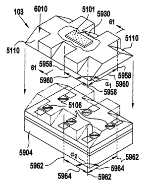
FIG. 59 shows an expanded perspective view of an embodiment of integrated
optical/electronic circuit using flip chip circuits;
FIG. 60 shows a perspective expanded view of an alternate embodiment of
integrated
optical/electronic circuit;
FIG. 61 shows a side cross-sectional view of one embodiment of an
optical/electronic I/O flip chip portion as taken through sectional Iines
61/61 of FIG. 60;
FIG. 62 shows another cross-sectional view as taken through a cross-sectional
lines
61-61 of FIG. 60, in accordance with an alternative embodiment in which a
lower surface is
etched;
FIG. 63, including FIGs. 63A to 63D, shows a method of fabricating the
partially
completed integrated optical/electronic circuit of FIG. 51;
FIG. 64A shows a plot of intensity versus distance from a ledge of one
embodiment
of input/output light coupler 112 including a tapered gap portion;
FIG. 64B shows another plot of intensity at a prism base for another
embodiment of
input/output light coupler having a prism, but without a tapered gap portion;
FIG. 64 shows the integrated optical/electronic circuit of FIG. 51 during a
portion of
the processing;
FIG. 65 shows a perspective view of one embodiment of hybrid active electronic
and
optical circuit that is configured as a J-coupler;
FIG. 66 shows a top view of the hybrid active electronic and optical circuit
of FIG.
65;
FIG. 67 illustrates one embodiment of a mask used to anisotropically etch
regions of
a hybrid active electronic and optical circuit;
2'S FIG. 6~ shows one embodiment of a method of anisotropically etching using
a mask.
9
CA 02449106 2003-12-04
WO 02/093211 PCT/US02/15519
FIG. 69 shows a top view of one embodiment of hybrid active electronic and
optical
circuit that is configured as a two dimensional taper;
FIG. 70 shows a top view of another embodiment of hybrid active electronic and
optical circuit that is configured as a two dimensional taper;
FIG. 71 shows a top view of yet another embodiment of hybrid active electronic
and
optical circuit that is configured as a two dimensional taper;
FIG. 72 shows a top view of an embodiment of hybrid active electronic and
optical
circuit that is configured as an adiabatic taper;
FIG. 73 shows a perspective view of an embodiment of hybrid active electronic
and
optical circuit that is configured as a simple Fabry-Perot cavity;
FIG. 74 shows a perspective view of an embodiment of hybrid active electronic
and
optical circuit that is configured as a coupled Fabry-Perot cavity;
FIG. 75 shows a side view of one embodiment of grating similar to as included
in the
simple Fabry-Perot cavity of FIG. ?3;
FIG. 76 shows a side view of another embodiment of grating from FIG. 75 that
is
configured as a hybrid active electronic and optical circuit;
FIG. 77 shows a side view of yet another embodiment of grating from FIG. 75
that is
configured as a hybrid active electronic and optical circuit;
FIG. 78 shows a top view of another embodiment of hybrid active electronic and
optical circuit that is configured as a wavelength division multiplexer
modulator;
FIG. 79 shows a top view of yet another embodiment of hybrid active electronic
and
optical circuit that is configured as a wavelength division multiplexes
modulator;
FIG. 80 shows a top view of another embodiment of hybrid active electronic and
optical circuit in addition to multiple Echelle gratings and multiple lens
that is configured as
a wavelength division multiplexes modulator;
CA 02449106 2003-12-04
WO 02/093211 PCT/US02/15519
FIG. 81 shows a top view of another embodiment of hybrid active electronic and
optical circuit that is configured as a simple diode; and
FIG. 82 shows a perspective view of one embodiment of prior art photonic band
gap
device;
FIG. 83 shows a perspective view of one embodiment of a photonic band gap
device;
FIG. 84 shows a top view of one embodiment of optical waveguide device;
FIG. 85 shows a top view of another embodiment of photonic band gap device;
FIG. 86 shows a top view of an array of photonic crystals used in a photonic
waveguide device;
FIG. 87 shows a side view of one embodiment of a mufti-level photonic
waveguide
device;
FIG. 88 shows a side view of another embodiment of a photonic waveguide
device;
FIG. 89 shows one embodiment of a computer program used to simulate integrated
optical/electronic circuits;
FIG. 90 shows another embodiment of hybrid active electronic optical circuit
from
that shown in FIG. 81; and
FIG. 91 shows another embodiment of hybrid active electronic optical circuit
from
that shown in FIG. 90.
Detailed Description of the Embodiment
The present disclosure describes many aspects of multiple embodiments of an
integrated optical/electronic circuit 103. This disclosure describes to the
structural features
of the integrated opticallelectronic circuit 103. Different embodiments of the
integrated
optical/electronic circuit include so-called silicon-on-insulator (SOI)
technology, silicon on
sapphire, and other technologies. SOI technology has become prevalent in the
electronics
11
CA 02449106 2003-12-04
WO 02/093211 PCT/US02/15519
industry, and is utilized in such large-production processors as the POWER
PCTM, and such
major companies as IBM and MOTOROLA have devoted considerable research and
development resources to SOI. Certain aspects of the integrated
optical/electronic circuit
103 are described in the "Integrated Optical/Electronic Circuit" portion of
this disclosure.
Another aspect of this disclosure relates to the optical functionality that
may be
provided by the integrated optical/electronic circuit 103. The integrated
optical/electronic
circuit 103 includes a plurality of varied optical waveguide devices 100 (that
may be viewed
as optical building blocks) that together perform the overall opto-electric
functionality of the
integrated optical/electronic circuit 103. One embodiment of the optical
waveguide devices
100 includes a field effect transistor (FET) that is arranged to control the
light flowing
therethrough to perform the various functions.
The most basic function of one of the optical waveguide devices 100 is to act
as an
optical modulator. Other optical waveguide devices 100 may be configured as
active or
passive optical circuits to perform such optical functions as optical
deflection, optical
filtering, optical attenuation, optical focusing, optical path length
adjustment, variable phase
tuning, variable diffraction efficiency, optical coupling, and optical
switching. The structure
of the optical waveguide device 103 is described in the "optical waveguide
device structure"
portion of this disclosure. Certain physics aspects of the optical waveguide
device is
described in the "waveguide physics" portion of this disclosure.
Actual embodiments of discrete optical waveguide devices are described in the
"Specific Embodiments of Optical Waveguide Device" portions of this
disclosure. More
complex optical circuits including a plurality of optical waveguide devices
103 are described
in the "Optical Circuits Including Optical Waveguide Devices" portion of this
disclosure.
Significant aspects of designing any optical waveguide devices 100 include
being
able to couple light from outside of the optical waveguide device to inside of
the waveguide,
12
CA 02449106 2003-12-04
WO 02/093211 PCT/US02/15519
and conversely being able to couple light from the optical waveguide within
the optical
waveguide device to outside of the optical waveguide device. If the coupling
is poor, then
the optical waveguide device will be ineffective since the light cannot be
effectively input
into, or output from, the waveguide. In using relatively thin SOI waveguides,
the options of
coupling techniques are diminished. Certain embodiments of coupling techniques
are
disclosed in the "Input/output Coupling Embodiments" portion of this
disclosure.
Passive optical devices can be made active by the application of an active
electronic
circuit applying a voltage to a metallized or highly conductive, doped
semiconductor portion
proximate the passive optical waveguide, the thereby varying the effective
mode index in
the waveguide by changing the free-carrier concentration. Such devices and
circuits are
described in the hybrid active electronic and optical circuit portion of this
disclosure.
Photonic Band Gap Devices are a promising technology by which such functions
as
modulation, reflection, and diffraction can be performed upon light travelling
within a
waveguide. Shallow photonic band gap devices are considered those devices that
are
IS formed from photonic crystals that do not fully extend through the
waveguide. Certain
aspects of the photonic band gap device, especially to hybrid active
electronic and optical
circuit and other integrated optical/electronics circuits, are described in
the photonic band
gap portion of this disclosure.
I. INTEGRATED OPTICAL/ELECTRIC CIRCUIT
FIG. 1 shows one embodiment of an integrated optical/electric circuit 103.
Multiple
embodi;nents of integrated optical/electric circuit 103 are described herein
as being formed
using SOI devices, etc. The integrated optical/electrie circuit can be
configured with and
combination of active optical, passive optical, active electronics, and
passive components
circuit. SOI technology is highly promising for integrated opticaI/electronic
circuits, and
using relatively thin SOI devices (having an upper silicon Iayer less than 10
~,) has many
13
CA 02449106 2003-12-04
WO 02/093211 PCT/US02/15519
benefits. Using thin SOI devices for waveguides limits the vertical locations
in which light
can diffract, and therefor acts to localize the light to a relatively narrow
waveguide. Thin
SOI devices can be formed using planar lithography techniques including
deposition and
,etching processes.
SOI is a commonly-used, heavily researched, and highly accepted technology fox
electronics using semiconductors. Modifying the already-accepted SOI platform
for optical
circuits instead of developing an entirely new technology makes sense.
Additionally, it is
easier for the SOI engineers and practitioners to extend the SOI technology
compared to
developing, and becoming experienced with, a new technology. Finally, the SOI
simulation
tools have been refined to such a level that the industry trusts the SOI
tools. It is easier to
modify, and use trusted output from, the SOI simulation tools than going
through the effort
and expense of developing new simulation tools. In case of active devices, the
detailed
topology and material profile output from the process simulation and free
carrier
concentration prof 1e output from the device simulator is used to predict the
optical
characteristics of the active device.
II. OPTICAL WAVEGUIDE DEVICE STRUCTURE
There are a variety of optical waveguide devices 100 that are described in
this
disclosure in which light travels within, and is contained within, a
waveguide. Different
embodiments of optical waveguide devices are described that perform different
functions to
the light contained in the waveguide. Altering the shape or structure of an
electrodes) can
modify the function of the optical waveguide device 100. Embodiments of
optical
waveguide devices include a waveguide located in a Field Effect Transistor
(FET) structure
as shown in FIGs. 1 to 3; a waveguide associated with metal oxide
semiconductor capacitor
(MOSCAP) structure is shown in FIG. 4; and a waveguide located in the FIigh
Electron
Mobility Transistor (HEMT) as shown in FIG. 5. Tn MOSCAPs, one or more body
14
CA 02449106 2003-12-04
WO 02/093211 PCT/US02/15519
contacts) is/are separated from the gate electrode by a semiconductor
waveguide and an
electrical insulator. MOSCAPS and MOSFETS and other similar structures are
understood
by the type of dopings in contact with the electrodes; which in turn controls
the electrical
characteristics of the structures. To make the description for the above
embodiments more
uniform,,the term "body contact electrodes" is used to describe either the
body contact at the
base of the MOSCAP or the substantially common potential source electrode and
drain
electrode in the FET-like structure.
The application of the voltage between the gate and body contacts)
predominantly
changes the distribution of free-Garners (either electrons or holes) near the
semiconductor/electrical insulator boundary. These essentially surface
localized changes in
the free Garner distributions are referred to as two-dimensional electron gas
or 2DEG
included in MOSCAPs. In a FET structure, fox example, an increase in the
application of
the bias leads consecutively to accumulation of charges (of the same type as
the
semiconductor i.e. holes in a p-type and electrons in n-type, depletion, and
finally inversion.
In ~DEGs, the polarity of semiconductor is opposite the type of the
predominant free
Garners, i.e. electrons in p-type or holes in n-type). In a High Electron
Mobility Transistor
(HEMT), the electron (hole) distribution formed just below the surface of the
electrical
insulator is referred to as ZDEG because of particularly low scattering rates
of charge
carriers. At any rate, for the purposes of clarity, all of the above shall be
referred to as
2DEG signifying a surface localized charge density change due to application
of an external
bias.
The term "semiconductor" is used through this disclosure in particular
reference to
the waveguides of the particular optical waveguide devices. The semiconductor
waveguide
is intended to represent a class of semiconductor materials. Silicon and
Germanium are
natural single element semiconductors at room temperature. GaAs and InP are
examples of
CA 02449106 2003-12-04
WO 02/093211 PCT/US02/15519
binary compound semiconductors. There are semiconductors made from three
element
semiconductors such as AIGaAs. The salient feature of all semiconductors is
the existence
of a band-gap between the valence and the conduction band. Multiple layers of
semiconductors may also be used in the construction of a waveguide as well as
to create an
optical waveguide device including a MOSCAP, a FET, or a HEMT. For the purpose
of this
disclosure, the semiconductor provides the ability to control the density of
the 2DEG by the
application of the gate voltage. Any description of a specific semiconductor
in this
disclosure is intended to be enabling, exemplary, and not limiting in scope.
The concepts
described herein are intended to apply to semiconductors in general.
These concepts relating to the optical waveguide device apply equally well to
any
mode of light within a waveguide. Therefore, different modes of light can be
modulated
using multi-mode waveguides. The physical phenomena remains as described above
for
mufti-mode waveguides.
The embodiments of optical waveguide device 100 shown in multiple figures
including FIGS. 1-3, and S, etc. include a field effect transistor (FET)
portion 116 that is
electrically coupled to a waveguide 106. One embodiment of the waveguide is
fabricated
proximate to, and underneath, the gate electrode of the FET portion 116. The
waveguide
I06 is typically made from silicon or another one or plurality of III-V
semiconductors. The
FET portion 116 includes a first body contact electrode 118, a gate electrode
120, and a
second body contact electrode 122. A voltage can be applied by e.g., a voltage
source, 202
to one of the electrodes. The gate electrode 120 is the most common electrode
in which the
voltage level is varied to control the optical waveguide device. If the first
body contact
portion 118 and the second body contact portion are held at the same voltage
by placing an
electrical connector 204 there between, then the optical waveguide device 100
operates as a
diode. If there is not electrical connector between the first body contact
portion 118 and the
16
CA 02449106 2003-12-04
WO 02/093211 PCT/US02/15519
second body contact portion 122, then the optical waveguide device 100 acts as
a transistor.
This is true for each of the following FET/diode configurations. Whether any
FET optical
waveguide device 100 is biased to act as a transistor or diode, the optical
waveguide device
100 is within the intended scope of the present invention since either a diode
or a transistor
is capable of altering the effective mode index in the waveguide as described
herein.
The variation in voltage level changes the propagation constant of at least a
portion
of the waveguide ,106. The changes in the index profile of the waveguide are
determined by
the location and shapes of all the electrodes. The density of the 2DEG
generally follows the
shape of the gate electrode I20. Therefore, the shape of the gate electrode
may be
considered as being projected into a region of changeable propagation constant
190 (the
value of the propagation constant may vary at different locations on the
waveguide 106).
The region of changeable propagation constant 190 is considered to be that
region through
the height of the waveguide in which the value of the propagation constant is
changed by
application of voltage to the gate electrode 120. Gate electrodes 120 are
shaped in non-
rectangular shapes (as viewed from above or the side depending on the
embodiment) in the
different embodiments of optical waveguide device. The different embodiments
of the
optical waveguide device perform such differing optical functions as optical
phase/amplitude modulation, optical filtering, optical deflection, optical
dispersion, etc.
Multiple ones of the optical waveguide devices can be integrated into a single
integrated
optical/electronic circuit as an arrayed waveguide (AWG), a dynamic gain
equalizer, and a
large variety of integrated optical/electronic circuits. Such optical
waveguide devices and
integrated optical/electronic circuits can be produced using largely existing
CMOS and other
semiconductor technologies.
FIGs. 1 to 3 will now be described in more detail, and respectively show a
front, top,
2S and side view of one embodiment of an optical waveguide device 100. FIG. 1
shows a
17
CA 02449106 2003-12-04
WO 02/093211 PCT/US02/15519
planar semiconductor waveguide bounded by low-index insulating materials to
which the
light is coupled using a light coupler 112. Other well-known types of coupling
include
gratings, tapers, and butt-coupling that are each coupled to the end of the
waveguide. The
"gate" electrode 120 is positioned directly above the light path in the
semiconductor
S waveguide. The gate electrode is separated from the semiconductor by the low-
index
dielectric acting as an electrical insulator. The body contact electrodes are
electrically
coupled to the semiconductor. This embodiment may be considered to be a FET
structure
with the body contact electrodes 118, 122 forming a symmetric structure
typically referred
to as "source" and "drain" in FET terminology. A substantially constant
potential conductor
204 equalizes the voltage level between the first body contact electrode 118
and the second
body contact electrode 122. The first body contact electrode and the second
body contact
electrode can thus be viewed as providing symmetrical body contact electrodes
to the
semiconductor. In another embodiment, the body contact is placed directly
underneath the
Iight path and underneath the waveguide.
IS In yet another embodiment, the body contact is positioned symmetrically
laterally of
both sides of, and underneath, the incident light path within the waveguide.
The body
contact in each of these embodiments is designed to change a free-carrier
distribution region
in a two dimensional electron gas (2DEG) 108 near the semiconductor/electrical
insulator
boundary of the waveguide along the light travel path. This change in free-
carrier
distribution results from application of the potential between the insulated
gate electrode and
the one or plurality of body contact electrades connected to the body of the
semiconductor.
The FIG. 1 embodiment shows the optical waveguide device 100 including an
integrated field effect transistor (FET) portion 116. The field effect
transistor (FET) portion
116 includes the gate electrode 120, the first body contact electrode 118, and
the second
2S body contact electrode 122, but the channel normally associated with a FET
is either
98
CA 02449106 2003-12-04
WO 02/093211 PCT/US02/15519
replaced by, or considered to be, the waveguide 106. Examples of FETs that can
be used in
their modified form as FET portions 116 (by using the waveguide instead of the
traditional
FET channel) include a metal-oxide-semiconductor FET (MOSFET), a metal-
electrical
insulator-semiconductor FET (MISFET), a metal semiconductor FET (MESFET), a
modulation doped FET (MODFET), a high electron mobility transistor (HEMT), and
other
similar transistors. In addition, a metal-oxide-silicon capacitor (MOSCAP) may
also be
similarly modified to form a FET portion.
FIGS. 1, 2, and 3 shows one embodiment of optical waveguide device 100 that
includes a substrate 102, a first electrical insulator layer 104, a waveguide
106, a first body
contact well 107, a second body contact well 109, the 2DEG 108, a second
electrical
insulator layer 110, an input light coupler 112, an output light coupler 114,
and the field
effect transistor (FET) portion 116. The 2DEG 108 is formed at the junction
between the
silicon waveguide 106 and the second electrical insulator layer 110 of the
waveguide 106.
Multiple embodiments of optical waveguide devices are described that, upon
bias of the gate
electrode 120 relative to the combined first body contact electrode 118 and
second body
contact electrode 122, effect the passage of light through the waveguide 106
to perform a
variety of functions.
The FIG. I2 embodiment of semiconductor waveguide (which may be doped) 106
has a thickness h, and is sandwiched between the first electrical insulator
layer 104 and the
second electrical insulator layer 110. The first electrical insulator layer
104 and the second
elecfirical insulator layer 110 are each typically formed from silicon dioxide
(glass) or any
other electrical insulator commonly used in semiconductors, for example SiN.
The
electrical insulator layers 104, 110 confine the light using total internal
reflection of the light
traversing the waveguide 106.
2S Light is injected into the waveguide 106 via the input light coupler 112
and light
19
CA 02449106 2003-12-04
WO 02/093211 PCT/US02/15519
exits from the waveguide 106 via the output light coupler 114, although any
light-coupling
device can be used to respectively inject or remove the light from the
waveguide 106.
Examples of light-coupling devices include prisms, gratings, tapers, and butt-
couplings.
Light passing from the input light coupler (or other input port) to the output
light coupler (or
other output port) follows optical path 101 as shown in FTG. 1. The optical
path 101 may be
defined based upon the function of the optical waveguide device 100. For
example, if the
optical waveguide device functions as an optical modulator, optical deflector,
or an optical
filter, the optical path 101 can be respectively considered to be an optical
modulation region,
an optical deflection region, or an optical filtering region, etc.
As described earlier, application of voltage on the gate electrode 120
relative to the
combined first body contact electrode 11 ~ and second body contact electrode
122 leads to a
change in the propagation constant via changes induced in the free-carrier
density
distribution 10~. In a MOSCAP, the capacitance of the device is controlled by
the voltage
due to presence (or absence) of 2DEG. In case of a FET, changes in the free
carrier
IS distribution also control the conductance between the first body contact
electrode and the
second body contact electrode. The free-carriers are responsible for changing
the optical
phase or the amplitude of the guided wave depending on their density which in
turn is
controlled by the gate voltage. The basis of field-effect transistor action,
i.e., rapid change
in 2DEG as a function of gate voltage, is also responsible for the control of
the light wave
and enables integration of electronic and optical functions on the same
substrate. Thus
traditional FET electronic concepts can be applied to provide active optical
functionality in
the optical waveguide device 100. The FET portion 116 is physically located
above, and
affixed to, the waveguide 106 using such semiconductor manufacturing
techniques as
epitaxial growth, chemical vapor deposition, physical vapor deposition, etc.
The propagation constant (and therefore the effective mode index) of at least
a
CA 02449106 2003-12-04
WO 02/093211 PCT/US02/15519
portion of the waveguide in the optical waveguide device 100 is changed as the
free carrier
distribution 108 changes. Such changing of the propagation constant results in
phase
modulation of the light passing tbrougl? that device. The phase modulation
occurs in a
regions of changeable propagation constant, indicated in cross-hatching in
FIGs. 1 and 3 as
190, that closely follows the two-dimensional planar shape of the gate
electrode through the
height of the waveguide to form a three dimensional shape.
FIG. 2 shows one embodiment of a voltage source configuration that biases the
voltage of the optical waveguide device 100 by using a voltage source 202 and
a
substantially constant potential conductor 204. The substantially constant
potential
conductor 204 acts to tie the voltage level of the first body contact
electrode 118 to the
voltage level of the second body contact electrode 122. The voltage source 202
biases the
voltage level of the gate electrode 120 relative to the combined voltage level
of the first
body contact electrode 118 and the second body contact electrode 122.
To apply a voltage to the gate electrode, a voltage source 202 applies an AC
voltage
vg from the gate electrode 120 to the combined first body contact electrode
118 and second
body contact electrode 122. The AC voltage vg may be configured either as a
substantially
regular (e.g. sinusoidal) signal or as an irregular signal such as a digital
data transmission.
In one embodiment, the AC voltage vg may be considered as the information
carrying
portion of the signal. The voltage source 202 can also apply a DC bias Vg to
the gate
electrode 120 relative to the combined first body contact electrode 118 and
second body
contact electrode 122. Depending on the instantaneous value of the Yg, the
concentration of
the 2DEG will accumulate, deplete, or invert as shown by the different regions
in FIG. 6. In
one embodiment, the DC bias Vg is the signal that compensates for changes in
device
parameters. The combined DC bias Vg and AC voltage vg equals the total voltage
Y~ applied
to the gate electrode by the voltage source 202. It will be understood from
the description
29
CA 02449106 2003-12-04
WO 02/093211 PCT/US02/15519
above that modulation of vo can thus be used to effect, for example, a
corresponding
modulation of light passing through the waveguide 106.
The voltage potential of the first body contact electrode 118 is tied to the
voltage
potential of the second body contact electrode 122 by the substantially
constant potential
conductor 204. Certain embodiments of the substantially constant potential
conductor 204
include a meter 205 (e.g. a micrometer) to measure the electrical resistance
of the gate
electrode from the first body contact electrode to the second body contact
electrode. The
term "substantially" is used when referring to the constant potential
conductor because the
meter 205 may generate some relatively minor current levels in comparison to
the operating
voltage and current levels applied to the optical waveguide device. The minor
current levels
are used to measure the resistance of the gate electrode. The current level
produced by the
meter is relatively small since the voltage (typically in the microvolt range)
of the meter is
small, and the waveguide resistance is considerable (typically in the tens of
ohms).
The electrical resistance of the gate electrode is a function of such
parameters as gate
voltage, temperature, pressure, device age, and device characteristics. As
such, the voltage
(e.g. the AC voltage or the DC voltage) applied to the gate electrode can be
varied to adjust
the electrical resistance of the gate electrode to compensate for such
parameters as
temperature, pressure, device age, andlor device characteristics. Therefore,
the voltage
applied to the gate electrode can be adjusted to compensate for variations in
the operating
parameters of the optical waveguide device.
As the temperature of the optical waveguide device varies, the DC bias Trg
applied to
the gate electrode 120 of the optical waveguide device is adjusted to
compensate for the
changed temperature. Other parameters (pressure, device age, device
characteristics, etc.)
can be compensated for in a similar manner as described for temperature (e.g,
using a
pressure sensor to sense variations in pressure). This disclosure is not
limited to discussing
22
CA 02449106 2003-12-04
WO 02/093211 PCT/US02/15519
the sensing and compensating for temperature since the other parameters can be
compensated for in a similar manner. Different meter 205 and/or controller 201
embodiments may be provided to compensate for the different temperatures.
FIG. 7 shows an embodiment of method 700 that compensates for temperature
variations in an optical waveguide device. The method 700 starts with step 702
in which the
temperature sensor 240 determines the temperature of the optical waveguide
device. The
temperature sensor 240 can be located either on the substrate or off the
substrate. The
temperature sensor inputs the temperature determined by the temperature sensor
to the
controller 201 in step 703. The method 700 continues to step 704 in which the
DC bias ~g
x0 that is applied to the gate electrode is adjusted to compensate for
variations in the
temperature. The controller 201 includes stored information that indicates the
required
change in DC bias ahgthat is necessary to compensate for variations in
temperature, for
each value of DC bias Yg for each temperature within the operating range of
the optical
waveguide device. The method 700 continues to step 706 in which the AC voltage
vg is
applied to operate the optical waveguide device as desired in the waveguide.
The amount of AC voltage vg is then superimposed on the DC bias Yg that is
applied
to the gate electrode to provide for the desired operation of the optical
waveguide device 200
(e.g. the voltage necessary for optical modulation, optical filtering, optical
focusing, etc.).
The AC voltage vg superimposed on the combined DC bias hg and the DC bias
change dDC
yields the total signal VG applied to the gate electrode.
Another embodiment of compensation circuit, that compensates for the change in
temperature or other operating parameters) of the optical waveguide device,
measures the
electrical resistance of the gate between the first body contact electrode 11~
and the second
body contact 122. The electrical resistance of the waveguide is a function of
temperature,
device age, device characteristics, and other such parameters. The meter 205
measures the
23
CA 02449106 2003-12-04
WO 02/093211 PCT/US02/15519
electrical resistance of the waveguide. For a given waveguide, the same
resistance
corresponds to the same electron density and the same hole density in the
waveguide.
Therefore, if the same electrical resistance of the waveguide is maintained,
the optical
waveguide will behave similarly to cause a similar amount of such optical
action as optical
modulation, optical filtering, optical focusing, or optical deflection.
FIG. 8 shows another method 800 used by the controller 201 to compensate for
temperature variations of the optical waveguide device. The method 800 starts
with step
802 in which the meter 205 measures the electrical resistance of the
waveguide. The
method 800 continues to step 804 in which the measured electrical resistance
of the
waveguide is transferred to the controller 201. The method continues to step
806 in which
the controller applies the amount of DC bias Yg required to be applied to the
gate electrode
for that particular value of electrical resistance of the waveguide. Such
parameters as
temperature and device age that together may change the electric resistance of
the
waveguide can thus be compensated for together. Therefore, after measuring the
electrical
resistance of the waveguide, a feedback loop applies the voltage for that
measured
resistance. The method 800 continues to step 808 in which the AC voltage vg is
applied to
operate the optical waveguide device (i.e. modulate, filter, focus, and/or
deflect light) as
desired in the waveguide.
In both of these temperature compensating embodiments shown in FIGS. 7 and 8,
the
controller 201 allows the DC bias Vg to drift slowly as the temperature varies
to maintain the
average resistance of the waveguide from the source electrode to the drain
electrode
substantially constant. These temperature-compensating embodiments make the
optical
waveguide device exceedingly stable. As such, the required complexity and the
associated
expense to maintain the temperature and other parameters over a wide range of
temperatures
are reduced considerably.
24
CA 02449106 2003-12-04
WO 02/093211 PCT/US02/15519
Suitably changing the voltages applied between the gate electrode 120, and the
combined first body contact electrode 118 and second body contact electrode
122 results in
a corresponding change in the free Garner distribution in the 2DEG 108. In the
FIG. 1
embodiment of optical waveguide device 100, altering the voltage applied to
the gate
electrode 120 of the FET portion 116 changes the density of free carriers in
the 2DEG 108.
Changing free carriers distribution in the 2DEG 108 changes the effective mode
index of the
2DEG 108 in the waveguide. Changing the free Garner distribution similarly
changes the
instantaneous propagation constant level of the region of changeable
propagation constant
190 (e.g., the area generally underneath the gate electrode 120 in the FIG. 1
embodiment)
within the waveguide 106.
Effective mode index, and equivalently propagation constant, both measure the
rate
of travel of light at a particular location within the waveguide taken in the
direction parallel
to the waveguide. For a light beam traveling over some distance in some medium
at a
velocity V, the velocity V divided by the speed of light in vacuum is the
index for that
medium. Glass has a propagation constant of 1.5, which means light travels 1.5
times
slower in glass then it does in a vacuum. For the silicon in the waveguide the
propagation
constant is about 3.5. Since a portion of the light path travels in silicon
and part of the Iight
path is in the glass, the propagation constant is some value between 1.5 and
3.5. Therefore,
the light is travelling at some effective speed measured in a direction
parallel to the axial
direction of the waveguide. That number, or speed, is called effective index
of the
waveguide. Each mode of light has a distinct effective index (referred to as
the effective
mode index) since different modes of the waveguide will effectively travel at
different
speeds.
The effective mode index is the same thing as the propagation constant for any
specific mode of light. The term effective mode index indicates that the
different modes of
CA 02449106 2003-12-04
WO 02/093211 PCT/US02/15519
light within a waveguide travel at different velocities. Therefore there are a
plurality of
effective indexes fox a multi-mode waveguide, each effective index corresponds
to a
different mode of light. The propagation constant (or the effective index)
measures the
average velocity for a phase of light for specific mode travel parallel to the
axis of the
waveguide as shown in FIG. 12. The propagation constant multiplied by the
length would
indicate how long it takes to go that length. Through this disclosure, the
effective index for
a mode (the effective mode index) is considered to be the same measure as the
propagation
constant for that mode of light. The term propagation constant is primarily
used throughout
the remainder of the disclosure for uniformity.
Changing the propagation constant of the waveguide 106 by varying the 2DEG 108
can phase modulate or amplitude modulate the light in the waveguide. Within
the
waveguide, the degree of modulation is local in that it depends on the density
of 2DEG at a
particular location. The shape of the electrode, or other arrangements of body
contact
electrodes, can impose a spatially varying phase or amplitude pattern to the
light beam in the
waveguide. This in turn can be used to accomplish a wide variety of optical
functions such
as variable attenuators, optical programmable filters, switches, etc. on the
optical signals
flowing through the waveguide 106.
A controller 201 controls the level of the total voltage V~ applied to the
voltage
source 202. The optical waveguide device 100 can be employed in a system that
is
controlled by the controller 201, that is preferably processor-based. The
controller 201
includes a programmable central processing unit (CPLI) 230 that is operable
with a memory
232, an input/output (TJO) device 234, and such well-known support circuits
236 as power
supplies, clocks, caches, displays, and the like. The I/O device receives, for
example,
electrical signals corresponding to a desired modulation to be imposed on
light passing
through the waveguide 106. The controller 201 is capable of receiving input
from hardware
26
CA 02449106 2003-12-04
WO 02/093211 PCT/US02/15519
in the form of temperature sensors and/or meters for monitoring parameters
such as
temperature, optical wavelength, light intensity, device characteristics,
pressure, and the
like. All of the above elements are coupled to a control system bus to provide
for
communication between the other elements in the controller 201 and other
external
elements.
The memory 232 contains instructions that the CPU 230 executes to facilitate
the
monitor and control of the optical waveguide device 100. The instructions in
the memory
232 are in the form of program code. The program code may conform to any one
of a
number of different programming languages. For example, the program code can
be written
in G, C++, BASIC, Pascal, or a number of other languages. Additionally, the
controller 201
can be fashioned as an application-specific integrated circuit (ASIC) to
provide for quicker
controller speed. The controller 201 can be attached to the same substrate as
the optical
waveguide device 100.
In the FIG. 1 embodiment of waveguide 106, electrons (hole) concentrate in the
waveguide to form the 2DEG 10~ that forms a very narrow channel near the
boundary of the
silicon waveguide 106 and the second electrical insulator layer 110. The
surface inversion
charge density qn in the 2DEG 1 OS is a direct function of the local surface
potential ~S
applied to the waveguide 106. The local surface potential ~S is, in turn,
directly related to
the total instantaneous voltage on the gate electrode 120. The total voltage
of light in the
waveguide Y~ satisf es the equation Yo = Yg + v~, where Yg is the DC bias and
vg is the AC
bias. The local surface potential ~s is a function of the total voltage Yo,
and is given by the
equations:
~S = Q + VG + Q~X + ~ms
G Cox
27
CA 02449106 2003-12-04
WO 02/093211 PCT/US02/15519
~s = ~ -I- j~G
The total potential Y~ that is applied to the waveguide 106 is thus a factor
of the
effective capacitance C of the optical waveguide device 100. The effective
capacitance C
itself depends on the distribution of the free-carriers. Thus, the capacitance
in the MOB Like
device is a function of the applied voltage. The charges Q and capacitance C
in the equation
1 above are measured per unit area. Since the 2DEG density depends only on ~S,
dopant
density, and temperature; 2DEG density qn can be plotted vs. cps. FIG. 6
illustrates a curve
602 that plots surface charge density as a function of surface potential for
an Si/Si02
MOBCAP where the uniform dopant density is assumed to be 10'6 cm a at room
temperature.
FIG. 6 also shows curve 604 that plots phase shift that is applied to the
optical wave passing
through waveguide i06 for a 3 mm long rectangular gate region. The phase shift
is plotted
as a function of surface potential ~S.
A side view of one embodiment of the optical waveguide device including a
waveguide located in a MOBCAP is shown in FIG. 4. The optical waveguide device
includes a MOBCAP 400 including a body contact 402, a waveguide 106, an
electric
insulator layer 405, and a gate electrode 406. In the embodiment of MOBCAP
similar to as
shown in FIG. 4, a voltage source 410 applies a voltage between the gate
electrode 406 and
the body contact 402 to alter a level of propagation constant in a region of
changeable
propagation constant 190 within the waveguide 106. The variations to the
effective mode
index and the propagation constant result occur similarly to in the FET
embodiments of
optical waveguide device 100 as described below.
In the MOBCAP embodiment of optical waveguide device shown in FIG. 4, the body
contact 402 is positioned below the waveguide 106. Alternatively, body
contacts may be
located where the traditional source and drain electrodes exist on traditional
FETs. The
28
CA 02449106 2003-12-04
WO 02/093211 PCT/US02/15519
body contact in the FET embodiment of optical waveguide device shown in FIGS.
1 to 3 is
formed from the first body contact electrode being electrically coupled at the
same potential
as the second body contact electrode. Application of the electric field due to
the potential
difference between the "gate" and the body contacts results in changes in the
distribution of
free charges as shown in the embodiment of FIG. 4.
FIG. 5 discloses one embodiment of high electron mobility transistor (HEMT)
500.
The HEMT 500 comprises a semi-electric insulating substrate 502, an undoped
buffer
waveguide layer 106, an undoped spacer layer 506, a doped donor layer 508, a
2DEG 505,
the first body contact electrode 118, the gate electrode 120, and the second
body contact
electrode 122. In one embodiment, the semi-insulating substrate 502 is formed
from
AIGaAs. The undoped buffer waveguide layer 106 is formed from Ga.As. The
undoped
spacer layer 506 is formed from AlGaAs. The doped donor layer 508 is formed
from a
doped AIGaAs.
During operation of the optical waveguide device, the 2DEG 505 increases in
height
(taken vertically in FIG. 5) to -approximately 20 angstroms. The 2DEG 505 is
generated at
the interface between the undoped spacer layer 506 and the undoped buffer
waveguide layer
106 as a result of the negative biasing of the doped donor layer 508. Such
negative biasing
drives the electron carriers in a 2DEG 505 generally downward, thereby forming
a p-type
2DEG 505. Application of voltage to the gate electrode tends to increase the
free carrier
distribution in those portions of the 2DEG 505 that are proximate the gate
electrode. Such
an increase in the free carrier distribution in the 2DEG increases the
effective mode index in
the waveguide 106 formed underneath the 2DEG 505. The gate electrode 120 is
formed
having a prescribed electrode shape. The shape of the effective mode index
region within
the waveguide 106 (i.e., the region having an effective mode index that is
changed by the
application of voltage to the gate electrode) generally mirrors the shape of
the gate electrode
29
CA 02449106 2003-12-04
WO 02/093211 PCT/US02/15519
120 as viewed from above in FIG. 5. Additionally, the undoped spacer layer 506
acts as an
insulative layer, to allow the formation of the 2DEG. HEMTs are formed in a
variety of
embodiments, several of which are described in U.S. Patent No. 6,177,685 to
Teraguchi et
al. that issued on January 23, 2001 (incorporated herein by reference in its
entirety).
From semiconductor physics, the change in the distribution of free charges is
most
pronounced near the electrical insulator-semiconductor boundary. These changes
in the
free-carrier distribution change the index profile of the optical waveguide
from a well-
known relationship in plasma physics given by the Drude Model. The change in
the free
carrier distribution changes the propagation constant of the optical waveguide
device from a
well-known relationship in plasma physics given by the Drude model in a region
of
changeable propagation constant 190 within the waveguide. The changes in the
free-earner
distribution induced in the semiconductor by the application of electric
fields between the
gate electrode and the body contact electrodes) modulates the phase andlor
amplitude of the
optical wave passing through the region of changeable propagation constant
190. Thus,
ZS local changes in the free carrier distribution induced by a change in
applied voltage to the
gate electrode are impressed on fihe local optical phase or the amplitude of
light passing
through the waveguide. The shape of the charge distribution, i.e., the region
of changeable
propagation constant 190, provides the appropriate optical function as
described below. In
multiple embodiments, the pattern of the gate electrode (i.e., the planar
shape of the .gate)
controls the shape of the free earner distribution. The change in free carrier
distribution, in
turn, changes the local effective mode index, or propagation constant, of the
waveguide in
the region of changeable propagation constant 190. The same phenomena of
change in the
refractive index profile of the waveguide may be ascribed by indicating that
group delay or
the group velocity of the light beam has been changed as the free carrier
distribution varies.
Therefore, the effective mode index, the propagation constant, the group
delay, or
CA 02449106 2003-12-04
WO 02/093211 PCT/US02/15519
the group velocity relate to an equivalent concept, namely, parametizing
changes in the
waveguide's refractive index profile on the optical beam passing through the
region of
changeable propagation constant 190 in the waveguide. This principle applies
to all
embodiments of optical waveguide devices, including those shown in FIGS. 1-3,
4, and S.
The relationship between the effective mode index, the propagation constant,
the
group delay, or the group velocity apply to waveguides of all thickness' is
now considered.
In the case of "thick" waveguides, the light ray travels by bouncing between
the two
bounding planes defined by the insulator layers 110 and 104. The light ray can
be easily
identified, typically using the concept of phase or amplitude changes that are
directly
imposed on a beam that has directly undergone one or multiple interactions
with free
carriers. However, the concepts of effective mode index, propagation constant,
group delay,
or group velocity signify the same final result on the light beam. In this
disclosure, the
terms propagation constant, effective mode index, group delay, and group
velocity are each
used to describe the effects of changes in the free-carrier distribution due
to electric field
applied to a semiconductor in an optical waveguide device, whether the optical
waveguide
device uses FET, HEMT, MOSCAP,. or any other type of optical waveguide device
technology.
Controlling the ZDEG density provides the optical function of an optical
waveguide
device. As described, adjusting the gate voltage can control the 2DEG density.
The.density
may be spatially varied to provide more complex functions. A triangular shaped
density
distribution (included in a region of changeable propagation constant) is
capable of
deflecting the light beam in a fashion similar to a prism in ordinary optics.
An undulating
pattern of 2DEG of a particular spatial period can reflect/deflect a specific
wavelength to
form a grating. The exact shape or the spatial density of the 2DEG is affected
by placement
2~ of body contact electrodes relative to the gate electrode, the shape of the
body contact
31
CA 02449106 2003-12-04
WO 02/093211 PCT/US02/15519
electrodes and the gate electrode, and the applied voltages discussed herein.
The electric
field density between the gate electrode and the body contact electrode
determines the shape
of the 2DEG density. The properties or thickness of the insulator can be
changed to affect
the density distribution. For example, a grating may be constructed by
patterning the gate
electrode as a series of grooves having a constant spacing. In alternate
embodiments, the
gate electrode can have a consistent thickness, but the insulator thickness or
shape can be
altered to change the electrical resistance between the gate electrode and the
waveguide. All
of these embodiments provide an electrically switchable grating by controlling
the 2DEG
density. The 2DEG density pattern follows the surface potential at the
waveguide/electric
insulator boundary rather than the exact shape of the gate electrode.
FIG. 9 shows a top view of another embodiment of optical waveguide device 100
that is similar to that shown in the embodiment of FIG. 2, except that the
optical waveguide
device includes an additional bank gate electrode 902 that is connected to a
bank gate
electrode well 904. The doping charge of the bank gate electrode well 904
(p++) in one
IS embodiment is opposite the doping charge (n++) of the source electrode well
and the drain
electrode well. During operation, a voltage may be applied between the bank
gate electrode
902 and the connected source electrode and drain electrode to establish a
propagation
constant gradient formed within the region of changeable propagation constant
across the
waveguide from the source electrode to the drain electrode. A variety of
alternative
embodiments may be provided to establish a propagation constant gradient
formed within
the region of changed propagation constant across the waveguide. For example
the width of
the second electrical insulator layer 110, or the resistance of the material
used in the second
electrical insulator layer 110 may be varied to establish a propagation
constant gradient
across the waveguide. Since there are such a variety ofFET, MOSCAP, HEMT, and
other
configurations, it is envisioned that those configurations are within the
intended scope of
32
CA 02449106 2003-12-04
WO 02/093211 PCT/US02/15519
optical waveguide device of the present invention.
Optical waveguide devices may be configured either as slab waveguides or
channel
waveguides. In channel waveguides, the guided light is bound in two directions
(x and y)
and is free to propagate in the axial direction. In slab waveguides, the
guided light is bound
in one direction and can propagate freely in two orthogonal directions.
Channel waveguides
are used in such applications as transmission, resonators, modulators, lasers,
and certain
filters or gratings where the guided light is bound in two directions. Slab
waveguides are
used in such applications as deflectors, couplers, demultiplexers, and such
filters or gratings
where the guided light is bound only in one direction, and it may be desired
to change the
direction of propagation.
There are several embodiments of channel waveguides including the FIG. 10
embodiment of the ridge channel waveguides 1000 and the~FIG. 11 embodiment
trench
channel waveguide 1100. The ridge channel waveguide 1000 includes a raised
central
substrate portion 1002, a electrical insulator layer 1004, and a metal gate
electrode 1005.
The raised substrate portion 1002 is n-doped more heavily than the main
substrate 102. The
raised substrate portion 1002 forms a channel defined by a pair of side walls
1006, 1008 on
the sides; the electrical insulator layer 1004 on the top and the n-doping
differential between
the raised substrate portion 1002 and the main substrate I02 on the bottom.
The pair of side
walls 1006, 1008 includes, or is coated with, a material having a similar
index of refraction
as the electrical insulator layers 104. Biasing the metal gate electrode 1005
forms a 2DEG
108 adjacent the electrical insulator layer 1004. The 2DEG 108 allows the
carriers to pass
between the first body contact well 107 and the second body contact well 109
as applied,
respectively, by the respective first body contact electrode 118 and the
second body contact
electrode 122.
FIG. 11 shows one embodiment of trench channel waveguide 1 I00. The trench
33
CA 02449106 2003-12-04
WO 02/093211 PCT/US02/15519
channel waveguide includes a plurality of electrical insulative blocks 1102,
1104 and the
waveguide 106. The electrical insulative block 1102 partially extends into the
waveguide
106 (from the upper surface of the optical waveguide device 100) at a lateral
location
between the first body contact well 107 and the gate electrode I20. The
electrical insulative
block 1104 partially extends into the waveguide 106 (from the upper surface of
the optical
waveguide device 100) at a lateral location between the second body contact
well I09 and
the gate electrode I20. The light passing through the waveguide 106 is
restrained from
travelling laterally by the addition of the electrical insulative blocks 1102,
1104. Spaces
1112, 1114 are defined within the waveguide between each one of the respective
insulative
blocks 1102, 1104 and the first electrical. insulator layer 104. These spaces
allow carriers to
flow between the respective first body contact well 107 and the second body
contact well
109 through the waveguide 106 formed under the gate electrode 120.
One embodiment of the optical waveguide devices 100 can be constructed on so
called silicon on insulator (SOI) technology that is used in the semiconductor
electronics
field. SOI technology is based on the understanding that the vast majority of
electronic
transistor action in SOI transistors occurs on the top few microns of the
silicon. The silicon
below the top few microns, in principal, could be formed from some electrical
insulator such
as glass. The SOI technology is based on providing a perfect silicon wafer
formed on a
layer of an electrical insulator such as glass (silicon dioxide), that starts
two to five microns
below the upper surface of the silicon. The electrical insulator electrically
isolates the upper
two to five microns of silicon from the rest of the silicon.
The inclusion of the electrical insulator in SOI devices limit the large
number of
electric paths that can be created through a thicker silicon, thereby
automatically making
SOI transistors go faster and use less power consumption. SOT technology has
developed
over the past decade to be commercially competitive. For example, Power PC (a
registered
34
CA 02449106 2003-12-04
WO 02/093211 PCT/US02/15519
trademark of Apple Computer, Inc, of Cupertino, CA) has moved to SOI
technology.
The embodiment of optical waveguide device 100 shown, for example, in FTGs. 1
to
3 may be configured using SOI technology such as processors and chips. The
waveguide
106 of the optical waveguide device 100 may be fashioned as the upper SOI
silicon layer.
The first electrical insulator layer 104 may be fashioned as the SOT insulator
layer. The
substrate 102 may be fashioned as the SOI silicon substrate. As such, the SOI
technology
including the majority of processors and chips, can easily be used as an
optical waveguide
device.
IIT. WAVEGITIDE PHYSICS
This section demonstrates that the propagation constant (or equivalently the
effective
mode index) of the waveguide is an instantaneous function of the 2DEG charge
density q".
An increase in the free carrier distribution in a region of the 2DEG l OS
results in a
corresponding increase in the propagation constant of the waveguide 106 at the
corresponding region. The relationship between the volumetric density of the
free carriers
and the refractive index was originally derived by Drude in his Model of
Metals that
indicates that metals provide both a dielectric and "free electron" response.
The same model
may be applied to semiconductors. The changes in the real part of the
refractive index dh
and the imaginary part of the refractive index dk (the imaginary part
corresponds to
absorption) from an increase in the free Garner distribution are a function of
the change in
the free-carrier density dN, as indicated by the following equations:
~n = ~ z HIV = ~t1 N
2~omenw
~k = 0n
~zs
where a is the electronic charge, me is the effective mass of the Garner, z is
the mean
CA 02449106 2003-12-04
WO 02/093211 PCT/US02/15519
scattering time and is related to the mobility, and ~1V is the change in the
free-carrier
density. For the semiconductor devices considered here, where the dominant
change in the
free-carriers is due to the 2DEG, dNis a function of q" and the thiclaiess (t)
of the 2DEG
varies according to the equation:
, DN _- ~q" 4
t2DEG
TABLE 1 shows the calculated values of the Drude coefficient x and the
effective
mass me for Silicon with n or p-type dopants, and Gallium Arsinide (GaAs) with
n-type
doping (at wavelengths of 1.3 and 1.55 micron). GaAs and InP both have a
larger Drude
Coefficient x than silicon. This is in part due to the smaller effective mass
of charge
(electron or hole). Thus, a waveguide structure made from GaAs and InP will
have larger
changes in the propagation constant for the same changes in the density of
2DEG when
compaxed to Silicon.
TABLE 1
WavelengthMaterial x me
1.33 Silicon-n-7x10'zz 0.33
I .55 -9.4x
I 0'zz
I.33 Silicon-p-4x10'zz 0.56
1.55 -S.SxlO'zz
1.33 GaAs-n -3.Sx10'z'0.068
1.55 -4.8x10'z'
1S ~ To estimate the length requirements for a dielectric slab waveguide, the
modes of the
FIG. 12 embodiment of dielectric slab waveguide 106 formed between the
cladding layers
have to satisfy the equation:
36
CA 02449106 2003-12-04
WO 02/093211 PCT/US02/15519
2kyh + ~, + ~z = 2nzTc
where h is the thickness of the waveguide 2 06, and the phase shifts ~, and ~z
are due
to the reflection of the light at the boundary and m is an integer multiple.
The propagation
constant kZ and ky are related to k and the mode angle 0 by the following
equations:
ky = k cos B
kZ = k sin B, and 6
k=C~)
Solving equations 5 and 6 can derive the modes of the waveguide 106. The
values
of ~, and ~z are functions of angle 8. The change in the propagation constant
kz due to
change in the waveguide index profile induced by the 2DEG is responsible for
amplitude
and phase modulation. The phase modulation of the light in the waveguide
results from a
change in the propagation constant of selected regions within the waveguide.
The amplitude
modulation of the light passing through the waveguide results from a change in
the
absorption of the light passing through selected regions within the waveguide.
The shape and type of the material through which light is passing plays an
important
role in determining the optical function of the optical waveguide device. For
example, light
passing through a rectangular slab optical waveguide device only travels
axially along the
optical path 101. Optical deflectors, for example, not only allow the light to
travel axially,
but can also deviate the light laterally. The amount of displacement and
deviation of the
light passing through the waveguide are both dependent on the propagation
constant of the
waveguide as well as the apex angle of the light coupler.
The shape of a region of changeable propagation constant 190 within a
waveguide
plays a role in determining how an application of voltage to the gate
electrode will modify
37
CA 02449106 2003-12-04
WO 02/093211 PCT/US02/15519
the optical characteristics of light passing through the waveguide. For
example, a suitably-
biased prism-shaped gate electrode projects a three dimensional prism-shaped
region of
changeable propagation constant 19D into the waveguide. The cross-sectional
height of the
region of changeable propagation constant 190 is projected through the entire
height of the
waveguide. As viewed from above, the region of changeable propagation constant
190
deflects light in similar propagation directions as light passing through a
similarly shaped
optical Iight coupler. Tn slab waveguides, the rays of light will deflect or
bounce between
the upper and lower surface of the waveguide while continuing in the same
propagation
direction as viewed from above.
Unlike actual optical circuits that are physically inserted in a path of
light, any
effects on Iight passing through the waveguide of the present invention due to
the
propagation constant within a region of changeable propagation constant 190
can be
adjusted or eliminated by altering the voltage level applied to the gate
electrode. For
eacample, reducing the voltage applied to a deflector-shaped gate electrode
sufficiently
results in the propagation constant of the projected deflector-shaped region
of changeable
propagation constant 190 being reduced to the propagation constant value of
the volume
surrounding the region of changeable propagation constant 190. In effect, the
region of
changeable propagation constant i90 will be removed. Light travelling through
the region
of changeable propagation constant 190 will therefore not be effected by the
region of
changeable propagation constant 190 within the waveguide. Similarly, the
strength of the
propagation constant can be changed or reversed by varying the voltage applied
to the gate
electrode.
IV. SPECIFIC EMBODIMENTS OF OPTICAL WAVEGUIDE DEVICES
A variety of embodiments of optical waveguide devices are now described. Each
optical waveguide device shares the basic structure and operation of the
embodiments of
38
CA 02449106 2003-12-04
WO 02/093211 PCT/US02/15519
optical waveguide device described relative to FIGs. 1-3, 4, or 5. The optical
waveguide
device can be configured in either the channel waveguide or slab waveguide
configuration.
Each embodiment of optical waveguide device is an active device, and
therefore, the voltage
level applied to the electrode can control the degree that the light within
the region of
changeable propagation constant 190 in the waveguide will be affected. Since
the optical
waveguide device is active, the propagation constant in the region of
changeable
propagation constant 190 can be adjusted by varying the voltage applied to the
gate
electrode. Allowing for such adjustment using the controller 201 in
combination with either
the meter 20S or the temperature sensor 240 using the methods shown in FIGS. 7
or 8 is
highly desirable considering the variation effects that temperature, device
age, pressure, etc.
have on the optical characteristics of the optical waveguide device.
The embodiments of optical waveguide device 100 described relative to FIGS. 1
to 3,
4, and 5 can be modified to provide a considerable variation in its operation.
For example,
the optical waveguide device 100 can have a projected region of changeable
propagation
constant 190 within the waveguide to provide one or more of phase and/or
amplitude
modulation, optical deflection, optical filtering, optical attenuation,
optical focusing, optical
path length adjustment, variable phase tuning, variable diffraction
efficiency, optical
coupling, etc. As such, embodiments of many optical waveguide devices that
perform
different operations are described in the following sections along with the
operations that
they perform.
In each of the following embodiments of an optical waveguide device, the gate
electrode is formed in a prescribed electrode shape to perform a desired
optical operation.
The projected region of changeable propagation constant 190 assumes a shape
similar to, but
not necessarily identical to, the gate electrode. The shape of the region of
changeable
propagation constant 190 within the waveguide can physically map extremely
closely to,
39
CA 02449106 2003-12-04
WO 02/093211 PCT/US02/15519
with a resolution of down to 10 nm, the prescribed gate electrode shape. The
construction
and operation of different embodiments of optical waveguide devices, and the
operation, and
effects of various embodiments of regions of changeable propagation constant
I90 are
described in this section.
4A. Optical Modulator
This section describes an optical modulator, one embodiment of optical
waveguide
device 100 that modulates light passing through the waveguide. The embodiments
of
optical waveguide device as shown in FIGs. 1-3, 4, or 5 can perform either
phase
modulation or amplitude modulation of light passing through the waveguide. The
modulation of light by the optical waveguide device 100 can be optimized by
reducing the
losses in the gate electrode I20 as well as reducing the charges in the 2DEG
108, while
increasing the interaction of the waveguide mode with the 2DEG. In general,
reducing the
waveguide thickness h reduces the necessary waveguide length LN to produce
modulation.
Limiting the modulation of the 2DEG 108 also limits the effects on the free-
carriers
resulting from absorption during modulation. The length required for a
specific loss, such as
a 10 dB loss LIOdB~ c~ be experimentally determined for each device. Both LN
and L,o~B are
functions of Oqn. Oqn depends on both the DC bias Tag as well peals-to-peak
variation of the
varying AC signal vg
To construct a high-speed modulator operating with bandwidth in excess of, for
example 50 GHz, it is important to consider both the RF microwave interfaces
and the
transit time of the free-carriers. Since the carriers arrive in the 2DEG
either from the bulk
electrode (not shown), from the first body contact electrode I I8, or from the
second body
contact electrode 122, as the voltage of the gate electrode 122 is changed,
the time required
for the voltage to equilibrate to supply a constant voltage is,
4o
CA 02449106 2003-12-04
WO 02/093211 PCT/US02/15519
~ - (L l2~
a
Vs
where vs is the maximum velocity of the corners and L is the channel length
illustrated in FIG. 1. Thus, the maximum length L of the MOS/HEMT structure of
the
optical waveguide device 100 is determined by the requirement that ie be Iess
than some
percentage of the bit period.
FIG. 6 shows an illustrative graph of-the surface charge density and the phase
shift,
both plotted as a function of the surface potential far a planar dielectric
waveguide. In the
FIG. 6 plot, the waveguide is an exemplary planar Si waveguide that has an
electrical
insulator layer such as cladding on both the upper and lower surfaces. The
waveguide is a
single mode waveguide with the propagation constant of 14.300964 ~rri'. A
change in the
gate voltage by approximately 0.2 - 0.5 V results in a change to the surface
charge density
of the 2DEG by 8 x 10'Z cxri Z which in turn will lead to a change of -0.01 in
the propagation
constant if the 2DEG was due to electrons. Further assume that this 2DEG
region is
effectively confined to within 5-50 nm adjacent the upper electrical insulator
layer, as is
typical for MOS device physics. Assuming that there is an index change aver
only a 10 nm
distance, the new propagation constant is calculated to be 14.299792 ~,ni'.
The changes in
the propagation constant result in an additional phase shift of 180 degrees
for light travelling
a length of 2.86 mm. Thus, gate voltage modulation leads to phase modulation
of light in
the waveguide. Similarly, free-corner absorption occurs in the semiconductor
locations
where there are scattering centers (i.e. donor sites). Such free-carrier
absorption acts to
modulate the amplitude of the propagating mode of light. In general, amplitude
modulation
and phase shift modulation will occur simultaneously, but one type of
modulation can be
arranged to be predominant by controlling the doping profile of the waveguide.
In one embodiment, a channel waveguide is used to construct a high-speed
47
CA 02449106 2003-12-04
WO 02/093211 PCT/US02/15519
modulator. With total internal reflection (TIR) using a channel waveguide, all
the light
within the waveguide is constrained to follow the direction parallel to the
optical path 101
since the light that contacts the electrical insulator layers 104, 110 of the
waveguide reflects
off the electrical insulator layers. Electrical insulator layers 104, 110 have
a lower refractive
index than the waveguide. The channel waveguide should be dimensioned to match
the
models) of the waveguide so the waveguide acts as a modulator for that mode.
The first body contact well 107 and the second body contact well 109, that
respectively interact with the first body contact electrode 118 and the second
body contact
electrode 122, are both typically n-doped. This doping produces the body
contact wells 107,
109 having a lower refractive index than the silicon waveguide 106 due to the
presence of
free-carriers. The body contact wells 107, 109 thus form a low-refractive
index cladding
that naturally confine the light models) laterally within the waveguide 106.
The body
contact wells 107, 109 also absorb some light passing through the waveguide
106, but the
absorption of light makes the waveguide lossy. Thus, it may be desired to use
other
refractive elements than the electrodes 118, 122 to confine the travel ofthe
optical modes
and limit the loss of the light.
For high speed modulation, the body contacts and the gate electrodes can be
made to
act like a waveguide that operates at radio frequencies. It is preferred,
depending on the
distance required, to produce the required modulation to match the group
velocity of the
optical wave to the microwave.
Variable optical attenuators are one additional embodiment of optical
amplitude
modulators. The' description of constructing one embodiment of variable
optical attenuator
using optical waveguide devices is described later following a description of
gratings.
4B. Optical Deflectors
42
CA 02449106 2003-12-04
WO 02/093211 PCT/US02/15519
. The FIG. 13 embodiment of the optical waveguide device 100 is capable of
acting as
an optical deflector 1300 to controllably deflect light passing through the
waveguide. In one
embodiment of deflector 1300, the gate electrode 120 shown in the embodiments
of FIGs. 1-
3, 4, and 5 is physically and operationally divided into two electrodes
including the input
light coupler gate electrode 1304 and the output light coupler gate electrode
1306. Both the
input light coupler gate electrode 1304 and the output light coupler gate
electrode 1306 may
be shaped in a trapezoidal or other prismatic) configuration, and are both
substantially co-
planar and physically positioned above the waveguide. When voltage of a first
polarity is
applied to one of the input light coupler gate electrode 1304 or the output
light coupler gate
electrode 1306 (not simultaneously), light will be deflected from the incident
axial direction
of propagation into opposite lateral directions, e.g. respectively downwardly
and upwardly
within the waveguide of FIG. 13. When a voltage of one polarity is applied to
one of the
input light coupler gate electrode 1304, light will be deflected in the
opposite lateral
directions (upward or downward as shown in FIG. 13) as when voltage of the
same polarity
1S is applied to the output light coupler gate electrode 1306.
The input light coupler gate electrode 1304 and the output light coupler. gate
electrode 1306 are both formed from an electrically conductive material such
as metal. A
first voltage supply 1320 extends between the combined first body contact
electrode 118 and
the input light coupler gate electrode 1304. A second voltage supply 1322
extends between
the combined first body contact electrode 118 and second body contact
electrode 122 to the
output light coupler gate electrode 1306. The first voltage supply 1320 and
the second
voltage supply 1322 are individually controlled by the controller 201, and
therefore an
opposite, or the same, or only one, or neither, polarity voltage can be
applied to the input
light coupler gate electrode 1304 and the output light coupler gate electrode
1306. The input
light coupler gate electrode 1304 and the output light coupler gate electrode
1306 can be
43
CA 02449106 2003-12-04
WO 02/093211 PCT/US02/15519
individually actuated so that each one of the deflecting prism gate electrodes
1304, 1306 can
project a region of changeable propagation constant 190 in the waveguide while
the other
deflecting prism gate electrode does not. FIGs. 14 and 15 (including FIGS. I
SA to 15D)
show a shape of an embodiment of first region of changeable propagation
constant 190a
projected by the input light coupler gate electrode 1304 closely maps that
shape of the input
Iight coupler gate electrode shown in FIG. 13. The shape of the FIGs. 14 and
15 (including
FIGS. 15A to 15D) embodiment of second region of changeable propagation
constant I90b
projected by the output light coupler gate electrode 1306 that closely maps
that shape of the
output light coupler gate electrode 1306 shown in FIG. 13.
The input light coupler gate electrode 1304 has an angled surface 1308 whose
contour is defined by apex angle 1312. The output light coupler gate electrode
1306 has an
angled surface 1310 whose contour is defined by apex angle 1314. Increasing
the voltage
applied to either the input light coupler gate electrode 1304 or the output
light coupler gate
electrode 1306 increases the free carrier distribution in the region of the
2DEG adjacent the
respective first region of changeable level of region of changeable
propagation constant
190a or the second region of changeable propagation constant 190b of the
waveguide,
shown in the embodiment of FIG. 15 (that includes FIG. 15A to 1 SD). Both
regions of
changeable propagation constants 190a, 190b are prism (trapezoid) shaped and
extend for
the entire height of the waveguide and can be viewed as.horizontally oriented
planar prisms
located in the waveguide whose shape in the plane parallel to the gate
electrode is projected
by the respective deflecting prism gate electrodes 1304, 1306. The waveguide
volume
within either one of the regions of changeable propagation constant 190a, 190b
has a raised
propagation constant compared to those waveguide regions outside the region of
changeable
propagation constant 190a, 190b. Additionally, a boundary is formed between
each one of
the regions of changeable propagation constant 190x, 190b and the remainder of
the
44
CA 02449106 2003-12-04
WO 02/093211 PCT/US02/15519
waveguide. The fact that each one of the regions of changeable propagation
constant 190a,
190b has both a raised propagation constant level and a boundary makes the
prism-shaped
regions of changeable propagation constant 190a, 190b act as, and indeed be
functionally
equivalent to, optical prisms formed of either semiconductor material or
glass.
S As shown in FIG. 15A, when a level of voltage that is insufficient to alter
the carrier
concentration is applied to either gate electrode 1304 and 1306, no 2DEG 108
is established
between the electric insulator Iayer 110 and the waveguide I06. Since the 2DEG
changes
the level of propagation constant in the respective regions of propagation
constant 190a,
190b, no regions of changeable propagation constants 190a or I90b are
established in the
waveguide 10b. Therefore, the propagation constant of the first region of
changeable
propagation constant 190a in the waveguide matches the propagation constant
level of the
remainder of the waveguide 106, and light travelling along paths 1420, 1422
continues to
follow their incident direction. Path 1420 is shown with a wavefront 1440
while path 1422
is shown with a wavefront 1442.
When voltage of a first polarity is applied to the input light coupler gate
electrode
1304, the first region of changeable propagation constant I90a is projected in
the shape of
the input light coupler gate electrode 1304 through the height of the
waveguide to form the
region of changed propagation constant 190a, as shown in FIG. 15B. The first
region of
changeable propagation constant 190a thus functions as a variable optical
prism that can be
selectively turned on and off. The first region of changeable propagation
constant 190a is
formed in the semiconductor waveguide that deflects the light passing along
the waveguide
along a path 1430 including wavefronts 1432. Individual beams of the light
following path
1430 are reflected with total internal reflectance between an upper and lower
surface of the
waveguide, but the direction of travel of light within the waveguides remains
along the path
2S 1430.
CA 02449106 2003-12-04
WO 02/093211 PCT/US02/15519
The intensity of the voltage applied to the input light coupler gate electrode
1304 can
be reduced to limit the propagation constant level of the region of changed
propagation
constant, so the light following path 1420 would be deflected, e.g., along
path 1436 instead
of along path 1430. The polarity of the voltage applied to the input light
coupler gate
electrode 1304 can also be reversed, and light following path 1420 along the
waveguide
would be deflected to follow path 143. Therefore, the deflection of the light
within the
waveguide 106 can be controlled, and even reversed, by controlling the voltage
applied to
the input light coupler gate electrode 1304. Changing of the propagation
constant within the
first region of changeable propagation constant 190a causes such deflection by
the input
light coupler gate electrode 1304.
When no voltage is applied to the output light coupler gate electrode 1306 as
shown
in FIGS. 15A and 15B, thereby effectively removing the second region of
changeable
propagation constant 190b from the waveguide 106. Light following within
waveguide 106
along path 1422 is assumed to continue in a direction aligned with the
incident light, or in a
1S direction deflected by the input light coupler gate electrode 1304, since
the propagation
constant is uniform throughout the waveguide.
When voltage of a first polarity is applied to the output light coupler gate
electrode
1306, the second region of changeable propagation constant 190b having a
changed
propagation constant level is projected in the waveguide as shown in FIGS. 15C
and 15D.
The second region of changeable propagation constant 190b may be viewed as an
optical
prism that projects in the shape of output light coupler gate electrode 1306
to the waveguide,
thereby deflecting the light passing along the waveguide along path 1460 with
the
wavefronts 1462 extending perpendicular to the direction of travel.
The intensity of the voltage applied to the output light coupler gate
electrode 13D6
2S shown in FIG. 15C can be reduced, so the light following path 1422 would be
deflected at a
46
CA 02449106 2003-12-04
WO 02/093211 PCT/US02/15519
lesser angle, e.g., along path 1466 instead of along path I460. Similarly,
increasing the
voltage applied to the output light coupler gate electrode 1306 increases the
angle of
deflection. The polarity of the voltage applied to the output light coupler
gate electrode
1306 could also be reversed, and light following path 1420 within the
waveguide would be
deflected in a reversed direction to the original polarity to follow path
1468. Therefore, the
deflection of the Light within the waveguide I06 can be controlled, and even
reversed, by
controlling the voltage applied to the output light coupler gate electrode
1306. Additionally,
the propagation constant in prescribed regions of the waveguide, and the gate
resistance, can
be calibrated using the techniques described in FIGS. 7 and 8 using the
controller 201, the
meter 205, and/or the temperature sensor 240.
The voltage being used to bias the input light coupler gate electrode 1304
and/or the
output light coupler gate electrode 1306 have the effect of controllably
deflecting the light as
desired. The FIG. 14 embodiment of optical waveguide device 100 is
structurally very
similar to the FIGs. I to 3 embodiment of optical waveguide device I00,
however, the two
embodiments of optical waveguide devices perform the differing functions of
modulation
and deflection.
In the FIG. 16 embodiment of optical waveguide device, the incident light
flowing
through the waveguide will be deflected from its incident direction in a
direction that is
parallel to the axis of the optical waveguide device. Such deflection occurs
as result of
variable voltage applied between the second body contact electrode 122 and the
first body
contact electrode 118. In this configuration, an additional voltage source
1670 applies a
voltage between the second body contact electrode and the first body contact
electrode to
provide voltage gradient across the gate electrode. By varying the voltage
between the
second body contact electrode and the first body contact electrode, the level
of propagation
constant within the region of changeable propagation constant changes. The
voltage level
47
CA 02449106 2003-12-04
WO 02/093211 PCT/US02/15519
applied to the waveguide thus causes a direction of the propagation of light
flowing through
the waveguide to be controllably changed, leading to deflection of light
within the horizontal
plane (e.g. upward and downward along respective paths 1672, 1674 as shown in
FIG. 16).
The application of the first body contact-to-second body contact voltage T~sD
1670 by
the voltage source causes a propagation constant gradient to be established
across the 2DEG
in the waveguide 106 from the first body contact electrode to the second body
contact
electrode. Thus, the propagation constant, or the effective mode index, of the
waveguide
106, varies. This variation in the propagation constant leads to angled phase
fronts from one
lateral side of the waveguide to another. That is, the wavefront of the
optical light flowing
through the FIG. 1 b embodiment of waveguide on one lateral side of the
wavefront lags the
wavefront on the other lateral side. The phase fronts of the light emerging
from the gate
region will thus be tilted and the emerging beam will be deflected by an angle
y. For a fixed
hDS, the deflection angle y increases with the distance z traveled within the
waveguide. The
angle y can be calculated by referring to FIG. 16 according to the equation.
y = a tan ~4P = a tan ~ ~ ~ - a tan h cot(B)0 Bl~
L . L
.._ ~,=~~~10_4
Another embodiment of optical deflector 1700 is shown in FIG. 17. The
waveguide
1702 is trapezoidal in shape. A gate electrode 1706 (that is shown as hatched
to indicate
that the gate electrode shares the shape of the waveguide 1702 in this
embodiment) may, or
may not, approximate the trapezoidal shape of the waveguide. Providing a
trapezoidal
shaped waveguide in addition to the shaped gate electrode enhances the
deflection
characteristics of the optical deflector on light. In the optical deflector
1700, if the voltage
48
CA 02449106 2003-12-04
WO 02/093211 PCT/US02/15519
applied to the gate electrode is removed, deflection occurs due to the shape
of the waveguide
due to the trapezoidal shape of the waveguide. In this embodiment of optical
waveguide
device, the waveguide itself may be shaped similarly to the prior-art discrete
optical prisms
formed from glass.
FIG. 18 shows one embodiment of optical switch 1800 including a plurality of
optical deflectors that each switches its input light from one or more
deflecting prism gate
electrodes I802a through I802e to one of a plurality of receiver waveguides
1808a to 1808e.
The optical switch 1800 includes an input switch portion 1802 and an output
switch portion
I 804. The input switch portion includes a plurality of the FIG. 18 embodiment
of deflecting
prism gate electrodes as I802a to I802e. The deflecting prism gate electrodes
1802a to
1802e may each be constructed, and operate, as described relative to one of
the deflecting
prism gate electrodes 1306, 1304 of FIG. 13. Each one of the deflecting prism
gate
electrodes 1802a to 1802e is optically connected at its input to receive light
signals from a
separate channel waveguide, not shown in FIG. 18. The output portion I 806
includes a
plurality of receiver waveguides 1808a, 1808b, 1808c, 1808d, and 1808e. Each
of the
receiver waveguides 1808a to 1808e is configured to receive light that is
transmitted by each
of the deflecting prism gate electrodes 1802a to 1802e.
The optical switch 1800 therefore includes five deflecting prism gate
electrodes
1802a to 1802e, in addition to five receiver waveguides 1808a to 1808e. As
such, the
optical switch can operate as, e.g., a 5X5 switch in which any of the
deflecting prism gate
electrodes 1802a to I 802e can deflect its output light signal to any, or
none, of the receiver
waveguides 1808a to 1808e. Each of the deflecting prism gate electrodes 1802a
to 1802e
includes a gate portion that is configured with a respective angled apex
surface 1810a to
1810e. Voltage supplied to any of the deflecting prism gate electrodes 1802a
to 1$02e
results in an increase in the propagation constant within the corresponding
region of
49
CA 02449106 2003-12-04
WO 02/093211 PCT/US02/15519
changeable propagation constant 190 (that forms in the waveguide below the
corresponding
deflecting prism gate electrode 2802a to 1802e shown in FIG. 18) associated
with that
particular deflecting prism's gate electrode.
Although the FIG. I 8 embodiment of waveguide operates similarly to the FIG.
15
embodiment of waveguide, if no voltage is applied to any particular deflecting
prism gate
electrode 1802a to 1802e, then the light travels directly through the
waveguide associated
' with that deflecting prism gate electrode and substantially straight to a
respective receiver
waveguide 1808a to 1808e Located in front of that deflecting prism gate
electrode. The apex
angles 1810a and 1810e (and/or the angles of the waveguide as shown in the
FIG. 17
embodiment) of the outer most deflecting prism gate electrodes 1802a and 1802e
are angled
at a greater angle than deflecting prism gate electrodes I802b, 1802c, and
1802d. An
increase in the apex angle 1810a and 1810e allows light flowing through the
waveguide to
be deflected through a greater angle toward the more distant receivers 1808a
to I808e. It
may also be desired to minimize the lateral spacing between each successive
deflecting
prism gate electrode 1802a to 1802e, and the lateral spacing between each
respective
receiver 1808a to 1808e to minimize the necessary deflection angle for the
deflecting prism
gate electrodes. The apex angle of those deflecting prism gate electrodes that
are generally
to the Left of an axial centerline of the optical switch (and thus have to
deflect their light to
the right in most distances) are angled oppositely to the apex angle of those
deflecting prism
gate electrodes that are to the right of the centerline of that switch that
have to deflect their
light to the left in most instances. Deflecting prism gate electrodes 1802b,
1802c, .and 1802d
that have other deflecting prism gate electrodes locate to both their right
and left should also
have receivers located both to their right and left as shown in FIG. 18 and
therefore must be
adapted to provide for deflection of light to either the left or right. For
example, the
deflecting prism gate electrode I802c must cause light traveling through its
waveguide to be
CA 02449106 2003-12-04
WO 02/093211 PCT/US02/15519
deflected to the right when transmitting its signal to the receivers 1808d or
1808e. By
comparison, the deflecting prism gate electrode 1802c must cause light that is
passing
through its waveguide to be deflected to its left when deflecting light to
receivers 1808a and
1808b.
Optical switch 1800 has the ability to act extremely quickly, partly due to
the fact
that each deflecting prism gate electrode has no moving parts. Each of the
deflecting prism
gate electrodes 1802a to 1802e can be adjusted and/or calibrated by
controlling the voltage
applied to that deflecting prism gate electrode using the techniques described
in FIGS. 7 and
8. Applying the voltage to the deflecting prism gate electrodes 1802a to 1802e
results in an
increase, or decrease (depending on polarity), of the propagation constant
level of the region
of changeable propagation constant in the waveguide associated with that
deflecting prism
gate electrode 1802a to 1802e.
FIG. 19 shows another embodiment of optical switch 1900. The optical switch
includes a concave input switch portion 1902 and a concave output switch
portion 1904.
The input switch portion 1902 includes a plurality of deflecting prism gate
electrodes 1902a
to 1902d (having respective apex angles 1910a to 1910d) that operate similarly
to the FIG.
18 embodiment of deflecting prism gate electrodes 1802a to 1802e. Similarly,
the concave
output switch portion 1902 includes a plurality of receivers I908a to I908d.
Each one of the
receivers 1908a to 1908d operates similarly to the FIG. 18 embodiment of
receivers 1808a
to 1808e. The purpose of the concavity of the concave input switch deflector
portion 1902
and the concave output portion 1904 is to minimize the maximum angle through
which any
one of the optical deflecting prism gate electrodes has to deflect light to
reach any one of the
receivers. This is accomplished by mounting each of the optical deflecting
prism gate
electrodes at an angle that bisects the rays extending to the outermost
receivers 1908a to
1908d. The mounting of the optical deflecting gate electrodes also generally
enhances the
51
CA 02449106 2003-12-04
WO 02/093211 PCT/US02/15519
reception of light by the receivers since each receiver is directed at an
angle that more
closely faces the respective outermost optical deflecting prism gate
electrodes. The
operation of the embodiment of optical switch 1900 in FIG. 19 relative to the
deflecting
prism gate electrodes 1902a to 1902d and the receivers 1908a and 1908d is
similar to the
S above-described operation of the optical switch 1800 in FIG. 18 relative to
the respective
deflecting prism gate electrodes 1802a to 1808e (except for the angle of
deflection of the
deflecting prism gate electrode).
4C. Optical Gratings
Gratings in the dielectric slab waveguide as well as in fibers are well known
to
perform various optical functions such as optical filtering, group velocity
dispersion control,
attenuation, etc. The fundamental principle behind grating is that small,
periodic variation
in the mode index or the propagation constant leads to resonant condition for
diffraction of
certain wavelengths.
These wavelengths satisfy the resonant condition for build up of diffracted
power
along a certain direction. The wavelength selectivity depends on the design of
the grating
structure. In the case presented here, we envision a grating that is
electrically controlled via
the effect of 2DEG. There are many ways to produce the undulating pattern in
2DEG. The
methods include: undulation in the effective dielectric constant of the gate
insulator,
patterned gate metal, periodic daping modulation etc. FIG. 20 is one example.
In FIG. 20
the gate dielectric is divided into two gate insulators of different
dielectric strength.
FIGs. 20 to 22 show a variety of embodiments of optical gratings in which the
shape
or configuration of the gate electrode 120 of the optical waveguide device 106
is slightly
modified. Gratings perform a variety of functions in optical systems involving
controllable
optical refraction as described below. In the different embodiments of optical
gratings, a
52
CA 02449106 2003-12-04
WO 02/093211 PCT/US02/15519
series of planes of controllable propagation constant (compared to the
surrounding volume
within the waveguide) are projected into the waveguide 106. The planes of
controllable
propagation constant may be considered to form one embodiment,of a region of
changeable
propagation constant 190, similar to those shown and described relative to
FIGS. 1-3, 4, or 5.
In the FIG. 20 embodiment of optical grating 2000, the second insulator layer
110 is
provided with a corrugated lower surface 2002. The corrugated lower surface
includes a
plurality of raised lands 2004 that provide a variable thickness of the second
insulator layer
110 between different portions of the corrugated lower surface of the second
electrical
insulator layer or oxide 110 and the gate electrode 120. Each pair of adjacent
raised lands
2004 are uniformly spaced for one grating.
A distance T1 represents the distance between the raised lands 2004 of the
comxgated surface 2002 and the gate electrode 120. A distance T2 represents
the distance
from the lower most surface of the corrugated surface 2002 and the gate
electrode 120.
Since the distance T1 does not equal T2, the electrical field at the
insulator/semiconductor
interface of the second insulator layer 110 from the gate electrode to the
waveguide 106 will
vary along the length of the waveguide. For example, a point 2006 in the
waveguide that is
underneath the location of one of the raised lands 2004 experiences less
electrical field at the
insulator/semiconductor interface to voltage applied between the gate
electrode and the
waveguide than point 2008 that is not underneath the location of one of the
raised lands.
. Since the resistance of the second insulator layer 110 in the vertical
direction varies along its
length, the resistance between the gate electrode and the waveguide (that has
the second
insulating Layer interspersed there between) varies along its length. The
strength of the
electrical field applied from the gate electrode into the waveguide varies as
a function of the
thickness of the second insulator layer 110. For example, the projected
electrical field
Within the waveguide at point 2006 exceeds the projected electric field at
point 2008. As
63
CA 02449106 2003-12-04
WO 02/093211 PCT/US02/15519
such, the resultant free earner charge distribution in the 2DEG above point
2006 exceeds the
resultant free carrier charge distribution in the 2DEG above point 2008.
Therefore, the
resultant propagation constant in the projected region of changeable
propagation constant
190 in the waveguide at point 2006 exceeds the resultant propagation constant
in the
projected region of changeable propagation constant 190 in the waveguide at
point 2008.
The raised lands 2004 are typically formed as grooves in the second insulator
layer
i I O that extend substantially perpendicular to, or angled relative to, the
direction of light
propagation within the waveguide. The raised lands 2004 may extend at a slight
angle as
described with respect to FIG. 23 so that reflected light passing through the
waveguide may
1D be deflected at an angle to, e.g., another device. A low insulative
material 2010 is disposed
between the second electrical insulator layer 110 and waveguide 106. The
previously
described embodiments of optical waveguide devices relied on changes in the
planar shape
of the gate electrode to produce a variable region of changeable propagation
constant 190
across the waveguide. The FIGS. 20 to 22 embodiments of optical waveguide
devices rely
on variations of thickness (or variation of the electrical resistivity of the
material) of the gate
electrode, or the use of an insulator under the gate electrode, to produce a
variable
propagation constant across the waveguide.
Since a variable electromagnetic field is applied from the gate electrode 120
through
the second electrical insulator layer or oxide 110 to the waveguide 106, the
propagation
constant of the waveguide 106 will vary. The carrier density in the 2DEG 108
will vary
between the location in the 2DEG above the point 2006 and above the point
2008. More
particularly, the lower resistance of the second electrical insulator layer or
oxide at point
2006 that corresponds to distance T1 will result in an increased carrier
density compared to
the point 2008 on the 2DEG that corresponds to an enhanced distant T2, and
resulting in an
increased resistance of the 2DEG. Such variation in the propagation constant
along the
54
CA 02449106 2003-12-04
WO 02/093211 PCT/US02/15519
length of the waveguide 106 results only when gate electrode 120 is actuated.
When the
gate electrode is deactuated, the propagation constant across the waveguide
106 is
substantially uniform. In the FIGS. 20 to 22 embodiments of optical gratings,
the
propagation constant is changed by the thickness of the gate electrode, i.e.,
the raised lands
S locations. Therefore, this embodiment of optical waveguide device changes
the propagation
constant by changing the thickness of the gate electrode to form the gratings,
not by
changing the shape of the gate electrode.
Such a variation in propagation constant within certain regions at the
waveguide 106
will result in some percentage of the light traveling along the waveguide 106
to be reflected.
The variation in the propagation constant extends substantially continuously
across the
length of the FIG. 20 embodiment of waveguide 106. As such, even though a
relatively
small amount of energy of each light wave following a direction of light
travel 101 will be
reflected by each plane projected.by a single recess, a variable amount of
light can be
controllably reflected by the total number of planes 2012 in each grating. The
distance d in
IS the direction of propagation of light between successive planes within the
grating is selected
so that the light waves reflected from planes 2012 are in phase, or coherent,
with the light
reflected from the adjacent planes. The strength of the 2DEG determines the
reflectivity or
the diffraction efficiency of the grating structure. By varying the strength,
we may chose to
control the light diffracted by the grating structure. This will be useful in
construction of the
attenuators, modulators, switches etc.
The light waves travelling in direction 101 from the adjacent phase planes
2012 will
be in phase, or coherent, for a desired light of wavelength ~, if the
difference in distance
between light reflected from successive planes 2012 equals an integer multiple
of the
wavelength of the selected light. For example, light traveling along the
waveguide 106 (in a
direction from left to right as indicated by the arrow in waveguide 106) that
is reflected at
CA 02449106 2003-12-04
WO 02/093211 PCT/US02/15519
the first plane 2012 (the plane farthest to the left in FIG. 20) is reflected
either along the
waveguide 106 or at some angle at which the reflected Iight beam is deflected,
and travels
some distance shorter than light reflected off the next plane (the first plane
to the right of the
leftmost plane 2012 in FIG. 20).
S Light reflected from the gratings of the waveguide will be in-phase, or
coherent,
when the distance d between recesses taken in a direction parallel to the
original direction of
propagation of the Iight in the waveguide is an integer multiple of a selected
bandwidth of
light. In the FIG. 23 embodiment of grating, light reflected off successive
planes 2311
would coherently add where the distance "d" is some integer multiple of the
wavelength of
the reflected light. The other wavelengths of light interfere destructively,
and cannot be
detected by a detector.
The FIG. 21 embodiment of grating 2100 includes a plurality of insulators 2102
evenly spaced between the electrical insulator layer 110 and the waveguide
106. The
electrical resistance of the insulators 2102 differs from that of the
electrical insulator Iayer
110. Alternatively, inserts could be inserted having a different electrical
resistance than the
remainder of the electrical insulator layer. .
The insulator 2102 limits the number of carriers that are generated in those
portions
of the 2DEG 108 below the insulators 2102. compared to those locations in the
2DEG that
are not below the insulators 2102. As such, the propagation constant in those
portions of the
waveguide 106 that are below the insulators 2102 will be different than the
propagation
constant in those portions of the waveguide that are not below the insulators
2102. Planes
2112 that correspond to the regions of changed propagation constant within the
waveguide
under the insulators that are projected into the waveguide 106. Such planes
2112 are
therefore regularly spaced since the location of the projected regions of
changeable
propagation constant corresponds directly to the location of the insulators
2102. The
56
CA 02449106 2003-12-04
WO 02/093211 PCT/US02/15519
insulator properties that control the strength of the electric field at the
insulator/semiconductor interface are due to its dielectric constant at the
modulation
frequencies of interest. The insulator may have variable dielectric constant
at radio
frequencies but is substantially unchanged at the optical frequencies. Thus,
optical wave
does not "see" the undulation unless induced by 2DEG.
In the FIG. 22 embodiment of optical grating 2200, another shape of regularly
shaped patterning, that may take the form of corrugated patterns along the
bottom surface of
the gate electrode 120, is formed in the gate electrode 120. The optical
grating 2200
includes a series of raised lands 2202 formed in the lower surface the of the
metal gate
electrode 120. These raised lands 2202 may be angled relative to the waveguide
for a
desired distance. The raised lands 2202 in the gate electrode are configured
to vary the
electrical field at the insulator/semiconductor interface to the waveguide 106
in a pattern
corresponding to the arrangement of the raised lands 2202. For example, the
propagation
constant will be slightly less in those regions of the waveguide underneath
the raised lands
2202 than in adjacent regions of the waveguide since the distance that the
raised lands 2202
are separated from the waveguide is greater than the surrounding regions.
In this disclosure, gratings may also be configured using a SAW, or any other
similar
acoustic or other structure that is configured to project a series of parallel
planes 2112
representing regions of changeable propagation constant into the waveguide
106.
The planes 2311 are each angled at an angle a from the direction of
propagation of
the incident light 2304. As such, a certain amount of light is reflected at
each of the planes
2311, resulting in reflected light 2306. The majority of light 2304 continues
straight
through the waveguide past each plane 2311, with only a relatively minor
portion being
reflected off each plane to form the reflected light 2306. The difference in
distance traveled
by each successive plane 2311 that reflects light is indicated, in FIG. 23, by
the distance d
57
CA 02449106 2003-12-04
WO 02/093211 PCT/US02/15519
measured in a direction parallel to the incident light beam 2304. Therefore,
distance d is
selected to be some multiple of the wavelength of the light that is to be
reflected from the
FIG. 23 embodiment of optical grating. The selected wavelength ~, of light
that reflects off
successive planes spaced by the distance d must satisfy the equation:
2sincz=~/d 9
If each reflected light path 2306 distance varies by an integer multiple of
the
wavelength of the selected light, the Iight at that selected wavelength will
constructively
interfere at a detector 2312 and thus be visible. The detector can be any
known type of
photodetector. Since the distance d has been selected at a prescribed value,
the distance of
each ray of reflected light 2306 off each plane travels a slightly greater
distance than a
corresponding ray of light reflected off the preceding plane (the preceding
plane is the plane
to the left as shown in FIG. 23). Those wavelengths of light that are not
integer multiples of
the distance d, will interfere destructively and thus not be able to be sensed
by the detector
2312.
The gratings represent one embodiment of a one-dimensional periodic structure.
More complicated optical functions may be achieved by using a two dimensional
periodic
patterns. One embodiment of a two-dimensional periodic structure that
corresponds to the
grating includes using a "polka dot" pattern, in which the reflectivity of a
particular group of
wavelengths are unity in all directions in the plane. A "line defect" in the
pattern may be
provided that results in the effective removal of one or more of these "polka
dots" along a
line in a manner that causes guiding of light along the line defect. Many
geometrical shapes
can be used in addition to circles that form the polka dot pattern. All of
these can be
achieved by generalization of the gratings discussed in detail above to the
one-dimensional
patterns.
FIG. 23 shows one embodiment of optical grating 2303 that is configured to
diffract
58
CA 02449106 2003-12-04
WO 02/093211 PCT/US02/15519
light. A series of such optical gratings labeled as 2303a to 2303e can be
applied to the FIG.
24 embodiment of waveguide. The specific optical grating 2303 relating to a
desired
wavelength ~, of light can be actuated, while the remainder of the optical
gratings 2303 are
deactuated. One design may provide a plurality of optical gratings 2303
arranged serially
along a channel waveguide, with only a rninirnal difference between the
wavelengths ~, of
' the reflected light by successive optical gratings 2303a to 2303e. For
example, the first
optical grating 2303a reflects light having a wavelength ~,, that exceeds the
wavelength ~,, of
the light that is diffracted by the second optical grating 2303b. Similarly,
the wavelength of
light that can be reflected by each optical grating is greater than the
wavelength that can be
reflected by subsequent gratings. To compensate for physical variations in the
waveguide
(resulting from variations in temperature, device age, humidity, or
vibrations, etc.), a grating
that corresponds to a desired wavelength of reflected light may be actuated,
and then the
reflected light monitored as per wavelength. If multiple optical gratings are
provided to
allow for adjustment or calibration purposes; then the differences in spacing
between
successive planes of the different optical gratings is initially selected. If
it is found that the
actuated grating does not deflect the desired light (the wavelength of the
deflected light
being too large or too small), then another optical grating (with the next
smaller or larger
plane spacing) can then be actuated. The selection of the next grating to
actuate depends
upon whether the desired wavelength of the first actuated optical grating is
more or less than
the wavelength of the diffracted light. This adjustment or calibration process
can be
performed either manually or by a computer using a comparison program, and can
be
performed continually during normal operation of an optical system employing
optical
gratings.
FIG. 25 shows one embodiment of Echelle grating 2500. The Echelle grating 2500
may be used alternatively as a diffraction grating or a lens grating depending
on the biasing
59
CA 02449106 2003-12-04
WO 02/093211 PCT/US02/15519
of the gate electrode. The Echelle grating 2500 is altered from the FIGS. 1 to
3 and S
embodiment of optical waveguide device 100 by replacing the rectangular gate
electrode by
a triangular-shaped Echelle gate electrode 2502. The Echelle-shaped gate
electrode 2502
includes two parallel sides 2504 and 2506 (side 2506 is shown as the point of
the triangle,
but actually is formed from a length of material shown in FTG. 26 as 2506), a
base side
2S 10, and a planar grooved surface 2S 12.
The base surface 2510 extends substantially perpendicular to the incident
direction of
txavel of light (the light is indicated by arrows 2606, 2607, and 2609 shown
in FIG. 26)
entering the Echelle grating. As shown in FIG. 25B, the grooved side 2S 12 is
made of a
series of individual grooves 2S 1 S that extend parallel to the side surface,
and all of the
grooves regularly continue from side 2504 to the other side 2506. Each groove
2S I S
includes a width portion 2S 19 and rise portion 2S 17.
The rise portion 2517 defines the difference in distance that each individual
groove
rises from its neighbor groove. The rise portion 2S 17 for all of the
individual grooves 2S 1 S
are equal, and the rise portion 2S 17 equals some integer multiple of the
'wavelength of the
light that is to be acted upon by the Echelle grating 2500. Two exemplary
adjacent grooves
are shown as 2S 1 Sa and 2S 1 Sb, so the vertical distance between the grooves
2S 1 Sa and
2S 1 Sb equals 2S 17. The width portion 2S 19 of the Echelle shape gate
electrode 2502 is
equal for all of the individual grooves. As such, the distance of the width
portion 2S 19
multiplied by the number of individual grooves 2S 1 S equals the operational
width of the
entire Echelle shaped gate electrode. Commercially available three dimensional
Echelle
gratings that are formed from glass or a semiconductor material have a uniform
cross section
that is similar in contour to the Echelle shaped gate electrode 2502. The
projected region of
changeable propagation constant 190 can be viewed generally in cross-section
as having the
CA 02449106 2003-12-04
WO 02/093211 PCT/US02/15519
shape and dimensions of the gate electrode (including grooves), and extending
vertically
through the entire thickness of the waveguide 106. The numbers of individual
grooves 2515
in the FIG. 25 embodiment of Echelle shaped gate electrode 2502 may approach
many
thousand, and therefore, the size may become relatively small to provide
effective focusing.
S FIG. 26 shows the top cross sectional view of region of changeable
propagation
constant 190 shaped as an Echelle grating 2500. The waveguide 106 is
envisioned to be a
slab waveguide, and is configured to permit the angular diffraction of the
beam of light
emanating from the Echelle grating 2500. When voltages are applied to the FIG.
25
embodiment of Echelle shaped gate electrode 2502, a projected region of
changeable
propagation constant 190 of the general shape shown in FIG. 26 is established
within the
waveguide 106. Depending upon the polarity of the applied voltage to the
Echelle shaped
gate electrode in FIG. 25, the propagation constant within the projected
region of changeable
propagation constant 190 can either exceed, or be less than, the propagation
constant within
the waveguide outside of the projected region of changeable propagation
constant 190. The
1S relative level of propagation constants within the projected region of
changeable propagation
constant 190 compared to outside of the projected region of changeable
propagation
constant determines whether the waveguide 106 acts to diffract light or focus
light. In this
section, it is assumed that the voltage applied to the gate electrode is
biased so the Echelle
grating acts to diffract Light, although equivalent techniques would apply for
focusing Light,
and are considered a part of this disclosure.
In FIG. 26, three input light beams 2606, 2607, and 2609 extend into the
waveguide.
The input light beams 2606, 2607, and 2609 are shown as extending
substantially parallel to
each other, and also substantially parallel to the side surface 2520 of the
projected region of
changeable propagation constant 190. The projected region of changeable
propagation
61
CA 02449106 2003-12-04
WO 02/093211 PCT/US02/15519
constant 190 as shown in FIG. 26 precisely mirrors the shape and size of the
FIG. 25
embodiment of Echelle shaped gate electrode 2502. As such, the projected
region of
changeable propagation constant ~ 90 can be viewed as extending vertically
through the
entire thickness of the waveguide 106. The numbers of individual grooves 2515
in the FIG.
25 embodiment of Echelle shaped gate electrode 2502 may approach many thousand
to
provide effective diffraction, and therefore, individual groove dimensions are
relatively
small. It is therefore important that the projected region of changeable
propagation constant
190 precisely maps from the Echelle shaped gate electrode 2502.
Three input beams in 2606, 2607, and 2609 are shown entering the projected
region
of changeable propagation constant 190, each containing multiple wavelengths
of light. The
three input beams 2606, 2607, and 2609 correspond respectively with, and
produce, three
sets of output beams 2610a or 2610b; 2612a, 2612b or 2612c; and 2614a or 2614b
as shown
in FIG. 26. Each diffracted output beam 2610, 2612, and 2614 is shown for a
single
wavelength of light, and the output beam represents the regions in which light
of a specific
wavelength that emanates from different grooves 2604 will constructively
interfere. In other
directions, the light destructively interferes.
The lower input light beam 2606 that enters the projected region of changeable
propagation constant 190 travels for a very short distance dI through the
projected region of
changeable propagation constant 190 (from the left to the right) and exits as
output beam
ZO 2610a or 2610b. As such, though the region of changeable propagation
constant 190 has a
different propagation constant then the rest of the waveguide 106, the amount
that the output
beam 2610a, or 261 Ob is diffracted is very small when compared to the amount
of
diffraction of the other output beams 2612, 2614 that have traveled a greater
distance
through the projected region of changeable propagation constant 190.
62
CA 02449106 2003-12-04
WO 02/093211 PCT/US02/15519
The middle input light beam 2607 enters the proj ected region of changeable
propagation constant 190 and travels through a considerable distance d2 before
exiting from
the Echelle grating. If there is no voltage applied to the gate electrode,
then the output light
will be unaffected by the region of changeable propagation constant 190 as the
light travels
the region, and the direction of propagation fox light following input path
2607 will be
consistent within the waveguide along 2612a. If a voltage level is applied to
the FIG. 25
embodiment of gate electrode 2502, then the propagation constant within the
region of
changeable propagation constant 190 is changed from that outside the region of
changeable
propagation constant. The propagation constant in the region of changeable
propagation
constant 190 will thereupon diffract light passing from the input light beam
2607 through an
angle 0d, along path 26I2b. If the voltage is increased, the amount of
diffraction is also
increased to along the path shown at 2612c.
Light corresponding to the input light beam 2609 will continue in straight
along line
2614a when no voltage is applied to the gate electrode. If a prescribed level
of voltage is
applied to the gate electrode, the output light beam will be diffracted
through an output
angle 0~ along output light beam 2614b. The output angle ~~ of output
diffracted beam
2614b exceeds the output angle 8d, of diffracted beam 2612b. The output angle
varies
linearly from one side surface 2522 to the other side surface 2520, since the
output angle is a
function of the distance the light is travelling through the projected region
of changeable
propagation constant 190.
When the Echelle grating diffracts a single wavelength of light through an
angle in
which the waves are in phase, the waves of that light constructively interfere
and that
wavelength of light will become visible at that location. Light of a different
wavelength will
not constructively interfere at that same angle, but will at some other angle.
Therefore, in
63
CA 02449106 2003-12-04
WO 02/093211 PCT/US02/15519
spectrometers, for instance, the location that light appears relates to the
specified output
diffraction angles of the light, and the respective wavelength of the light
within the light
beam that entered the spectrometer.
FIG. 27 shows one embodiment of Echelle grating 2700 that is configured to
reflect
different wavelengths of light (instead of diffracting light) through an
output reflection
angle. For instance, an input light beam 2702 of a prescribed wavelength, as
it contacts a
grating surface 2704 of a projected Echelle grating 2706, will reflect an
output light beam
2708 through an angle. The propagation constant of the region of changeable
propagation
constant 190 will generally have to be higher than that for a diffraction
Echelle grating. In
addition, the angle at which the grating surface 2704 faces the oncoming input
light beam
2702 would probably be lower if the light is refracted, not reflected. Such
design
modifications can be accomplished by reconfiguring the shape of the gate
electrode in the
optical waveguide device. Shaping the gate electrodes is relatively
inexpensive compared
with producing a distinct device.
4D Optical Lenses
Waveguide lenses are important devices in integrated optical/electronic
circuits
because they can perform various essential functions such as focusing,
expanding, imaging,
and planar waveguide Fourier Transforms.
The FIG. 25 embodiment of Echelle grating 2500 can be used not only as a
diffraction grating as described relative to FIG. 26, but the same structure
can also be biased
to perform as a lens to focus light. To act as a lens, the polarity of the
voltage of the Echelle
grating 2500 applied between the gate electrode and the combined first body
contact/second
body contact electrodes is opposite that shown for the FIG. 26 embodiment of
diffraction
grating.
64
CA 02449106 2003-12-04
WO 02/093211 PCT/US02/15519
FIGS. 28 and 29 show three input light beams that extend into the region of
altered
propagation constant 190 in the waveguide are shown as 2806, 2807, and 2809.
The input
light beams 2806, 2807, and 2809 are shown as extending substantially parallel
to each
other, and also substantially parallel to the side surfaces 2520, 2522 of the
projected region
S of changeable propagation constant 190. The projected region of changeable
propagation
constant 190 shown in FIGS. 28 and 29 generally mirrors vertically through the
height of the
waveguide the shape and size of the FIG. 25 embodiment of Echelle shaped gate
electrode
2502.
The light input from the input beams 2806, 2807, and 2809 extend through the
region of changeable propagation constant 190 to~ form, respectively, the
three sets of output
beams 2810a and 2810b; 2812a, 2812b and 2812c; and 2814a and 2814b as shown in
FIG.
28. Each focused output beam 2810, 2812, and 2814 is shown for a single
wavelength of
light, and the output beam represents the direction of travel of a beam of
light of a specific
wavelength with which that beam of light will constructively interfere. In
other directions,
the light of the specific wavelength destructively interferes.
The lower input light beam 2806 that enters near the bottom of the projected
region
of changeable propagation constant 190 txavels for a very short distance dl
through the
projected region of changeable propagation constant 190 (as shown from the
left to the
right) and exits as output beam 2810a or 2810b. As such, though the region of
changeable
propagation constant 190 has a different propagation constant then the rest of
the waveguide
106. The amount that the output beam 2810a is focused is very small when
compared to the
amount of focusing on the other output beams 2812, 2814 that have traveled a
greater
distance through the region of changeable propagation constant 190.
CA 02449106 2003-12-04
WO 02/093211 PCT/US02/15519
The middle input light beam 2807 enters the projected,region of changeable
propagation constant 190 and travels through a considerable distance d2 before
exiting from
the projected Echelle grating. If there is no voltage applied to the gate
electrode, then the
output light will be unaffected by the region of changeable propagation
constant 190, and
light following input path 2807 will continue straight after exciting the
waveguide along
2812x. If a medium voltage level is applied to the gate electrode, then the
propagation
constant within the region of changeable propagation constant 190 will not
equal that within
the surrounding waveguide. The propagation constant in the region of
changeable
propagation constant 190 will deflect light beam 2807 through an angle ~~,
along path
2812b. If the voltage is increased, the amount of deflection fox focusing is
also increased to
the angle shown at 2812c.
Light corresponding to the input Light beam 2809 will continue straight
through the
region of changeable propagation constant along line 2814a when no voltage is
applied to
the gate electrode. If a prescribed level of voltage is applied to the gate
electrode, the output
light beam will be focused through an output angle 6~ to along output light
beam 2814b.
The output angle ~~ of output focused beam 2814b exceeds the output angle 6~,
of focused
beam 2812b if the same voltage applied to the gate electrode. The output angle
vaxies
linearly from one side surface 2522 to the other side 2520, since the output
angle is a
function of the distance the light is travelling through the projected region
of changeable
propagation constant 190.
FIGS. 28 and 29 demonstrate that a voltage can be applied to an Echelle shaped
gate
electrode 2602, and that it can be biased in a manner to cause the Echelle
grating 2500 to act
as a focusing device. The Level of the voltage can be varied to adjust the
focal length. For
example, assume that a given projected region of changeable propagation
constant 190
66
CA 02449106 2003-12-04
WO 02/093211 PCT/US02/15519
results in the output focused beams 2810, 2812, and 2814 converging at focal
point f P,.
Increasing the gate voltage will cause the propagation constant in the
projected region of
changeable propagation constant 190 to increase, resulting in a corresponding
increase in the
output focus angle for each of the output focused beams. As such, the output
focus beams
S would converge at a different point, e.g., at focal point fP2, thereby,
effectively decreasing
the focal length of the lens. The FIGS. 28 and 29 embodiment of focusing
mechanism can
be used in cameras, optical microscopes, copy machines, etc., or any device
that requires an
optical focus. There are no moving parts in this device, which simplifies the
relatively
complex auto focus devices that are presently required for mechanical lenses.
Such
mechanical auto-focus lenses, for example, require precisely displacing
adjacent lenses to
within a fraction of a wavelength.
FIG. 30 shows another embodiment of an optical waveguide device 100 including
a
grating 3008 that is used as a lens to focus light passing through the
waveguide. The
embodiment of optical waveguide device 100, or more particularly the FIG. 2
embodiment
of gate electrode of the optical waveguide device, is modified by replacing
the continuous
gate electrode (in FIG. 2) with, a discontinuous electrode in the shape of a
grating (shown in
FIG. 30). The grating 3008 is formed with a plurality of etchings 3010 that
each
substantially parallels the optical path 101 of the optical waveguide device.
In the FIG. 30
embodiment of grating 3008, the thickness of the successive etchings to
collectively form
gate electrode 120 increases toward the center of the optical waveguide
device, and
decreases toward the edges I20a, I20b of the gate electrode I20. Therefore,
the region of
changeable propagation constant 190 in the waveguide is thicker at those
regions near the
center of the waveguide. Conversely, the region of changeable propagation
constant 190
becomes progressively thinner at those regions of the waveguide near edges
120a, 120b.
The propagation constant is a factor of both the volume and the shape of the
material used to
67
CA 02449106 2003-12-04
WO 02/093211 PCT/US02/15519
form the gate electrode. The propagation constant is thus higher for those
regions of
changeable propagation constant closer to the center of the waveguide.
Light is assumed to be entering the waveguide 106 following substantially
parallel
paths as shown by exemplary paths 30I2a and 3012b. Paths 3012a and 3012b
represent two
S paths travelling at the outermost positions .of the waveguide. The locations
between paths
3012a and 3012b are covered by a continuum of paths that follow similar
routes. When
sufficient voltage is applied to the grating shaped electrode, the light
following paths 3012a
and 3012b will be deflected to follow output paths 3014a and 3014b,
respectively. Output
paths 3014a and 3014b, as well as the paths of all the output paths that
follow through the
waveguide under the energized grating 3008 will be deflected a slightly
different amount, all
toward a focus point 3016. The FIG. 30 embodiment of optical waveguide device
therefore
acts as a lens. The grating 3008, though spaced a distance from the waveguide,
can be
biased to direct the light in a manner similar to a lens.
The reason why the embodiment of grating shown in FIG. 30 acts as a lens is
now
described. Light travelling within the waveguide requires a longer time to
travel across
those regions of changeable propagation constant at the center (i.e., taken
vertically as
shpwn in FIG. 30) than those regions adjacent the periphery of the lens (i.e.,
near edges
120a, 120b). This longer time results because the propagation constant is
greater for those
regions near the center. For light of a given wavelength, light exiting the
lens will meet at a
particular focal point. The delay imparted on the light passing through the
regions of
changeable propagation constant nearer the center of the lens will be
different from that of
the light passing near edges 120a, 120b. The total time required for the light
to travel to the
focal point is made from the combination of the time to travel through the
region of
changeable propagation constant 190 added to the time to travel from the
region of
changeable propagation constant 190 to the focal point. The time to travel
through the
68
CA 02449106 2003-12-04
WO 02/093211 PCT/US02/15519
region of changeable propagation constant 190 is a function of the propagation
constant of
each region of changeable propagation constant 190. The time to travel from
the region of
changeable propagation constant 190 to the focal point is a function of the
distance from the
region of changeable propagation constant 190 to the focal point. As a result
of the
S variation in propagation constant from the center of the waveguide toward
the edges 120a,
120b, a given wavelength of light arnves at a focal point simultaneously, and
the lens
thereby focuses Light.
There has been increasing interest in waveguide lenses such as Fresnel lenses
and
grating lenses. Such lenses offer limited diffraction performance, and
therefore they
constitute a very important element in integrated optic devices. Waveguide
Fresnel lenses
consist of periodic grating structures that cause a spatial phase difference
between the input
and the output wavefronts. The periodic grating structure gives a wavefront
conversion by
spatially modulating the grating. Assuming that the phase distribution
function of the input
and output waves are denoted by ~ and ~2 , respectively, the phase difference
0 ~ in the
guided wave structure can be written as:
0~= ~o- ~ 10
The desired wavefront conversion is achieved by a given phase modulation to
the
input wavefront equal to D ~6. The grating for such phase modulation consists
of grating
lines described by:
0~=2m~ 11
where m is an integer, and, for light having a specific wavelength, the light
from all
of the grating lines will interfere constructively.
69
CA 02449106 2003-12-04
WO 02/093211 PCT/US02/15519
The phase difference D ~ for a planar waveguide converging wave follows the
expression:
~~(x)=kne~.(f- xZ+f2) 12
where f is the focal length, net. is the propagation constant of the
waveguide, and x is
the direction of the spatial periodic grating modulation.
FIGS. 30 and 3I show two embodiments of optical waveguide devices that perform
waveguide Fresnel lens functions. The two-dimensional Fresnel lenses follow
the phase
modulation like their three-dimensional lens counterpart:
~F.(x) _ !1 ~(x) + ZmTC I3
for x", < ~x~ < xmtl ~ the phase modulation O ~'x")= 2m ~z; which is obtained
by
segmenting the modulation into Fresnel zones so that ~F(x) has amplitude 2~
Under the
thin lens approximation, the phase shift is given by .K~nL. Therefore, the
phase of the
wavefront for a specific wavelength can be controlled by the variations of ~~z
and L. If ~~
is varied as a function of x, where the lens thickness, L, is held constant,
as shown in FIG.
30, it is called the GRIN Fresnel lens and is described by:
On(x) = Onm~r(~F(x)12~t+1) 14
FIG. 32 shows one embodiment of optical waveguide device that operates as a
gradient-thickness Fresnel lens where 0h is held constant. The thickness of
the lens L has
the following functional form:
L(x) =L",~ (~F.(x)l2TC+1) 15
To have 2~ phase modulation, in either the FIG. 30 or FIG. 31 embodiment of
lens,
the modulation amplitude must be optimized. The binary approximation of the
phase
CA 02449106 2003-12-04
WO 02/093211 PCT/US02/15519
modulation results in the step-index Fresnel zone lens. The maximum efficiency
of 90%,
limited only by diffraction, can be obtained in certain lenses.
Another type of optical waveguide device has been designed by spatially
changing
the K vector as a function of distance to the central axis, using a so-called
chirped grating
configuration. In chirped grating configurations, the cross sectional areas of
the region of
changeable propagation constant 190 are thicker near the center of the
waveguide than the
periphery to provide a greater propagation constant as shown in the embodiment
of FIG. 30.
Additionally, the output of each region of changeable propagation constant 190
is angled
towards the focal point to enhance the deflection of the light toward the
deflection point.
The architecture of the FIG. 32 embodiment of chirped grating waveguide lens
results in
index modulation according to the equation:
L1n(x) = On cos[0~(x)] = 0n cos {Kne[Kne(f-,1x2 +,~)]) 16
Where f = focal length, 0 ~= phase difference; L is the lens thickness of the
grating;
x is the identifier of the grating line, and n is the refractive index. As
required by any device
1S based on grating deflection, the Q parameter needs to be greater than 10 to
reach the region
in order to have high efficiency. The grating lines need to be slanted
according to the
expression:
~I'(x) _ %ztari'(x/f) -x/2f 17
so that the grating condition is satisfied over the entire aperture. The
condition for
maximum efficiency is:
kL = ~tOnLl~, _ ~2 1 ~
In the embodiment of the optical waveguide device as configured in FIG. 32,
adjustments may be made to the path length of the light passing through the
waveguide by
using a gate electrode formed with compensating prism shapes. Such
compensating prism
71
CA 02449106 2003-12-04
WO 02/093211 PCT/US02/15519
shapes are configured so that the voltage taken across the gate,electrode
(from the side of the
gate electrode adjacent the first body contact electrode to the side of the
gate electrode
adjacent the second body contact electrode) varies. Since the voltage across
the gate
electrode varies, the regions of changeable propagation constant will
similarly vary across
the width of the waveguide. Such variation in the voltage will likely result
in a greater
propagation of the light passing through the waveguide at different locations
across the
width ofthe waveguide.
FIG. 33 shows a front view of another embodiment of optical waveguide device
from that shown in FIG. 1. The optical waveguide device 100 shown in FIG. 33
is
configured to operate as a lens 3300. The depth of the electrical insulator
layer 3302 varies
from a maximum depth adjacent the periphery of the waveguide to a minimum
depth
adjacent the center of the waveguide. Due to this configuration, a greater
resistance is
provided by the electrical insulator 3302 to those portions that are adjacent
the periphery of
the waveguide and those portions that are the center of the waveguide. The
FIG. 33
embodiment of optical lens can establish a propagation constant gradient
across the width of
the waveguide. The value of the propagation constant will be greatest at the
center, and
lesser at the periphery of the waveguide. This embodiment of lens 3300 may
utilize a
substantially rectangular gate electrode. It may also be necessary to provide
one or more
wedge shape spacers 3306 that are made from material having a lower electrical
resistance
than the electrical insulator 3302 to provide a planer support surface to
support the gate
electrode. Other embodiment in which the electrical resistance of the
electrical insulator is
varied to change an electrical field at the insulator/semiconductor interface
resulting in a
varied propagation constant level are within the scope of the present
invention.
4E. Optical Filters
72
CA 02449106 2003-12-04
WO 02/093211 PCT/US02/15519
The optical waveguide device 100acan also be modified to provide a variety of
optical filter functions. Different embodiments of optical filters that are
described herein
include an arrayed waveguide (AWG) component that acts as a
multiplexerldemultiplexer
or linear phase filter in which a Iight signal can be filtered into distinct
bandwidths of light.
S Two other embodiments of optical filters are a finite-impulse-response (FIR)
filter and an
infinite-impulse-response (IIR) filter. These embodiments of filters, as may
be configured
with the optical waveguide device, are now described.
FTG. 34 shows one embodiment of an optical waveguide device being configured
as
an AWG component 3400. The AWG component 3400 may be configured to act as a
wavelength multiplexer, wavelength demultiplexer, a linear phase filter, or a
router. The
AWG component 3400 is formed on a substrate 3401 with a plurality of optical
waveguide
devices. The AWG component,3400 also includes an input waveguide 3402 (that
may be
formed from one waveguide or an antsy of waveguides for more than one input
signal), an
input slab coupler 3404, a plurality of arrayed waveguide devices 3410, an
output slab
IS coupler 3406, and an output waveguide array 3408. The input waveguide 3402
and the
output waveguide array 3408 each comprise one or more channel waveguides (as
shown in
the FIGs. 1 to 3, 4, or S embodiments) that are each optically coupled to the
input slab
coupler 3402. Slab couplers 3404 and 3406 allow the dispersion of light, and
each slab
coupler 3404 and 3406 may also be configured as in the FIGS. 1 to 3 or 5
embodiments.
Each one of the array waveguides 3410 may be configured as in the FIGS. 10 to
11
embodiment of channel waveguide. Controller 201 applies a variable DC voltage
Vb to
b
some or all of the waveguide couplers 3402, 3404, 3406, 3408, and 3410 to
adjust for
variations in temperature, device age and characteristics, or other parameters
as discussed
above in connection with the FIGS. 7-8. In the embodiment shown, controller
201 does not
have to apply an alternating current signal vg to devices 3402, 3404, 3406,
3408, and 3410.
73
CA 02449106 2003-12-04
WO 02/093211 PCT/US02/15519
The input array 3402 and the input slab coupler 3404 interact to direct light
flowing
through one or more of the input waveguides of the channel waveguides 3410
depending
upon the wavelength of the light. Each array waveguide 3410 is a different
length, and can
be individually modulated in a manner similar to described above. For example,
the upper
array waveguides, shown with the greater curvature, have a greater light path
distance than
the lower array waveguides 3410 with lesser curvature. The distance that light
travels
through each of the array waveguides 3410 differs so that the distance of
light exiting the
different array waveguides, and the resultant phase of the light exiting from
the different
array waveguides, differ.
Optical signals pass through the plurality of waveguides (of the channel and
slab
variety) that form the AWG component 3400. The AWG component 3400 is often
used as
an optical wavelength division demultiplexer/multiplexer. When the AWG
component 3400
acts as an optical wavelength division demultiplexer, one input mufti-
bandwidth signal
formed from a plurality of input component wavelength signals of different
wavelengths is
separated by the AWG component 3400 into its component plurality of output
single-
bandwidth signals. The input mufti-bandwidth signal is applied to the input
waveguide
3402 and the plurality of output single-bandwidth signals exit from the output
waveguide
array 3408. The AWG component 3400 can also operate as a multiplexer by
applying a
plurality of input single-bandwidth signals to the output waveguide array 3408
and a single
output mufti-bandwidth signal exits from the input waveguide 3402.
When the AWG component 3400 is configured as a demultiplexer, the input slab
coupler 3404 divides optical power of the input mufti-bandwidth signal
received over the
input waveguide 3402 into a plurality of array signals. In one embodiment,
each array
signal is identical to each other array signal, and each array signal has
similar signal
characteristics and shape, but lower power, as the input mufti-bandwidth
signal. Each array
74
CA 02449106 2003-12-04
WO 02/093211 PCT/US02/15519
signal is applied to one of the plurality of arrayed waveguide devices 3410.
Each one of the
plurality of arrayed waveguide devices 3410 is coupled to the output terminal
of the input
slab coupler 3404. The AWG optical wavelength demultiplexer also includes the
output
slab coupler 3406 coupled to the output terminal of the plurality of arrayed
waveguide
devices 3410. Each arrayed waveguide device 3410 is adapted to guide optical
signals
received from the input slab coupler 3404 so each one of the plurality of
arrayed waveguide
signals within each of the respective plurality of arrayed waveguide devices
(that is about to
exit to the output slab coupler) has a consistent phase shift relative to its
neighboring arrayed
waveguides device 3410. The output slab coupler 3406 separates the wavelengths
of each
one of the arrayed waveguide signals output from the plurality of arrayed
waveguide devices
3410 to obtain a flat spectral response.
Optical signals received in at least one input waveguide 3402 pass through the
input
slab coupler 3404 and then enter the plurality of arrayed waveguide devices
3410 having a
plurality of waveguides with different lengths. The optical signals emerging
from the
plurality of arrayed waveguide devices 3410 have different phases,
respectively. The optical
signals of different phases are then incident to the output slab coupler 3406
in which a
reinforcement and interference occurs for the optical signals. As a result,
the optical signals
are focused at one of the output waveguide array 3408. The resultant image is
then
outputted from the associated output waveguide array 3408.
AWG optical wavelength demultiplexers are implemented by an arrayed waveguide
grating configured to vary its wavefront direction depending on a variation in
the
wavelength of light. In such AWG optical wavelength demultiplexers, a linear
dispersion
indicative of a variation in the shift of the main peak of an interference
pattern on a focal
plane (or image plane) depending on a variation in wavelength can be expressed
as follows:
CA 02449106 2003-12-04
WO 02/093211 PCT/US02/15519
19
G~~ ftSCL~
where "f' represents the focal distance of a slab waveguide, "m" represents
the order
of diffraction, "d" represents the pitch of one of the plurality of arrayed
waveguide devices
3410, and "n5" is the effective refractive index of the slab waveguide. In
accordance with
equation 19, the wavelength distribution of an optical signal incident to the
AWG optical
wavelength demultiplexer is spatially focused on the image plane of the output
slab coupler
3406. Accordingly, where a plurality of output waveguides in array 3408 are
coupled to the
image plane while being spaced apart from one another by a predetermined
distance, it is
possible to implement an AWG optical wavelength demultiplexer having a
wavelength
spacing determined by the location of the output waveguide array 3408.
Gptical signals respectively outputted from the arrayed waveguides of the AWG
component 3400 while having different phases are subjected to a Fraunhofer
diffraction
while passing through the output slab coupler 3406. Accordingly, an
interference pattern is
formed on the image plane corresponding to the spectrum produced by the
plurality of
IS output single-bandwidth signals. The Fraunhofer diffraction relates the
input optical signals
to the diffraction pattern as a Fourier transform. Accordingly, if one of the
input multi-
bandwidth signals is known, it is then possible to calculate the amplitude and
phase of the
remaining input multi-bandwidth signals using Fourier transforms.
It is possible to provide phase and/or spatial filters that filter the output
single-
bandwidth signals that exit from the output waveguide array 3408. U.5. Patent
No.
6,122,419 issued on September 19, 2000 to Kurokawa et al. (incorporated herein
by
reference) describes different versions of such filtering techniques.
FIG. 35 shows one embodiment of a finite-impulse-response (FIR) filter 3500.
The
FIR filter 3500 is characterized by an output in a linear combination of
present and past
76
CA 02449106 2003-12-04
WO 02/093211 PCT/US02/15519
values of inputs. In FIG. 35, x(n) shows the present value of the input, and
x(n-1), x(n-2),
etc. represent the respective previous values of the input; y(x) represents
the present value of
the output; and h(1), h(2) represent the filter coefficients of x(n), y(n-1),
etc. The D
corresponds to the delay. The FIR filter 3500 satisfies equation 20:
M
S y = ~ h(k)x(n - k) 20
k=0
An AWG, for example, is one embodiment of FIR filter in which the present
output
is a function entirely of past input. One combination of optical waveguide
devices, a top
view of which is shown in FIG. 36, is a FIR filter 3600 known as a coupled
waveguide
3600. The coupled waveguide 3600, in its most basic form, includes a first
waveguide
3602, a second waveguide 3604, a coupling 3606, and a light pass grating 360.
The first
waveguide 3602 includes a first input 3610 and a first output 3612. The time
necessary for
light to travel through the first waveguide 3602 and/or the second vVaveguide
3604
corresponds to the delay D shown in the FIG. 3S model of FIR circuit. The
second
waveguide 3604 includes a second input 3614 and a second output 3616.
The coupling 3606 allows a portion of the signal strength of the light flowing
through the first waveguide 3602 to pass into the second waveguide 3604, and
vice versa.
The amount of light flowing between the first waveguide 3602 and the second
waveguide
3604 via the coupling 3606 corresponds to the filter coefficients h(k) in
equation 20. One
embodiment of light pass grating 3608 is configured as a grating as shown in
FIGS. 20 to 22.
2O Controller 201 varies the gate voltage of the light pass grating to control
the amount of light
that passes between the first waveguide 3602 and the second waveguide 3604,
and
compensates for variations in device temperature. An additional coupling 3606
and light
pass grating 3608 can be located between each additional pair of waveguides
that have a
coefficient as per equation 20.
77
CA 02449106 2003-12-04
WO 02/093211 PCT/US02/15519
FIG. 37 shows one embodiment of a timing model of an infinite-impulse-response
(IIR) filter 3700. The FIG. 37 model of IIR filter is characterized by an
output that is a
linear combination of the present value of the input and past values of the
output. The IIR
filter satisfies equation 21:
M
S y(n) = x(n) + ~ akY(~a - k) 21
k=1
Where x(n) is a present value of the filter input; y(n) is the present value
of the filter
output; y(n-1 ), etc. are past values of the filter output; and a" . . ., aM
are the filter
coefficients.
One embodiment of an IIR filter 3800 is shown in FIG. 38. The IIR filter 3800
includes an input waveguide 3801, a cornbiner 3802, a waveguide 3803, an
optical
waveguide device 3804, a waveguide 3805, a beam splitter 3806, an output
waveguide 3807,
and a delay/coefficient portion 3808. The delay/coefficient portion 3808
includes a
waveguide 3809, a variable optical attenuator (VOA) 3810, and waveguide 3812.
The
delay/coefficient portion 3808 is configured to provide a prescribed time
delay to the optical
signals passing from the beam splitter 3806 to the combiner 3802. In the FIG.
38
embodiment of an IIR filter 3800, the time necessary for light to travel
around a loop
defined by elements 3802, 3803, 3804, 3805, 3806, 3809, 3810, and 3812 once
equals the
delay D shown in the FIG. 37 model of IIR circuit. The variable optical
attenuator 3810 is
configured to provide a prescribed amount of signal attenuation to correspond
to the desired
coeff cient, ac, to aM. An exemplary VOA is described in connection with FIG.
41 below.
Input waveguide 3801 may be configured, for example, as the channel waveguide
shown in FTGs. 1 to 3, 4, or 5. Combiner 3802 may be configured, for example,
as a grating
shown in FIGS. 20 to 22 integrated in a slab waveguide shown in the FIGS. 1 to
3, 4, or 5.
The waveguide 3803 may be configured, for example, as the channel waveguide
shown in
78
CA 02449106 2003-12-04
WO 02/093211 PCT/US02/15519
FIGS. 1 to 3, 4, or S. The optical waveguide device 3804 may be configured,
for example,
as the channel waveguide shown in FIGS. 1 to 3, 4, or S. The waveguide 3805
may be
configured, for example, as the channel waveguide shown in FIGs. 1 to 3, 4, or
S. The beam
splitter 3806 may be conf gored, fox example, as the beamsplitter shown below
in FIG. 46.
The waveguide 3809 may be configured, for example, as the channel waveguide
shown in
FIGs. 1 to 3, 4, or S. The VOA 3810 may be configured as shown below relative
to FIG. 41.
The waveguide 3812 may be configured, for example, as the channel waveguide
shown in
FIGs. 1 to 3, 4, or S.
Controller 201 applies a variable DC voltage Veto the respective gate
electrodes of
the input waveguide 3801, the combiner 3802, the waveguide 3803, the optical
waveguide
device 3804, the waveguide 3805, the beam sputter 3806, the waveguide 3809,
the VOA
3810, and the waveguide 3812 to adjust for variations in temperature, device
age, device
characteristics, etc. as discussed below in connection with FIGS. 7-8. In
addition, controller
201 also varies the gate voltage applied to other components of the IIR to
vary their
operation, as discussed below.
During operation, an optical signal is input into the waveguide 3801.
Virtually the
entire signal strength of the input optical signal flows through the combiner
3802. The
combiner 3802 is angled to a sufficient degree, and voltage is applied to a
sufficient amount
so the propagation constant of the waveguide is sufficiently low to allow the
light from the
waveguide 3801 to pass directly through the combiner 3802 to the waveguide
3803. The
majority of the light that passes into waveguide 3803 continues to the optical
waveguide
device 3804. The optical waveguide device 3804 can perform a variety of
functions upon
the light, including attenuation and/or modulation. For example, if it is
desired to input
digital signals, the optical waveguide device 3804 can be pulsed on and off as
desired when
light is not transmitted to the output waveguide 3807 by varying the gate
voltage of
79
CA 02449106 2003-12-04
WO 02/093211 PCT/US02/15519
waveguide device 3804. If the optical waveguide device 3804 is turned off and
is fully
attenuating, then a digital null signal will be transmitted to the output
waveguide 3807.
The output signal from the output waveguide device 3804 continues through
waveguide 3805 into beam splitter 3806. Beam splitter 3806 diverts a
prescribed amount of
the light into waveguide 3809, and also allows prescribed amount of the light
to continue
onto the output waveguide 3807. The voltage applied to the gate of the beam
splitter 3806
can be changed by controller 201 to control the strength of light that is
diverted to
waveguide 3809 compared to that that is allowed to pass to output waveguide
3807.
The light that is diverted through waveguide 3809 continues through the
variable
optical attenuator 3810. The voltage applied to the variable optical
attenuator (VOA) 3810
can be adjusted depending upon the desired coefficient. For example, full
voltage applied to
the gate electrode of the VOA 3810 would fully attenuate the light passing
through the
waveguide. By comparison, reducing the voltage applied to the gate electrode
would allow
light to pass through the VOA to the waveguide 3812. Increasing the amount of
light
passing through the VOA acts to increase the coefficient for the IIR filter
corresponding to
the delay/coefficient portion 3808. The light that passes through to the
waveguide 3812
continues on to the combiner 3802, while it is almost fully deflected into
waveguide 3803 to
join the light that is presently input from the input waveguide 3801 through
the combiner
3802 to the waveguide 3803. However, the Light being injected from waveguide
3812 info
the combiner 3803 is delayed from the light entering from the input waveguide
3801. A
series of these IIR filters 3800 can be arranged serially along a waveguide
path.
FIGS. 39 and 40 show two embodiments of a dynamic gain equalizer that acts as
a
gain flattening filter. The structure and filtering operation of the dynamic
gain equalizer is
described below.
CA 02449106 2003-12-04
WO 02/093211 PCT/US02/15519
4F. Variable Optical Attenuators
A variable optical attenuator (VOA) is used to controllably attenuate one or
more
bandwidths of light. The VOA is an embodiment of optical amplitude modulators,
since
optical attenuation may be considered a form of amplitude modulation. FIG. 41
shows one
embodiment of a VOA 4100 that is modified from the FIGs. 1 to 3 or 5
embodiment of
r
optical waveguide modulators. The VOA 4100 includes multiple sets of patterned
gratings
4102x, 4102b, and 4102c, multiple gate electrodes 4104x, 4104b, and 4104c,
multiple
variable voltage sources 4106x, 4106b, and 4106c, and a monitor 410. Each
individual
plane in the patterned gratings 4102x, 4102b, and 4102c are continuous even
through they
are depicted using dotted lines (since they are located behind, or on the
backside of, the
respective gate electrodes 4104x, 4104b, and 4104c).
Each of the multiple sets of patterned gratings 4102x, 4102b, and 4102c
correspond,
for example, to the embodiments of grating shown in FIGS. 20-22, and may be
formed in the
electrical insulator layer or each respective gate electrode. The respective
gate electrode
4104x, 4I04b, or 4104c, or some insulative pattern is provided as shown in the
FTGs. 20 to
22 embodiments of gratings. In any one of the individual patterned gratings
4102a, 4102b,
and 4102c, the spacing between adjacent individual gratings is equal. However,
the spacing
between individual adjacent gratings the FIG, 41 embodiment of patterned
gratings 4102x,
4102b, and 4102c decreases from the light input side to light output side
(left to right).
Since the grating size for subsequent patterned gratings 4102x, 4102b, and
4102c decreases,
the wavelength of light refracted by each also decreases from input to output.
Each patterned gratings 4102a-4102c has a variable voltage source applied
between
its respective gate electrode 4104x, 4104b, and 4104c and its common voltage
first body
contact electrode/second body contact electrode. As more voltage is applied
between each
of the variable voltage sources 4106x, 4106b, and 4106c and the gratings 4102a
to 4102c,
81
CA 02449106 2003-12-04
WO 02/093211 PCT/US02/15519
the propagation constant of that patterned grating increases. Consequently,
more light of the
respective wavelengths 7~~, ~,2, or ~,3 associated with the spacing of that
patterned gratings
4102a to 4102c would be refracted, and interfere constructively. The monitor
4108 can
monitor such light that interferes constructively.
S Depending upon the intensity of the refracted light at each wavelength,
equation 22
applies.
PR(~i) ~' PT(~~) W'o(~~) 22
where PR(~.,) equals the refracted light, PT(~,,) equals the transmitted
light, and Po(~,,)
equals the output light. In a typical embodiment, a variable optical
attenuator 4100 may be
arranged with, e.g., 50 combined patterned gratings and gate electrodes
(though only three
are shown in FIG. 41). As such, light having 50 individual bandwidths could be
attenuated
from a single light beam using the variable optical attenuator 4100.
4G. Programmable Delay Generators and Optical Resonators
Programmable delay generators are optical circuits that add a prescribed, and
typically controllable, amount of delay to an optical signal. Programmable
delay generators
are used in such devices as interferometers, polarization control, and optical
interference
topography that is a technology used to examine eyes. In all of these
technologies, at least
one optical signal is delayed. FIG. 42 shows a top view of one embodiment of a
programmable delay generator 4200. FIG. 43 shows a side cross sectional view
of the FIG.
42 embodiment of programmable delay generator 4200. In addition to the
standard
components of the optical waveguide device shown in the embodiments of FIGS. 1-
3, 4, or
S, the programmable delay generator 4200 includes a plurality of grating
devices 4202a to
4202e and a plurality of axially arranged gate electrodes 120. The embodiment
of gratings
devices 4202 shown in FIGS. 42 and 43 are formed in the lower surface of the
gate
-82
CA 02449106 2003-12-04
WO 02/093211 PCT/US02/15519
electrode, however, the grating devices may alternatively be formed as shown
in the
embodiments in FIGS. 20 to 22 as grooves in the lower surface of the
electrical insulator, as
insulator elements having different resistance inserted in the insulator, as
grooves formed in
the lower surface of the gate electrode, or as some equivalent grating
structure such as using
surface acoustic waves that, as with the other gratings, project a series of
parallel planes
4204, representing regions of changeable propagation constant, into the
waveguide. The
spacing between the individual grooves in the grating equals some multiple of
the
wavelength of light that to be reflected.
Each axially arranged gate electrode 120 is axially spaced a short distance
from the
IO adjacent gate electrodes, and the spacing depends upon the amount by which
the time delay
of light being reflected within the programmable delay generator 4200 can be
adjusted.
During operation, a gate voltage is applied to one of the axially arranged
gate electrodes 120
sufficient to increase the strength of the corresponding region of changeable
propagation
constant sufficiently to reflect the light travelling within the optical
waveguide device.
As shown in FIG. 43, the gate electrode from grating device 4202c is
energized, so
incident light path 4302 will reflect off the region of changeable propagation
constant 190
associated with that gate electrode and return along return light path 4304.
The delay
applied to light travelling within the channel waveguide is therefore a
function of the length
of the channel waveguide between where light is coupled into and/or removed
from the
channel waveguide and where the actuated gate electrode projects its series of
planes or
regions of changeable propagation constant. The light has to travel the length
of the incident
path and the return path, so the delay provided by the programmable delay
generator
generally equals twice the incident path length divided by the speed of light.
By
electronically controlling which of the grating devices 4202a to 4202e are
actuated at any
given time, the delay introduced by the delay generator 4200 can be
dynamically varied.
83
CA 02449106 2003-12-04
WO 02/093211 PCT/US02/15519
In one embodiment of operation for the programmable delay generator 4200, only
one axially arranged gate electrode 120 is energized with sufficient strength
to reflect all the
light since that electrode will reflect all of the light travelling within the
waveguide. This
embodiment provides a so-called hard reflection since one plane or regions of
changeable
S propagation constant reflects all of the incident light to form the return
light.
In another embodiment of operation for the programmable delay generator 4200,
a
plurality of adjacent, or axially spaced as desired, gate electrodes 120 are
energized using
some lesser gate voltage level than applied in the prior embodiment to reflect
all of the light.
The planes or regions of changeable propagation constant associated with each
actuated
axially arranged gate electrode 120 each reflect some percentage of the
incident light to the
return light path. The Latter embodiment uses "soft" reflection since multiple
planes or
regions of changeable propagation constant reflect the incident light to form
the return light.
Optical resonators are used to contain light within a chamber (e.g. the
channel
waveguide) by having the light reflect between optical mirrors located at the
end of that
waveguide. The FIG. 44 embodiment of resonator 4400 is configured as a channel
waveguide so the light is constrained within two orthogonal axes due to the
total internal
reflectance (TIR) of the channel waveguide. Light is also constrained along
the third axis
due to the positioning of TIR mirrors at each longitudinal end of the
waveguide. The optical
resonator 4400 forms a type of Fabry-Perot resonator. Resonators, also known
as optical
cavities, can be integrated in such strictures as lasers.
The resonator 4400 includes a optical waveguide of the channel type, one or
more
input mirror gate electrodes 4402, one or more output mirror gate electrodes
4404, and
controllable voltage sources 4406 and 4408 that apply voltages to the input
mirror gate
electrodes 4402 and the output mirror gate electrodes 4404, respectively. FIG.
45 shows a
top view of the channel waveguide of the resonator 4400 of FIG. 44. The
channel
84
CA 02449106 2003-12-04
WO 02/093211 PCT/US02/15519
waveguide includes, when the voltage sources 4406 and/or 4408 are actuated, an
alternating
series of high propagation.constant bands 4502 and low propagation constant
bands 4504.
The high propagation constant bands 4502 correspond to the location of the
input
mirror gate electrodes 4402 or the output mirror gate electrodes 4404. The Low
propagation
constant bands 4504 correspond to the bands between the input mirror gate
electrodes 4402
or the output mirror gate electrodes 4404. The high propagation constant bands
4502 and
the low propagation constant bands 4504 extend vertically through the
waveguide. The
input mirror gate electrodes 4402 and the output mirror gate electrodes 4404
can be shaped
to provide, e.g., a concave mirror surface if desired. Additionally,
deactuation of the input
mirror gate electrodes 4402 or the output mirror gate electrodes 4404 removes
any effect of
the high propagation constant bands 4502 and low propagation constant bands
4504 from
the waveguide of the resonator 4400. Such effects are removed since the
propagation
constant approaches a uniform level corresponding to 0 volts applied to the
gate electrodes
4502, 4504.
As light travels axially within the waveguide of the resonator 4400, some
percentage
of the Light will reflect off any one of one or more junctions 4510 between
each high
propagation constant band 4502 and the adjacent Low propagation constant band
4504, due
to the reduced propagation constant. Reflection off the junctions 4510 between
high index
areas and Low index areas forms the basis for much of thin film optical
technology. The
junction 4510 between each high propagation constant band 4502 and the
adjacent low
propagation constant band 4504 can be considered analogous to gratings. The
greater the
number of, and the greater the strength of, such junctions 4510, the more
light that will be
reflected from the respective input mirror gate electrodes 4402 or the output
mirror gate
electrodes 4404. Additionally, the greater the voltage applied from the
controllable voltage
sources 4406 and 4408 to the respective input mirror gate electrodes 4402 or
the output
CA 02449106 2003-12-04
WO 02/093211 PCT/US02/15519
mirror gate electrodes 4404, the greater the difference in propagation
constant between the
high propagation constant band 4502 and the adjacent low propagation constant
band 4504
for the respective input mirror gate electrodes 4402 or the output mirror gate
electrodes
4404.
~ FIG. 46 shows a top view of one embodiment of beamsplitter 4600 that is
formed by
modifying the optical waveguide device 100 shown in FIG. 46. The beamsplitter
includes
an input mirror 4602 having a first face 4604 and a second face 4606. The
mirror 4602 may
be established in the waveguide in a similar manner to a single raised land to
provide a
varied electrical field at the insulator/semiconductor interface in one of the
embodiments of
gratings shown in FIGS. 20 to 22. The voltage level applied to the gate
electrode 120 is
sufficient to establish a relative propagation constant level in the region of
changeable
propagation constant to reflect desired percentage of light following incident
path 101 to
follow path 4610. The region of changeable propagation constant takes the form
of the
mirror 4602. Light following incident path I O1 that is not reflected along
path 4610
continues through the mirror 4602 to follow the path 4612. Such mirrors 4602
also reflect a
certain percentage of return light from path 4612 to follow either paths 4614
or 101. Return
light on path 4610 that encounters mirror 4602 will either follow path 101 or
4614. Return
light on path 4614 that encounters mirror 4602 will either follow path 4612 ox
path 4610.
The strength of the voltage applied to the gate electrode 120 and the
resulting propagation
constant level of the region of changeable propagation constant in the
waveguide, in
addition to the shape and size of the mirror 4602 determine the percentage of
light that is
reflected by the mirror along the different paths I01, 4610, 4612, and 4614.
4H. Optical Application Specific Integrated Circuits (OASTCS)
Slight modifications to the optical functions and devices such as described in
FIGS.
86
CA 02449106 2003-12-04
WO 02/093211 PCT/US02/15519
16 to 25, taken in combination with free-carrier based active optics, can lead
to profound
changes in optical design techniques. Such modifications may only involve
minor changes
to the structure of the gate electrode.
The optical waveguide device may be configured as a variable optical
attenuator that
changes voltage between the gate electrode, the first body contact electrode,
and the second
body contact electrode, such that a variable voltage is produced across the
width of the
waveguide. This configuration results in a variable attenuation of the Iight
flowing through
the waveguide across the width of the waveguide.
If a magnetic field is applied to the 2DEG, then the free-carriers exhibit
birefringence. The degree of birefringence depends on the magnitude of the
magnetic field,
the free-carrier or 2DEG density, and the direction of propagation of the
optical field relative
to the magnetic field. The magnetic field may be generated by traditional
means, i.e. from
passing of current or from a permanent~magnet. The magnetic field induced
birefringence
cart be harnessed to make various optical components including polarization
retarders, mode
couplers, and isolators,
V. OPTICAL CIRCUITS INCLUDING OPTICAL WAVEGUIDE DEVICES
SA. Optical Circuits
The optical functions of the optical waveguide devices described above can be
incorporated onto one (or more) chips) in much the same way as one currently
designs
application specific integrated circuits (ASICS) and other specialized
electronics, e.g., using
standard libraries and spice files from a foundry. The optical functions of
the optical
waveguide devices described herein can be synthesized and designed in much the
same way
as electronic functions are, using ASICS. One may use an arithmetic logic unit
(ALU) in a
similar manner that ASICS are fabricated. This level of abstraction allowed in
the design of
87
CA 02449106 2003-12-04
WO 02/093211 PCT/US02/15519
optical circuits by the use of optical waveguide devices improves the
capability of circuit
designers to create and fabricate such large scale and innovative designs as
have been
responsible for many of the semiconductor improvements in the past.
As discussed above, different devices can be constructed by modifying the
basic
S structure described in FIG. 1 by, e.g. changing the shape, configuration, or
thickness of the
gate electrode. These modified devices can provide the building blocks for
more complex
circuits, in a similar manner that semiconductor devices form the basic
building blocks for
more complex integrated circuit structures.
The disclosure now describes a variety of integrated optical/electronic
circuits that
' can be constructed using a plurality of optical waveguide devices of the
type described
above. The integrated optical/electronic circuits described are illustrative
in nature, and not
intended to be limiting in scope. Following this description, it becomes
evident that the
majority of functions that are presently performed by using current integrated
circuits can
also be formed using integrated optical/electronic circuits. The advantages
are potential
i5 improvement in operating circuit capability, cost, and power consumption.
.It is to be
understood that certain ones of the functions shown as being performed by an
active optical
waveguide device in the following integrated optical/electronic circuits may
also be
performed using a passive device. Fox example, devices 4708 and 4712 in the
embodiment
shown in FIG. 47 may be performed by either active devices or passive devices.
The
embodiment of beamsplitter 4600 shown in FIG. 46 can either be an active or
passive
device. The selection of whether to use an active or passive device depends,
e.g., on the
operation of the integrated optical/electronic circuit with respect to each
particular optical
waveguide device, and the availability of each optical waveguide device in
active or passive
forms.
It is emphasized that the multiple optical waveguide devices of the types
described
88
CA 02449106 2003-12-04
WO 02/093211 PCT/US02/15519
above relative to FIGS. 1-3, 4, or 5 may be combined in different ways to form
the following
described integrated optical/electronic circuits shown, for example, in the
embodiments of
FIGs. 18, 19, 34, 36, 38-45, and 47-49. For example, the different integrated
optical/electronic circuit embodiments may be formed using a plurality of
optical waveguide
devices formed on a single substrate. More particularly, the different
embodiments of
integrated optical/electronic circuits may comprise multiple optical waveguide
devices
attached to different portions of a single waveguide. Alternatively, the
different
embodiments of integrated optical/electronic circuits including multiple
optical waveguide
devices may be formed on a plurality of discrete optical waveguide devices.
SB. Dynamic Gain Equalizer
FIG. 39 shows one embodiment of a dynamic gain equalizer 3900 comprising a
plurality of optical waveguide devices. The dynamic gain equalizer 3900
comprises a
wavelength separator 3902 (that may be, e.g. an arrayed waveguide or an
Echelle grating), a
beam splitter 3904, a monitor 3906, the controller 201, a variable optical
attenuator bank
3910, a wave length combiner 3912, and an amplifier 3914. Dynamic gain
equalizers are
commonly used to equalize the strength of each one of a plurality of signals
that is being
transmitted over relatively long distances. Fox example, dynamic gain
equalizers are
commonly used in long distance optical telephone cables and a considerable
portion of the
signal strength is attenuated due to the long transmission distances between,
e.g., states or
countries.
The wavelength separator 3902 acts to filter or modulate the wavelength of an
incoming signal over waveguide 3916 into a plurality of light signals. Each of
these light
signals has a different frequency. Each of a plurality of waveguides 3918a to
3918d contain
a light signal of different wavelength ~,, to ~,", the wavelength of each
signal corresponds to a
89
CA 02449106 2003-12-04
WO 02/093211 PCT/US02/15519
prescribed limited bandwidth. For example, waveguide 3918a carries light
having a color
corresponding to wavelength ~,,, while waveguide 3918 carnes a light having a
color
corresponding to wavelength ~,Z, etc.
Each of the waveguides 3918a to 39184 is input into the beam splitter 3904.
The
beam splitter outputs a portion .of its light into a variable optical
attenuator 3910, and also
deflects a portion of its light to the monitor 3906. The monitor 3906 senses
the proportional
signal strength that is being carried over waveguide 3918a to 39184. Both the
monitor 3906
and the beam splitter 3904 may be constructed using the techniques for the
optical
waveguide devices described above. The controller 201 receives a signal from
the monitor
that indicates the signal strength of each monitored wavelength of light being
carried over
waveguides 39I8a to 39184.
The controller monitors the ratios of the signal strengths of the different
wavelength
bands of light carried by waveguides 3918a to 39184, and causes a
corresponding change in
the operation of the variable optical attenuator bank 3910. The variable
optical attenuator
bank 3910 includes a plurality of variable optical attenuators 3930a, 3930b,
3930c and
39304 that are arranged in series. Each VOA selectively attenuates light that
originally
passed through one of the respective waveguides 3918a to 39184. The number of
variable
optical attenuators 3930a to 39304 in the variable optical attenuator bank
3910, corresponds
to the number of light bands that are being monitored over the waveguides
3918a to 39184.
If the signal strength of one certain light band is stronger than another
light band, e.g.,
assume that the light signal travelling through waveguide 3918a is stronger
than the light
signal travelling through 3918b, then the stronger optical signals will be
attenuated by the
desired attenuation level by the corresponding attenuator. Such attenuation
makes the
strength of each optical signal substantially uniform.
CA 02449106 2003-12-04
WO 02/093211 PCT/US02/15519
As such, all of the signal strengths on the downstream,side of the variable
optical
attenuators 3930a, 3930b, 3934c and 3930d should be substantially equal, and
are fed into a
wavelength signal combiner 3912, where all the signals are recombined into a
single signal.
The optical signal downstream of the wavelength combiner 3912, therefore, is
gain
equalized (and may be considered as gain flattened). The signal downstream of
the
wavelength combiner 3912 may still be relatively weak due to a faint original
signal or the
relative attenuation of each W avelength by the variable optical attenuator.
Therefore, the
signal is input into the amplifier 3914. The amplifier, that in one embodiment
is an Erbium
Doped Fiber Amplifier (EDFA), amplifies the strength of the signal uniformly
across the
Z O different bandwidths (at least from ~., to ~,"~) to a level where it can
be transmitted to the next
dynamic gain equalizer some distance down output waveguide 3932. Using this
embodiment, optical signals can be modulated without being converted into, and
from,
corresponding electronic signals. The variable optical attenuators 3930a to
3930d and the
wave length combiner 3912 can be produced and operated using the techniques
described
above relating to the optical waveguide devices.
FIG. 40 shows another embodiment of a dynamic gain equalizer 4000. The beam
splitter 4004 and the monitor 4006 are components in the FIG. 40 embodiment of
dynamic
gain equalizer 4000 that are located differently than in the FIG. 39
embodiment of dynamic
gain equalizer 3900. The beam splitter 4004 is located between the variable
optical
attenuator (VOA) bank 3910 and the wavelength combiner 3912. The wavelength
combiner
3912 may be fashioned as an arrayed waveguide (AWG) as shown in the embodiment
of
FIG. 34 (in a wavelength multiplexing orientation). The beam splitter 4004 is
preferably
configured to reflect a relatively small amount of light from each of the
respective VOAs
c
3930a, 3930b, 3930c, and 3930d. The beam splitter 4004 is configured to
reflect a
prescribed percentage of the light it receives from each of the VOAs 3930a to
3930d to be
91
CA 02449106 2003-12-04
WO 02/093211 PCT/US02/15519
transmitted to the monitor 4006. The monitor 4006 converts the received light
signals
which relate to the strength of the individual light outputs from the VOAs
3930a to 3930d
into a signal which is input to the controller 201. The controller 201, which
preferably is
configured as a digital computer, an application specific integrated-circuit,
or perhaps even
an on chip controller, determines the strengths of the output signals from
each of the
respective VOAs 3930a to 3930d and balances the signal strengths by selective
attenuation.
For example, assume that the output signal of VOA2 3930b is stronger than that
of VOA3
3930c, as well as the rest of the VOAs. A signal attenuator would be actuated
to attenuate
the VOA2 3930b signal appropriately. As such, the controller 201 selectively
controls the
attenuation levels of the individual VOAs 3930a to 3930d.
Each output light beam from VOAs 3930a to 3930d that continues straight
through
the beam splitter 4004 is received by the wavelength combiner 3912, and is
combined into a
light signal that contains all the different wavelength signals from the
combined VOAs
3930a to 3930d. The output of the wavelength 3912 is input into the amplifier,
and the
amplifier amplifies the signal uniformly to a level wherein it can be
transmitted along a
transmission waveguide to, for example, the next dynamic gain equalizer 4000.
SC. Self Aligning Modulator
The FIG. 47 embodiment.of self aligning modulator 4700 is another system that
performs an optical function that may include a plurality of optical waveguide
devices. The
self aligning modulator 4700 includes an input light coupler 4702, a first
deflector 4704, a
second deflector 4706, an input two dimensional lens 4708 (shown as a grating
type lens), a
modulator 4710, an output two dimensional lens 4712 (shown as a grating type
lens), an
output light coupler 4716, and the controller 201.
The input light coupler 4702 acts to receive input Iight that is to be
modulated by the
92
CA 02449106 2003-12-04
WO 02/093211 PCT/US02/15519
self aligning modulator 4700, and may be provided by any type of optical
coupler such as an
optical prism. The first deflector 4704 and the second deflector 4706 are
directed to operate
in opposed lateral directions relative to the flow of light through the self
aligning modulator
4700. The input two dimensional lens 4708 sets to focus light that it receives
from the
deflectors 4704 and 4706 so the light can be directed at the modulator 4710.
The modulator
4710 modulates light in the same manner as described above. The modulator may
be
formed as one of the optical waveguide devices shown in FIGS. 1-3, 4, and 5.
The deflected
light applied to the modulator 4710 is both aligned with the modulator and
focused. The
output two-dimensional lens 4712 receives light output from the modulator
4710, and
focuses the light into a substantially parallel path so that non-dispersed
light can be directed
to the output light coupler 4716. The output light coupler 4716 receives light
from the
output two-dimensional lens 4712, and transfers the Iight to the outside of
the self aligning
modulator 4700. The controller 201 may be, e.g., a microprocessor formed on a
substrate
4720. The controller 201 controls the operation of all the active optical
waveguide devices
4704, 4706, 4708, 4710, and 4712 included on the self aligning modulator 4700.
While the modulator 4710 and the two-dimensional lenses 4708, 4712 are shown
as
active optical waveguide devices, it is envisioned that one or more passive
devices may be
substituted while remaining within the scope of the present invention. The two-
dimensional
lenses 4708, 4712 are optional, and the self aligning modulator will operate
with one or
none of these lenses. During operation, the first deflector 4704 and the
second deflector
4706 are adjusted to get the maximum output light strength through the output
light coupler
4716.
The self aligning modulator 4700 ensures that a maximum, or specified level,
amount of light applied to the input light coupler 4702 is modulated by the
modulator 4710
and released to the output light coupler 4716. The performance of the self
aligning
93
CA 02449106 2003-12-04
WO 02/093211 PCT/US02/15519
modulator system 4700 can also be checked simultaneously. For instance, if
light exiting
from the output light coupler is reduced, the deflectors, the lenses, and the
monitor may each
be individually varied to determine whether it causes any improvement in
operation. Other
suitable control techniques and algorithms may be used to derive an optimal
operation.
FIGs. 47, 48, and 49 futther demonstrate how a variety of optical waveguide
devices may be
located on a single substrate or chip.
One or more optical waveguide devices may be conf gored as a mufti-function
optical bench that facilitates alignment of a laser to the fiber. In the
optical bench
configuration, that is structured similarly to the FIG. 47 embodiment of the
self aligning
modulator 4700, a plurality of the FIGs. 1 to 3, 4, or 5 embodiments of
optical waveguide
devices are integrated on the substrate. For example, a waveguide can be
formed in the
substrate so that only the gate electrode, the first body contact electrode,
the second body
contact electrode, and the electrical insulator layer have to be affixed to
the substrate to form
the FET portion. The corresponding FET portions are attached to the substrate
(the
substrate includes the waveguide). As such, it is very easy to produce a wide
variety of
optical waveguide devices.
SD. Optical Systems Using Delay Components
FIGS. 48 and 49 show several embodiments of systems that my be constructed
using
one or more of the embodiments of programmable delay generator 4200 shown in
FIGS. 42
ZO and 43. FIGS. 4~ shows one embodiment of a polarization controller. FIG. 49
shows one
embodiment of interferometer.
Polarization control is a method used to limit interference between a
plurality of
different polarizations that occur, for example, when light is transmitted. in
a fiber for a large
distance such as 3,000 kilometers or more. Light that is to be transmitted
over the fiber is
94
CA 02449106 2003-12-04
WO 02/093211 PCT/US02/15519
often split into two polarizations, referred to as P polarization and S
polarization. The
polarization is received at the other end of the fiber in some arbitrary
polarization state since
the fiber may encounter different propagation constants for the P polarization
signal and the
S polarization signal. Therefore, the P polarization signal and the S
polarization signal may
be modulated within the fiber differently, and may travel at different rates,
and may be
attenuated differently. For example, the duration between a first polarization
and a second
polarization may extend from a duration indicated as d to a longer duration
shown as d' as
the signal is transmitted over a long transmission fiber. When multiple data
bits are
transmitted, the P polarization signal and the S polarization signal for
adjacent bits may
overlap due to the different velocities of the polarizations. For example, one
polarization of
the previous bit is overlapping with the other polarization of the next bit.
If a network
exceeds a hundred picoseconds at 10 gigahertz, there is a large potential for
such overlap.
An example of such a network is Network Simplement, a next generation network
presently
under development in France.
1S The embodiment of polarization controller 4800 shown in FIG. 48 comprises a
transmission fiber 4802, an output 4804, an adjustable polarizer 4806, a
beamsplitter 4808, a
first path 4810, a second path 4812, and a combiner 4813 that combines the
first path and
the second path. The first path 4810 includes a programmable delay generator
4814. The
second path 4812 comprises a programmable delay generator 4816. The
transmission fiber
4802 may be fashioned as a channel waveguide or optical fiber. The adjustable
polarizer
4806 may be fashioned as a slab waveguide. The beamsplitter 4808 may be
fashioned as the
beamsplitter 4600 shown and described relative to FIG. 46. The combiner 4813
may be
fashioned as the arrayed waveguide (AWG) shown and described relative to FIG.
34
configured as a multiplexer. The programmable delayed generators 4814 and 4816
may be
fashioned as the embodiment of programmable delay generator 4200 shown and
described
CA 02449106 2003-12-04
WO 02/093211 PCT/US02/15519
relative to FIG. 42.
During operation, light travelling down the transmission fiber 4802 may be
formed
from a plurality of temporarily spaced data bits, with each data bit having a
P polarization
and an S polarization. The temporal separation between a first polarization
and a second
S polarization may separate from a distance shown as d to a distance shown as
d'.
Approximately every couple thousand miles, or as determined suitable for that
particular
transmission system, one polarization controller 4800 can be located within
the transmission
system to limit any adverse overlapping of polarizations.
The polarization controller 4800 acts to adjust the temporal spacing of each
signal,
I0 and therefor limits the potential that the time between adjacent
polarizations from adjacent
signals is reduced to the polarizations are in danger of overlapping. As such,
as the optical
signal is received at the output 4804 of the transmission fiber 4802, it
encounters the
polarizes 4806 that separates the polarized signals. .After the polarized
signals are cleanly
separated, the signal continues on to the beamsplitter. The beamsplitter 4808
splits the
15 signal into two polarizations, such that a first polarization follows the
first path 4810 and the
second polarization follows a second path 4812. The programmable delay
generators 4814
and 4816 are included respectively in the first path 4810 and the second path
4812 to
temporally space the respective first polarization (of the P or S variety) and
the second
polarization (of the opposed variety) by a desired and controllable period.
Providing a
20 temporal delay in the suitable programmable delay generator 4814, 4816
allows the
controller 201 to adjust the temporal spacing between the P polarization and
the S
polarization by a prescribed time period, as dictated by the operating
conditions of the
network. It is common in long data transmission systems to have the P
polarization and the
S polarization temporally separated further apart. The polarization controller
4800 readjusts
2S the time between the S polarization and the P polarization. As such, the S
polarization or
96
CA 02449106 2003-12-04
WO 02/093211 PCT/US02/15519
the P polarization will not overlap with the polarizations from adjacent
signals.
For a given fiber, each color has its own polarization controller 4800. There
might
be 80 colors being used in a typical optical fiber, so there have to be a
large number of
distinct polarization controllers to handle all the colors in a fiber. A
central office for a
telephone network may be terminating a large number of fibers (e.g., 100). As
such, a
central office may need 8000 polarization controllers at a central office to
deal with the
dispersion problem on all of their fibers. As such, expense and effectiveness
of operation of
each polarization controller are important.
FIG. 50 shows one embodiment of a method 5000 that can performed by the
controller 201 in maintaining the temporal separation of a first polarization
and a second
polarization between an input optical signal and an output optical system. The
method 5000
starts with block 5002 in which the controller detects the first temporal
separation of a first
polarization and a second polarization in the output optical signal. The
output optical signal
may be considered to be that signal which is applied to the input 4804 in FIG.
48, as
referenced by the character d.
The method 5000 continues to block 5004 in which the controller 201 compares
the
first temporal separation of the output optical signal to a second temporal
separation of art
input optical signal. The input optical signal is that signal which is
initially applied to the
transmission fiber, and is indicated by the reference character d in FIG. 48.
The controller
201 typically stores, or can determine, the value of the second temporal
separation between
the first polarization and the second polarization. For example, a
transmitter, or
transmission system, that generates the signal using two polarizations may
typically provide
a fixed delay d between all first polarizations and the corresponding second
polarizations in
the input optical signal. Alternatively, the controller 201 may sense whether
the temporal
separation distance d' between first polarization and the second polarization
of the output
97
CA 02449106 2003-12-04
WO 02/093211 PCT/US02/15519
optical signal are becoming too far apart. In both cases it is desired to
reduce the second
temporal separation.
The method 5000 continues to step 5006 in which the controller 201 separates
the
input optical signal into two paths, indicated as the first path 4810 and the
second path 4812
in FIG. 48. The separated first polarization from the output optical signal is
transmitted
along the first path 4810. The separated second polarization from the output
optical signal is
transmitted along the second path 4812.
The method continues to step 5008 in which the controller, using either the
first
programmable delay generator 4814 or the second programmable delay generator
4816 that
are located respectively in the first path 4810 and the second path 4812,
delay the light
flowing through their respective paths. Such a delay of the light along each
respective path
4810, 4812 corresponds to the respective f rst polarization or the second
polarization
travelling through each respective path. One embodiment of the delay of the
light in the
respective programmable delay generators 4814, 4816 is provided in a similar
manner as
described in the embodiments of programmable delay generator 4200 shown in
FIGs. 42 and
43. The method 5000 continues to block 5010 in which the first polarization
that travels
over the first path 4810 and the second polarization that travels over the
second path 4812
are combined (and include the respective delays for each polarization).
Combining these
signals dorm an output optical signal having its temporal spacing between the
first
polarization and the second polarization modified. This output optical signal
having
modified temporal spacing may be input as an input optical signal to a new
length of
transmission fiber, or may be transmitted to the end user.
FIG. 49 shows one embodiment of an interferometer that may be constructed
using
optical waveguide devices, including one or more programmable delay generators
4200.
ZS The interferometer 4900 (e.g., a Michelson interferometer) comprises a
laser 4902, a
98
CA 02449106 2003-12-04
WO 02/093211 PCT/US02/15519
beamsplitter 4904, a first programmable delay generator 4906, a second
programmable
delay generator 4908, and an interference detector 4910. In the interferometer
4900, one or
both of the first programmable delay generator 4906 and the second
programmable delay
generator 4908 must be provided. If only one of the two programmable delay
generators is
S provided, then a mirror is substituted at the location of the missing
programmable delay
generator.
During operation, coherent light is applied from the laser 4902. The coherent
light,
follows path 4920 and encounters the beamsplitter 4904. The beamsplitter
splits the
coherent light from the laser into to follow either path 4922 or path 4924.
Light following
path 4922 will encounter the first programmable delay generator 4906 and will
be reflected
back toward the beamsplitter. Light following path 4924 will encounter the
second
programmable delay generator 4908 and will be reflected back toward the
beamsplitter
4904. As a return path of light from travelling along path 4924 and 4922
encounters the
beamsplitter, a certain proportion of the return light following both paths
4924 and 4922 will
be reflected to follow path 4926.
Based upon the position of the first and second programmable delay generators
4906, 4908, the light travelling along paths 4922 and 4924 will travel a
different distance
(the distances traveled include the original path and the return path from the
programmable
delay generator). These differences in distances will be indicated by the
interference pattern
in the signal following path 4926. Depending on the wavelength of light used
in the
Michelson interferometer, the Michelson interferometer may be used to measure
differences
in distance between path 4922 and 4924. In one embodiment, one or more of the
programmable delay generator shown as 4906, 4908 is replaced by a minor or a
like device.
For example, a modified Michelson interferometer may be used as in optical
interference
topography in which the position of the retina, relative to the eye, is
measured to determine
99
CA 02449106 2003-12-04
WO 02/093211 PCT/US02/15519
the state of the eye. The retina acts as a mirror, and focuses some of the
light out of the eye.
Therefore, an interferometer, or more specifically an optical interference
topography device
can detect light reflected off the retina. As such, in the Michelson
interferometer, one of the
programmable delay generators 4906 or 4908 can be replaced by the eye of the
examined
patient. The other one of the programmable delay generators 4908, 4906 can be
used to
measure distances within the eye..
The embodiment of the methods shown in FIGS. 7 and 8 may be used to adjust or
calibrate the voltage applied to an electrode of an optical waveguide devices
based on
variations in such parameters as device age and temperature. These methods
rely on such
inputs as the temperature sensor 240 measuring the temperature of the optical
waveguide
device and the meter 205 measuring the resistance of the gate electrode, as
well as the
controller 201 controlling the operation of the optical wa'veguide device and
controlling the
methods performed'by FIGS. 7 and 8. The methods may be applied to systems
including a
large number of optical waveguide devices as well as to a single optical
waveguide device.
IS As such, the optical waveguide system, in general, is'highly stable and
highly scalable.
VA. Generalization of Active Optical Devices in SOI
So far, this disclosure has described many embodiments of active devices in
which
the 2DEG layer is "patterned" and its strength (i.e. number of free carriers)
is modified to
achieve various optical functions such as modulation, deflection, etc.
Other simple electronic devices will also serve the same purpose in SOI. For
example, a diode (p-n junction) in forward bias (see FIG. 81) will result in a
large number of
free carriers in region 8114 which will then modify an optical beam passing
through that
region. In reverse bias, the free carriers are removed from the region 8114.
100
CA 02449106 2003-12-04
WO 02/093211 PCT/US02/15519
Another example of an electronic device that may not use such a 2DEG layer is
a
field plated diode (FIG. 90) where the characteristic of the p-n diode are
modified by
application of "gate voltage" varying the free carrier distribution and thus
its effect on the
optical beam. In this case, the gate pattern may be used in a similar manner
as in 2DEG
structures. Yet another example is a simple Shottky diode.
In all of the above, changes in the free carrier distribution, with respect to
the
electromagnetic field profile in the waveguide will cause various optical
functions to be
attained. It is intended that this disclosure relate all of these embodiments.
VI. INPUT/OUTPUT COUPLING EMBODIMENTS
This section describes a variety of embodiments of input/output light couplers
112
that may be used to apply light into, or receive light from, a waveguide
included in an
integrated optical/electronic circuit 103. Coupling efficiency of the
input/output light
couplers 112 is a very important consideration for optical waveguide devices
since
regardless of how effective the design of the various optical waveguide
devices, each optical
waveguide device depends on the application of light into or out of the
optical waveguide
device using the input/output light couplers 112.
There are a considerable number of aspects described herein associated with
the
concept of combining electronic aspects and optical concepts into an
integrated
optical/electronic circuit 103. This section describes a variety of different
operations of, and
embodiments of, input/output light couplers 112 included in an integrated
optical/electronic
circuit 103. The optical functions may use footprints on the integrated
optical/electronic
circuit 103 that are not used for electronics functions, and otherwise
represent wasted space
in the integrated optical/electronic circuit 103. The integrated
opticaUelectronic circuit 103
101
CA 02449106 2003-12-04
WO 02/093211 PCT/US02/15519
provides a common fabrication/manufacturing platform for optics and electronic
circuits and
provides common design techniques for building optical and electronic
functions.
FIG. 51 shows a side cross sectional view, and FIG. S2 shows a top view, of
one
embodiment of the integrated optical/electronic circuit 103 including a
plurality of
input/output light couplers 112 and an on-chip electronics portion S I01. The
on-chip
electronics portion 5101 as well as the plurality of inputloutput light
couplers 112 are
mounted relative to one of the embodiments on a silicon-on-insulator (SOI)
slab waveguide
5100 as shown in FIGs. 53 to 58. The (SOI) slab waveguide 5100 includes the
substrate
102, the first electrical insulator layer 104, and the waveguide 106.
Each input/output Light coupler 112 includes an evanescent coupling region
5106 and
a light coupling portion 5110. The evanescent coupling region 5106 is defined
using the
upper surface of the waveguide 106 and the lower surface of the light coupling
portion 5110.
For example, the evanescent coupling configured as a tapered gap portion 5106
may be
produced by an angled Lower surface of the Light coupling portion 5110. A
constant gap
S 106 may be produced using a level lower surface of the light coupling
portion 5110. Each
input/output light coupler 112 may at any point in time act as either an input
coupler, an
output coupler, or both an input and output coupler simultaneously. For those
input/output
light couplers 1 I2 that are acting as an input coupler, the light enters the
light coupling
portion 5110, and enters the waveguide 106 through the evanescent coupling
region 5106.
For those inputloutput light couplers 112 that are acting as an output
coupler, the light
passes from the waveguide to the evanescent coupling region 5106, and exits
the light
coupling portion 5110.
102
CA 02449106 2003-12-04
WO 02/093211 PCT/US02/15519
FIG. 51 illustrates certain optical principles of concern to an integrated
optical/electronic circuit 103 design. The waveguide 106 has a refractive
index of nS; while
the light coupling portion 5110 formed from silica has a refractive index of
n;. The angle at
which light in the light coupling portion 5110 contacts the gap portion 5106
is 8;. By
comparison, the angle at which the light enters the waveguide 106 is the mode
angle, 6n,.
The mode angle 6", vanes for each mode of light traveling within the
waveguide. Therefore,
if the waveguide 106 can support one or more waveguide modes, there will be a
plurality of
mode angles Am" 0",~, and 8",x depending on the number of modes. For example,
a region of
the waveguide 106 in one embodiment has a height of .2~, formed from silicon
that is
surrounded by the evanescent coupling region 5106 and the first electrical
insulator layer
104 (both of which are formed from glass), supports only a single TE mode
angle 6m of
approximately 56 degrees. The requirements for incident light is that the
incident angle 0;
satisfies equation 23:
n; sin6; =ns; sin8", 23
where 6m is the mode angle of any particular mode of light.
There are specific requirements for the index of the evanescent coupling
region
5106, also known as the gap region. The refractive index of the evanescent
coupling region
5106 has to be very close to that of the waveguide 106. In general, the upper
cladding of the
waveguide 106 will be ane of the often-used materials such as glass,
polyamide, or other
insulators used in construction of active electronics. The evanescent coupling
region 5106
may be made from the same material, air, or filled with a polymer-based
adhesive that has a
similar refractive index. It is desired for the waveguide to have very close
to the same
103
CA 02449106 2003-12-04
WO 02/093211 PCT/US02/15519
effective mode index in the regions adjacent the evanescent coupling region
5106 as in
regions remote from the evanescent coupling region 5106.
The purpose of the on-chip electronics portion 5101 is to apply electricity to
any of
the desired components adjacent to the waveguide, or to perform other
electrical signal
processing on the chip. This on-chip electronics portion 5101 is formed using
SOI
fabrication techniques that include such techniques as metal deposition,
etching,
metalization, masking, ion implantation, and application of photoresist. The
on-chip
electronics portion 5101 may be formed in a similar manner as typical SOI
electronic chips
such as used in the CPU for the Power PCTM. The electrical conductors of the
on-chip
electronics portion 5101 form a complex multi-level array of generally
horizontally
extending metallic interconnects 5120 and generally vertically extending vies
5121, the
latter of which extend between multiple metallic interconnect layers at
different vertical
levels. The metallic vial 5121 that extend to the lower surface of the on-chip
electronics
portion 5101 typically contact a metalized portion on the upper surface of the
waveguide
106 to controllably apply electrical signals thereto. For instance, in the
embodiment of
optical waveguide device shown in FIG. 2, the electricity applied via the
voltage source 202
and the substantially constant potential conductor 204 are selectively applied
via the
electrical connections comprising a maze of generally vertically extending
metallic vies
5121 and generally horizontally extending metallic interconnects 5120. The
substantially
constant potential conductor 204 acts to tie the voltage level of the first
body contact
electrode 118 to the voltage level of the second body contact.electrod~ 122.
Although a
particular configuration of metallic vies 5121 and horizontally extending.
metallic
interconnects 5120 within the on-chip electronics portion 5101 is shown in
FTG. 51, other
704
CA 02449106 2003-12-04
WO 02/093211 PCT/US02/15519
configurations of on-chip vias and interconnects are possible, and are
considered within the
scope of the present invention.
The electronics portion 5101 may be considered as controlling the operation of
the
active optical circuits, as shown, e.g., in FIGS. 1 through 5, 9-19, etc. Opto-
electric
S functions can therefore be performed on a single chip, such as a silicon-on-
insulator (SOI)
type chip. As such, planar lithography and/or projection lithography
techniques can be used
to form the integrated optical/electronic circuits of the present invention in
a manner
wherein optical components (e.g., waveguides and passive prisms and lens) and
electrical
components (e.g., transistors, diodes, conductors, contacts, etc.) can be
formed and
fabricated simultaneously on the same substrate. The electrical components can
be used to
control the function of the electrical devices, or the function of optical
components (e.g., to
make a passive optical device into active optical device) to perform other
signal processing
on the chip.
It is envisioned that the levels of silicon layers of the on-chip electronics
portion
IS 5101 are formed simultaneously with the one or more layers of the
evanescent coupling
region 5106, (or the gap portion ), and/or the light coupling portion S 110 of
the input/output
light coupler 112. In other words, any pair of vertically separated layers on
the on-chip
electronics portion 5101 may be formed simultaneously with any portion of
optical elements
5106, 5108, 5110 that is at substantially the same vertical level using, for
example, planar
lithography or projection lithography techniques. Therefore, any one of the
one or more
layers of the evanescent coupling region 5106 and/or the light coupling
portion 5110 that are
at generally the same vertical height as the layers on the electronics portion
5101 will be
formed simultaneously, although the different portions will undergo different
doping,
masking, ion implantation, or other processes to provide the desired optical
andlor electronic
105
CA 02449106 2003-12-04
WO 02/093211 PCT/US02/15519
characteristics. As such, technology, know how, processing time, and equipment
that has
been developed relative to the fabrication of electronic circuits (e.g.,
techniques for
fabricating thin SOI semiconductor chips) can be used to construct optical and
electronic
circuits simultaneously on the same substrate.
Different embodiments of the evanescent coupling region 5106 include a raised
evanescent coupling region, a lowered evanescent coupling region, a lack of an
evanescent
coupling region 5106, or an angled evanescent coupling region (an evanescent
coupling
region is formed with a tapered gap portion 5106, and as such is provided the
same reference
number since they are likely the same structural component). Different
embodiments of the
evanescent coupling region 5106 can be formed from air, an optically clean
polymer (that
can be configured to act as an adhesive to secure the input/output light
coupler 112), or a
glass. It is envisioned that certain embodiments of evanescent coupling region
5106 in
which light is coupled to, or from, the waveguide 106, have a thickness in the
order of .1 ~, to
.5~,. The material of the evanescent coupling region 5106 can be deposited to
its desired
thickness simultaneously with the deposition of the on-chip electronics
portion 103.
Certain embodiments of the input/output light coupler 112 include a gap
portion
5106 that is tapered, while other embodiments of the input/output light
coupler 112 include
a gap portion 5106 that has a uniform height thickness. In one embodiment, the
gap portion
5106 is tapered to support one edge of the light coupling portion 5110 at a
height of less
than 100 microns (and typically only a few microns) above the other edge of
the gap portion
5106. Certain embodiments of evanescent coupling region S I 06 are formed from
an
optically transparent material that can secure the Iight coupling portion S I
10. Certain
embodiments of the evanescent coupling region S 106 include a gap portion 5106
while in
other embodiments, the gap portion 5106 is missing. Certain embodiments of
the.gap
106
CA 02449106 2003-12-04
WO 02/093211 PCT/US02/15519
portion 5106 act to support the light coupling portion 5110, Other embodiments
of gap
portion include a distinct ledge 5502 that is f~rmed during manufacture which
supports the
light coupling portion 5110 but only act to suitably direct the light beam at
a desired mode
angle to enter the waveguide 106. I Different embodiments of the light
coupling portion 5110
include a prism coupling or a grating portion. It is envisioned that certain
embodiments of
the light coupling portion S I 10 are formed either from silicon or
polysilicon.
FIGs. 53 to 5~ illustrate an exemplary variety of embodiments of input/output
light
coupler 1 I2. In one embodiment of input/output light coupler 112, the Light
coupling
portion 5110 (e.g., a prism or grating formed on a wafer) is formed as a
separate portion
ZO from the element that forms the gap portion 5106 as described relative to
the embodiments
shown in FIGS. 59 and 60. Additional material may be built-up to allow for
some or all of
the built-up material to act as sacrificial material that may be partially
removed to form, for
example, portions of the Light coupling portion 51 I0. In another embodiment
of
input/output light coupler 112 as described relative to FIG. 56, at least some
of the
components that form the light coupling portion 5110 are formed simultaneously
with the
elements that form the combined gap portion S 106. In this disclosure, the
term "sacrificial
material" generally relates to material that is applied during the processing
of the integrated
optical/electronic circuit 103, but is not intended to remain in the final
integrated
optical/electronic circuit 103. The sacrificial material as well as certain
portions of the
integrated optical/electronic circuit can be formed from materials well known
in the art such
as polysilicon, polyamide, glass, and may be removed using such etching
techniques as
Chemical Mechanical Polishing (CMP).
In the embodiment of input/output light coupler 112 shown in FIG. 53, the gap
portion 5106 formed in the evanescent coupling region 5106 has substantially
constant
107
CA 02449106 2003-12-04
WO 02/093211 PCT/US02/15519
thickness. Any light coupling portion S 110 (e.g., a prism or grating) that is
mounted on the
gap portion 5106, that has a constant thickness, and a base that is
substantially parallel to the
waveguide 106. The thickness of the evanescent coupling region 5106 is
selected to
position the base of the light coupling portion SI I0 relative to the on-chip
electronics
portion S 101 such as, e.g., at the same level. Light rays S 120 passing
through the
embodiment of input/output light coupler 112 shown in FIG. S3 must satisfy the
basic
principles described relative to FIG. 51, e.g., equation 23.
The light rays 5120 in each of the embodiments of input/output light couplers
112
shown in FIGS. S3 to Sg follow considerably different paths through the
different elements
, to or from the waveguide. The illustrated paths of the light rays S 120 in
each of these
embodiments of input/output light coupler 112 are intended to be illustrative
of possible
light paths determined as described relative to FIG. 51, and not limiting in
scope.
The embodiment of input/output light coupler 112 shown in FIG. 54 is similar
to the
embodiment shown in FIG. 53, except that the evanescent coupling region 5106
can be
IS formed considerably thinner, etched away, or even entirely removed. In the
embodiment of
input/output light coupler 112 shown in FIG. S4, the light coupler 112 is
mounted directly to
the waveguide 106. Light passing through the embodiment of input/output light
coupler 112
shown in FIG. 54 must satisfy the basic principles described relative to FIG.
51, e.g.,
equation 23.
The embodiment of input/output Iight coupler I x2 shown in FIG. 55 includes a
ledge
SS02 that forms a support base fox one edge of the light coupling portion S
110 (e.g., a prism
or grating). The ledge 5502 may have thickness that provides the desired angle
of the base
of t he inputloutput light coupler 1 I2. The ledge 5502 is preferably formed
by removing
108
CA 02449106 2003-12-04
WO 02/093211 PCT/US02/15519
sacrificial material at the optical I/O location using an etching process, and
the base of the
light coupling portion 5110 is angled at a slight angle by resting it on the
ledge SS02. In
certain embodiments, the height of the ledge SS02 is in the range of under
fifty microns, and
may actually be in the range of one or a couple of microns. The gap portion S
106 may be
filled with such optically clear polymer or glass material that provides the
desired optical
characteristics to the light entering into, or exiting from, the waveguide.
Light rays S 120
passing through the embodiment of input/output light coupler 112, shown in the
embodiment of FIG. S5, must satisfy the basic principles described relative to
FIG. S 1, e.g.,
equation 23.
The embodiment of input/output Iight coupler 112 shown in FIG. S6 includes a
grating 5604 formed on an upper surface of the evanescent coupling region 5106
that may
include a tapered or constant thickness gap portion 5106.' The grating 5604
rnay be, e.g., a
surface grating formed using the known etching techniques. Light rays S 120
passing
through the embodiment of input/output light coupler 112 shown in FIG. S6 must
satisfy the
IS basic principles described relative to FIG. S1, e.g., equation 23. The
grating can be replaced
in general by a diffraction optical element (DOE) causing both a change in the
light
direction and the spatial extent (e.g., for focusing), to match the expected
spatial profile at
the base of the light coupling region S 110,
The embodiment of input/output light coupler 112 shown in FIG. S7 includes the
ledge SS02 that forms a base for one edge of the light coupling portion S 110.
The light
coupling portion, in this embodiment, includes a wafer 5702 having a grating
5604 formed
on an upper surface of the wafer. The ledge may be the desired thickness to
provide the
desired angle of the light coupling portion, such as in the range of under ten
microns in
certain embodiments. The ledge SS02 is preferably formed by sacrificial
material at the
709
CA 02449106 2003-12-04
WO 02/093211 PCT/US02/15519
optical Il0 location being removed using an etching process, and the base of
the wafer 5702
being angled at a slight angle to rest on the ledge. The region between the
base of the light
coupling portion 5110 and the upper surface of the waveguide 106 is filled
with such taper
gap material as an optically clear polymer that includes an adhesive or a
glass. Light rays
5120 passing through the embodiment of input/output light coupler 112 shown in
FIG. 57
must satisfy the basic principles described relative to FIG. 51, e.g.,
equation 23.
The embodiment of integrated optical/electronic circuit 103 shown in FIG. 58
further
includes a wafer 5820 layered above the electronics portion 5101 and the
evanescent
coupling region 5106. The wafer 5820 may be fabricated as a distinct component
that is
later combined with the portion of the integrated optical/electronic circuit
103 including the
evanescent coupling region 5106 and the electronics portion 5101, or
alternatively wafer
5820 may be deposited as an additional layer on top of the portion of the
integrated
optical/electronic circuit 103 including the evanescent coupling region 5106
and the
electronics portion 5101. The wafer 5820 is alternatively formed from
semiconductor
materials such as silicon or silica.
The region of the wafer 5820 physically located adjacent and above the
evanescent
coupling region 5106 acts as the input/output light coupler 1 I2. Since the
grating 5604 is
formed on the upper surface of the light coupling portion 5110, light that is
applied to the
grating will be diffracted within the light coupling portion 5110 to the angle
0;, which is then
applied to gap portion 5106. Based on the configuration of the light coupling
portion 5110,
the evanescent coupling region 5106, and the waveguide 106, the light applied
to the grating
5604 can be applied at a controllable angle so that the coupling efficiency of
the light input
into the input/output light coupler 112 is improved considerably. Light rays
5120 passing
through the embodiment of input/out light coupler 112 shown in FIG. 58 must
satisfy the
110
CA 02449106 2003-12-04
WO 02/093211 PCT/US02/15519
basic principal described relative to FIG. 51, e.g., equation 23.
By viewing the embodiments of input/output light couplers 112 shown in FIGS.
51
to 5~, it appears that the light coupling portion SI 10 may be applied as a
distinct component
as positioned xelative to the remainder of the integrated
optical/electronic.circuit 103. The
alignment is necessary between the light coupling portion 5110 relative to the
remainder of
the integrated optical/electronic circuit 103 where discrete light coupling
portions 5110 are
used, except in the most simple integrated optical/electronic circuits.
This portion of disclosure therefore discloses a different embodiment of
integrated
optical/electronic circuit 103 including discreet light coupling portions
5110. The light
coupling portions 5110 may be fabricated as a distinct component from the
remainder of the
integrated optical/electronic circuit I03 or simultaneously with the remainder
of the
integrated optical/electronic circuit I03. In actuality, FIG. 5~ shows one
embodiment of an
integrated optical/electronic circuit 103 in which all of the material forming
the input/output
light coupler 112 may be deposited using such processes as physical vapor
deposition
(PVD), chemical vapor deposition (CVD), and/or electrochemical deposition.
These same
processing steps may be used to deposit different layers of the integrated
optical/electronic
circuit. Processes such as CMP are used to planarize the wafer, and various
photoresists
used iwcombination with etchants are used to etch patterns.
The application of deposition and etching processes is well known to such
circuits as
S4I circuits including such electronic circuits as the electronics portion
5101. However, it
is further emphasized that the deposition and layering of the material of the
input/output
Iight coupler I I2 may use similar techniques, in which the optical
characteristics of the
waveguide and the coupling region are altered relative to their neighboring
opto-electronic
components by selecting different masked configurations as part of a sequence
to build the
opto-electronic circuit.
111
CA 02449106 2003-12-04
WO 02/093211 PCT/US02/15519
.Alignment of any input/output light coupler 1 I2 relative to the remainder of
the
integrated optical/electronic circuit 103 is important to achieve desired
coupling efficiencies.
A lateral displacement of the input/output light coupler 112 relative to the
remainder of the
integrated optical/electronic circuit 103 by a distance as small as one micron
rnay
significantly reduce the percentage of light that can be coupled via the
input/output light
coupler 112 to, or from, the waveguide 106. Light beams that are applied to
the input/output
light coupler 112 usually can be modeled as a Gaussian-intensity curve in
cross section. For
example, the center of the light beams have a stronger intensity than the
periphery of the
light beams, and the intensity across the width of the light beam varies as a
Gaussian
function.
The characteristics of the optical beam required for best coupling efficiency
depends
on the nature of the gap portion 5106. Furthermore, the tolerance on the
required beam
position, beam diameter, and its intensity distribution also depends on the
gap 5106.
Tapered gaps generally have superior coupling efficiency and are more tolerant
to variations
in beam position, diameter, etc. as compared to constant gaps. They axe also
more suitable
to Guassian beams since the expected optimum beam profile for optimum
efficiency is close
to Gaussian.
As light is exiting the output coupler from the waveguide, wherein the
waveguide is
carrying substantially uniform intensity of light across the cross-sectional
area of the
waveguide, it may be desired to once again convert the light exiting the
output coupler into a
light beam that has a Gaussian intensity profile. Evanescent couplings
configured as a
tapered gap portion 5106 as illustrated particulaxly in FIGS. 55 and 57,
result in a closer fit
to a Gaussian profile than without the taper gap portion. ~ Fox example, FIG.
64A shows the
calculations for a 0.2 micron silicon waveguide formed with the taper. The
tapered gap
portion is illustrated by line 6402 in FIG. 64A, and the height of the taper
from the
112
CA 02449106 2003-12-04
WO 02/093211 PCT/US02/15519
waveguide is illustrated along the right ordinate of FIG. 64A. An intensity
profile curve
6406 is plotted to indicate the intensity profile at the base of the
input/output light coupling
device. The relative intensity value is plotted as the left ordinate in FIG.
64A. The abscissa
measures the distance from a Ledge (an arbitrary measuring point) in microns.
A best fit.
Gaussian curve 6404 is plotted proximate the intensity profile 6406, to
illustrate how
effectively the output light from the output coupler models the Gaussian
curve. FIG. 64B
shows a similar curve as FIG. 64A, except FIG. 64B models a constant thickness
gap, as
indicated by the fact that the taper curve 6410 is level in FIG. 64B. Curve
6412 measures
the intensity profile for an output beam of light that is not Gaussian, but
instead exponential.
While it is easy enough to align one .or a few input/output light couplers 112
relative
to their respective integrated optical/electronic circuit, it into be
understood that in dealing
with extremely large and complex optical and/or electronic circuits, the
alignment is a non-
trivial task. Even if it takes a matter of a few seconds to align any given
input/output light
coupler 112, considering the Large number of input/output light couplers 112
on any given
circuit, manually aligning the needed number of input/output light couplers to
any one
integrated optical/electronic circuit 103 may require an extremely large
number of hours to
perform. As such, in order to practically align a large number of input/output
light couplers
112 relative to a relatively complex integrated optical/electronic circuit
103, very large scale
integrated circuits (VLSI) or ultra-Large scale integrated circuits (IJLSI)
processing
techniques that are well known in electronic chip circuit production should
bemused.
FIGS. S9 to 60 show expanded views of two embodiments of integrated
optical/electronic circuits 103 that each include silicon insulator (SOI) flip
chip portion 5904
and an optical/electronic I/O flip chip portion 5902. The SOI flip chip
portion 5904 is
formed, preferably using flip chip technology in which the waveguide is
preferably a thin
waveguide. It is also envisioned that any substrate, using either SOI
technology or
113
CA 02449106 2003-12-04
WO 02/093211 PCT/US02/15519
traditionally substrates, is within the scope of the present invention. Both
of the
embodiments of optical electronic I/O flip chip portions 5902 as shown in
FIGS. S9 and 60
include the electronic portion S 1 O1, as described in FIG. S 1. Additionally,
each
embodiment of opticavelectronic I/O flip chip portions 5902 includes a light
coupling
S portion S 110 and an evanescent coupling region S 106 that may be configured
as a tapered
gap portion or a constant thickness gap portion. In the embodiment of
optical/electronic I/O
flip chip portion 5902 shown in FIG. 59, however, the light coupling portion
5110 is
configured as a grating 5604, similar to that described relative to, FIGS. S6,
S7, and S8.
In the embodiment of optical/electronic I/O flip chip portion 5902 shown in
FIG. 60,
the light coupling portion 5110 includes a prism. The gratings shown in the
integrated
optical/electronic circuit of FIG. 59 may be formed using known etching
techniques, in
which gratings or DOE are formed by etching away thin strips of material. The
prisms
formed in the optical/electronic I/O flip chip portion 5902 in FIG. 60 maybe
formed using
anisotrophic etching. Anisotrophic etching is a known technology by which a
crystalline
material is etched at different rates based on the crystalline orientation of
the material. The
alignment of the crystalline material determines the etch rate. For instance,
in an
anisotrophic material, the silicon will be etched at a different rate along
the 001 crystalline
plane compared to the 010 atomic plane. Such configuxations as V-groves and/or
angled
surfaces can be formed in different regions within the optical/electronic I/O
flip chip portion
5902 using anisotrophic etching.
Both the SOI flip chip portion 5904 and the optical/electronic I/O flip chip
portion
5902 may be formed in either the orientation shown in FIGS. 59 and 60, or some
alternate
orientation such as inverted from that shown in FIGS. 59 and 60. Regions
within the
embodiments of optical/electronic I/O flip chip portions shown in either FIGs.
S9 or 60 as
2~ being etched away to form the respective etchings or prisms, may be
controllably formed
114
CA 02449106 2003-12-04
WO 02/093211 PCT/US02/15519
using masking technology. Masks are used to determine where photoresist is
being applied
on the flip chip portion.
Alignment of the various components of the integrated opticallelectronic
circuits 103
is provided by proper spacing of the devices. Spacing of the devices, as
provided by the
lithography masking technique, is a significant advantage of the integrated
optical/electronic
circuits 103 compared to having to align each discrete component. In the
embodiments of
integrated optical/electronic circuits 103 shown in FIGS. 59 and 60, a
plurality of light
coupling portions 5110 are arranged in a pattern within the optical/electronic
I/O flip chip
portions 5902. A vertical axis 5958 may be considered as passing through each
light
coupling portion 5110. The patterning of the light coupling portions 5110
within the
optical/electronic I/O flip chip portions 5902 is partially defined by the
horizontal distance,
indicated by arrow 5960, between each pair of the plurality of vertical axes
5958 on the
optical/electronic I/O flip chip portion 5902. The pattern of the light
coupling portions 5110
within the optical/electronic I/O flip chip portions 5902 is also partially
defined by the angle
ai between all of the arrows 5960 that extend from any given vertical axis
5958 (the vertical
axis defining the position of one light coupling portions 5110) and all other
vertical axes
5958 located on the optical/electronic I/O flip chip portion 5902.
There is also a patterning of the evanescent coupling regions S 106 on the SOI
flip
chip portion 5904 in the embodiments of integrated optical/electronic circuits
103 shown in
FIGS. 59 and 60. To achieve such patterning on the SOI flip chip portion 5904,
consider
that a vertical axis 5962 may be considered as passing through all of the
evanescent coupling
regions S 106. The patterning of the evanescent coupling regions 5106 within
the SOI flip
chip portion 5904 is partially defined by the horizontal distance, indicated
by arrow 5964,
between each pair of the plurality of vertical axes 5962 on the SOI flip chip
portion 5904.
The patterning of the evanescent coupling regions 5106 within the SOI flip
chip portion
115
CA 02449106 2003-12-04
WO 02/093211 PCT/US02/15519
5904 is also partially defined by the angle oz between all of the arrows 5964
that extend
from any given vertical axis 5962 (the vertical axis defining the position of
one evanescent
coupling region 5106) and all other vertical axes 5962 located on the SOI flip
chip portion
5904.
To allow for alignment in the optical/electronic I/O flip chip portion 5902,
the
patterning (of light coupling portions S 110) on the SOT flip chip portion
5904 matches the
patterning (of evanescent coupling regions 5106) on the optical/electronic I/O
flip chip
portions 5902. If the patterning between the I/O flip chip portion 5902 and
the
optical/electronic I/O flip chip portions 5902 match, then alignment is
achieved by aligning
any two light coupling portions S 110 with any two respective evanescent
coupling regions
5106. Using this type of alignment, all light coupling portions 5110 on the
SOI flip chip
portion 5904 will be aligned with all evanescent coupling regions 5106 on the
optical/electronic I/O flip chip portions 5902. Securing the SOl~ flip chip
portion 5904 and
the opticaUelectronic I/O flip chip portions 5902 in their aligned position
allows for a
IS technique of fabricating properly aligned integrated optical/electronic
circuits 103.
The electronic portion S 101 includes a variety of interconnects and vias,
depending
upon the desired configuration and operation of the integrated
optical/electronic circuit 103.
The uppermost layer of the electronic portion S 1 Ol is in electrical
communication with
solder balls 5930. The solder balls 5930 are used, when inverted, to solder
the integrated
optical/electronic circuit 103 to, e.g., a motherboard or some other printed
circuit board to
which the integrated optical/electronic circuit 103 is being secured. The
solder balls 5930
also provide the electrical connection between the electrical circuits on the
printed circuit
board and the electrical circuits in the electronic portion S 101 of the
integrated
optical/electric circuit 103.
A modulator as described relative to FIG. l, and the other optical waveguide
devices
116
CA 02449106 2003-12-04
WO 02/093211 PCT/US02/15519
may thus be considered as a hybrid active integrated optical/electronic
circuit. The etching
and deposition processing can be performed simultaneously for bofih the optics
portions and
the electronic portions. To provide a circuit layout for the integrated
optical/electronics
circuit, a radius can initially be drawn around the active optical circuits
and the light
S coupling portion 5110 to indicate where the electronic devices related to
the electronics
portion 5101 are not to be located. The electronics can be located everywhere
else on the
optical/electronics flip chip portion 5902 that do not conflict with the light
coupling portion
5110 as shown in FIGs. 59 and ~0.
In the optical portion of an integrated optical/electronic circuit, photons
axe made to
travel within the different embodiments of optical waveguide devices as
dictated by the
passive optical structure and the effect of the active optical structures. -
Active electronic
transistors and other devices such as transistors work by controlling the
concentration of
electrons and holes by application of potentials. These devices alter the
number of electrons
and holes rapidly in a given region. This change in the concentration of
electrons and holes
1S results in the transistor gain as well as the transistor switching action.
In the active optical
regions of the integrated optical/electrical circuit, the photons are made to
travel through the
same region as where these free-carriers are located. Therefore, in the
integrated
optical/electrical circuit, electronic actions have a result in the optics
portions of the circuit.
The free carriers are used for both electronic portions and photonic portions.
In one embodiment, the mask that defines the optic portions (active andlor
passive)
arid the mask that defines the electronic portions (active and/or passive) are
essentially
combined in production. In other words, without close examination, a person
could not be
certain as to whether a feature in a mask relates to an electronic or optical
portion of the
integrated optical/electric circuit. In such an embodiment, there will be no
clear cut
delineation between a mask for forming only electronic components or a mask
for forming
117
CA 02449106 2003-12-04
WO 02/093211 PCT/US02/15519
only optical components on the substrate.
A lens is used to project the shape of a mask onto the photoresist to define
the shapes
formed on the substrate during each processing step. The depth of focus (DOF)
is an
important consideration in projecting the features of the mask. All the
features in a mask
~ have to lie within the depth of focus or they do not print well using a
lithographic process
since the feature will be out of focus. Chemical Mechanical Polishing (CMP)
has become
an important process because following etching or deposition of silicon, the
topography of
the upper surface of the substrate has minute waves. A second level of metal
cannot be
imaged on such a wavy surface and thus cannot be deposited on the wavy
surface. The
surface waves can be planarized by CMP. Since a typical microprocessor has six
to seven
layers of metal, the time necessary to process such a device is considerable.
One embodiment of the integrated optical/electronics circuit on thin SOI uses
planar
lithography manufacturing techniques. The active electronics are included as
waveguides in
the silicon level of the integrated optical/electxonic circuit. The metal
levels can be
deposited in the electronics portion interspaced with material.such as glass
or polyamide to
fill in the surface irregularities. The interespacing material has to be
leveled before the next
metal layer is deposited. This process is repeated for each layer. With planar
lithography,
each imaging photoresist exposure requires a very flat wafer consistent with
minimum
feature size and DOF requirements.
Projection lithography is therefore used to project an image on photoresist
which is
used to determine the pattern on a wafer such as a SOI wafer. In a typical
lithography, the
aspect ratio of horizontal to vertical features is preferably close to 1 to I
. The uneven,
etched portions are filled with glass/polyamide, then planarized before the
next
photoresist/exposure step. The wafer is absolutely plate-like and has a very
uniform layer of
the photoresist, which when exposed with light etches certain selective
regions during planar
11~
CA 02449106 2003-12-04
WO 02/093211 PCT/US02/15519
lithography. Once a substantially uniform .photoresist layer is deposited, the
mask is used to
develop a pattern on the wafer. The projection lithography process is repeated
for multiple
photolithography cycles to provide the desired electronic portion 5101 and
optical portion
on the wafer.
The general rule of the thumb is that the minimum feature size (MFS) is given
by
equation 24:
MFS = (0.6 times ~,)/ NA (equation 24)
The 0.6 constant generally replaces the semiconductor constant k1 that depends
on
the quality of the lens and other such factors. The 0.6 constant is an
approximation for a
very strong lens, and is not exact. NA is the numerical aperture of the lens,
which is a
function of the speed of the lens. A popular wavelength for such a lens is
248nm. The
minimum feature size is the smallest size that can be printed using
traditional lithography.
Once the minimum feature size for a given NA is determined the depth of focus
can be
determined as I~OF = ?,J(NA)Z. The minimum feature size and the depth of focus
are
IS therefore fundamentally related.
There are curves that indicate the relationship between the depth of focus and
the
minimum feature size. Optical scientists have attempted many techniques to
overcome this
relationship. The result of this relationship is that when the chip is brought
into focus for
planar lithography, the entire image has to be in focus.
Building the integrated optical/electrical circuit 103 necessitates multiple
steps of
exposure on photoresist that is layered on the uppermost layer of the
substrate. To expose
the photoresist, the photoresist must be initially evenly applied. Spinning
the whole wafer
produces a substantially uniform layer using centrifugal force. If there are a
variety of big
structures, the structures act like little dams that limit the radially
outward flow of the
photoresist. Even a rise in topography by 50 nm causes such photoresist build-
up problems
119
CA 02449106 2003-12-04
WO 02/093211 PCT/US02/15519
- in the lithography. The photoresist is not going to be uniform following the
spinning. As
described herein, photoresist must be uniform before it can be exposed.
FIG. 63, including FIGS. 63a to 63d, show a process of simultaneously
depositing
silica, other suitable dielectric, polysilicon, etc. layer on both the light
coupling portion S 110
and the electronic portion S 1 O1. Initially, a silicon layer 6302 is
deposited somewhat
uniformly across the entire integrated optical/electrical circuit 103,
including both the
electronics portion S 101 and the light coupling portion S 1 Z 0. Both the
embodiments of the
light coupling portion that may include prisms, as well as gratings, rely upon
homogenous
build up of silica throughout the entire light coupling portion. By
comparison, the
electronics portion S 101 is formed using a series of silica layers,
interspersed with metallic
interconnects through which metallic vies vertically extend, Therefore, a
series of additional
metalization and other steps are necessary between successive depositions of
silica. By
comparison, since the light coupling portion is homogenous, relatively little
processing will
occur between the various silica deposition steps. In FIG. 63A, the layer of
silicon 6302 is
IS deposited on the upper surface of the integrated optical/electrical circuit
103 using known
silicon deposition techniques, such as chemical vapor deposition and
sputtering.
The planer lithography method continues in FIG. 63b in which a photoresist
Iayer
6304 is deposited on the upper surface of the deposited silicon layer 6302.
Phatoresist may
be applied, and then the substrate 102 typically spun so that the photoresist
layer is extended
ZO under the influence of centrifugal force to a substantially uniform
thickness. In FIG. 63C,
the lithography portion 6308 selectively applies light to the upper surface of
the photoresist
layer 6304, thereby acting to develop certain regions of the photoresist
layer. Depending
upon the type of photoresist, the photoresist may harden either if light is
applied to it, or will
not harden if light is not applied. The lithography portion 6308 includes a
lithography light
25 source 6310 and a lithography mask 6312.
120
CA 02449106 2003-12-04
WO 02/093211 PCT/US02/15519
The lithography mask 6312 includes openings 6314 that define, and are aligned
with,
those areas of the photoresist layers 6304 at which it is desired to apply
light. The
lithography light source 63I D generates the light in a downwardly,
substantially parallel,
fashion toward the lithography mask 6312. Those portions of the lithography
mask 6312
that have an opening allow the light to extend to the photoresist layer 6304
as shown in FIG.
63C. Applying light from the lithography portion 6308 acts to develop certain
portions of
the photoresist layer 6304.
The photoresist layer 6304 is then washed, in which the undeveloped portions
of the
photoresist are substantially washed away while the developed portions of the
photoresist
layer remain as deposited. The developed,~and thereby remaining portions of
the photoresist
layer thereupon cover the silicon thereby allowing for selected portions of
the silicon layer
to be etched. The etching acts on those uncovered portions of the silicon
layers 6302 that
correspond to the undeveloped regions of the photoresist layex. During
etching, the
developed portions of the photoresist layer 6304 cover, and protect, the
covered portions of
the silicon layer 6302, and protect the covered portions of the silicon Layer
6302 from the
etchant. Following the etching, respective structures 6450 and 6452 remain
that are
ultimately used to form part of the respective optical (e.g., the input/output
light coupler
112) and electronic (e.g., electronic portion 5101) portions.
The well known process of metal deposition, doping, and selective etching is
used in
the semiconductor processing of electronic devices and circuits. This
disclosure, however,
applies innovated circuit processing techniques, involving etching and
deposition, to optical
devices and circuits as well as electronic devices and circuits, so both types
of devices and
circuits can be simultaneously fabricated on the same substrate.
Processors like the PowerPC require a large number of processing steps to
fabricate.
Therefore, a mask is used to define one pattern. The pattern is developed,
then the part is
121
CA 02449106 2003-12-04
WO 02/093211 PCT/US02/15519
removed. Another part that is to be doped and anti-doped is used, which
requires two
different mask sets. One mask set is used to expose the p-type photoresist.
The next mask
set exposes the n-type photoresist.
Thus, as can be seen from the above description, light coupling regions are
processed
S along with the remainder of the circuit and special properties required in
these regions are
imparted as part of the circuit built using planar lithography techniques.
122
CA 02449106 2003-12-04
WO 02/093211 PCT/US02/15519
VII. Hybrid Active Electronic and Optical Circuits
This portion of the disclosure concerns the operation of and fabrication of
hybrid
active electronic and optical circuits. Passive optical circuits are
considered those optical
circuits in which the characteristics of light flowing through it are
determined during
fabrication. By comparison, the active electronic components are those
components whose
characteristics change by application of potentials at its terminals. Active
optical elements
are essentially analogous to active electronic components except that photons
are allowed to
pass through the active optical elements to achieve optical functions as has
been described
relative to e.g., FIGs. 1-5, and 9-49 . For example, diodes, transistors, and
the like are
examples of active electronic components. In this disclosure, each layer of
active electronic
components is formed simultaneously as a simultaneous layer of optical
components formed
on the same hybrid active electronic and optical circuit. As such, certain
embodiments of
hybrid active electronic and optical circuits are integrated
optical/electronic circuits, and
vice versa. Note that an optical circuit may include a combination of active
and passive
portions, in a similar manner that an electronic circuit may consist of active
components
such as a diode and a transistor and passive components such as a resistor.
FIG. 66 shows one embodiment of hybrid active electronic and optical circuit
6502.
The hybrid active electronic and optical circuit 6502 includes an active
electronic
component 6504 and a passive optical component 6506. The passive optical
portion 6506
includes an input/output light coupler 112 (not shown), light mirror of 6508,
input region
6507, an output region 6510, and a channel portion 6512 that connects the
input region 6507
to the output region 6510. The light mirror 6508 directs light input from the
input/output
light coupler 112 to the throat 6514 of the channel portion 6512. In an
alternate
embodiment, throat 6514 need not be tapered, and the configuration of the
other components
shown may be changed in any manner that allows light to efficiently pass
through channel
123
CA 02449106 2003-12-04
WO 02/093211 PCT/US02/15519
6512. Light that is applied by the input/output light coupler 112 travels in a
parallel
direction within the input region 6507 until it reaches the light mirror 6508.
Thereupon, the
light mirror 6508 directs all reflective light toward the throat portion 6514.
As such, one
embodiment of the light mirror 6508 is suitably aligned to reflect as much
light as possible
towards the throat 6514.
Light follows through the channel portion 6512 in a manner to be acted upon by
any
desired active opto-electronic portion 6504. After the light has exited the
channel portion
6512, light enters the output region 6510 and is directed toward the light
mirror 6508 that is
located in the output region 6510. Light directed toward the light mirror 6508
from the
channel portion 6512 is reflected toward the input/output light coupler 112 in
optical
communication with the output region 6510. In one embodiment, the components
in a
configuration associated with the input region 6507 are mirrored by the
components and
configuration of the output region 6510. For example, the light mirror 6508
can be designed
as having an identical inverse curvature in the output region 6510 from the
input region
6507. Similarly, the input/output light couplers 112 may be structurally and
operationally
identical between the input region 6507 and the output region 6510. In
actuality, the use of
the term input and output is arbitrary, since either the input side can be
used either for input
or output, simultaneously or non-simultaneously, and the output can be used
for either input
or output, simultaneously or non-simultaneously. The combination of the input
region 6507,
light mirror 6508, the channel portion 6512, and the output region 6510 maybe
referred to as
a J-Coupler, whose name is derived from the direction of travel of light
within the device.
The active electronics portion 6504 may include a modulator, a deflector, a
diode, a
transistor, or any other electronic circuit in which~electricity can be
selectively applied to a
region outside of the channeled portion 6512 to control the electromagnetic
state of the
circuit or device. The passive optical portion 6506 and the active electronic
portion 6504
124
CA 02449106 2003-12-04
WO 02/093211 PCT/US02/15519
can be fabricated simultaneously to form for any given processing layer the
hybrid active
electronic and optical circuit 6502. A large variety of confinement structures
and waveguide
mirrors can be produced utilizing concepts disclosed in hybrid electronic and
passive optical
circuit 6502. The hybrid active electronic and optical circuit 6502 represents
one
embodiment of the integrated optical/electronics device. A list of passive
optical elements
includes, but is not limited to, lens, lenses, mirrors, two dimensional
evanescent couplers,
beam splitters, Echelle gratings, grating structures, two dimensional
adiabatic taper
structures (thin film analog structures). Passive waveguide portions are
defined by
geometrically patterning the silicon layer to modify the local effective mode
index of the
slab waveguide. In some embodiments, portions of the waveguide layer in the
silicon-on-
insulator (SOI) devices are completely removed, and replaced by some material
such as
glass, polyamide, or polysilicon to produce total internal reflection so light
is contained in a
region of the waveguide. Partial removal or addition of other rrlaterials
including
polysilicon is used to define optical properties within the waveguide.
All modifications to the passive waveguide elements are carried out by a set
of math
using well understood silicon processing steps (e.g., SOI processing). In one
embodiment,
the channel portion 6512 can be an active optical portion for; e.g.,
modulation or detection.
The light mirror 6508 may be configured as an off axis paraboloid or any other
one of a
variety of shapes that are generally known and described relative to the
optical mirror arts.
Additionally, certain mirrors can be configured as beamsplitters to separate a
single incident
beam into a plurality of output beams that can each be directed to an
individual port,
detector, or other device.
FIG. 66 shows a top view of the hybrid active electronic and optical circuit
6502
shown in FIG. 6S, during processing. The hybrid active electronic and optical
circuit 6502
is formed on top of an SOI wafer 6600. The SOI wafer 6600 is initially formed
with a
125
CA 02449106 2003-12-04
WO 02/093211 PCT/US02/15519
planar upper surface. A photoresist layer is initially applied to the upper
surface of the SOI
wafer 6600. A photolithography mask is applied to the upper surface of the SOI
wafer 6600
and the light is applied to the photolithography mask.
The purpose of the etching process using photolithography is to remove
necessary
portions of the upper most silicon layer in order to provide function of the
passive optical
component 6506, the active electronics portion 6504, the other electronic
components 6602,
and the other optical components b604. The shape of the active electronic
portion 6504, the
other electronic components 6602, and the other optical components 6604 are
shown in
block.
It is also envisioned that portions of the active electronic portion 6504, the
other
electronic component 6602, and the other optical component 6604 as well as a
passive
optical component 6506 can be etched, as desired, to provide the desired
circuit.
Additionally, the portions 6504, 6506, 6604, and 6602 can be partially etched,
to a lower
surface in the original upper surface of the silicon layer on the SOI wafer
6600. As such, the
etched portions of the silicon Iayer of the SOI wafer 6600 are shown by the
cross-hatching
in FIG. 66.
Following the etching of the upper silicon layer of the SOI wafer 6600, its
portion is
refilled using a glass or a polysilicon material deposited in the etched
portion. Again, this is
important for planarization so that the glass layer or polysilicon is at
substantially the same
level as the non-etched portions, including the passive optical component
6506, the active
electronic portion 6504, other optical component 6604, and other electronic
component
6606. The use of glass, polysilicon, or polyamide is selected based on optical
insulation and
other material characteristics.
The light that is traveling within the passive optical portion 6506 that
contacts a
boundary of the input region 6507 or output region 6510 of the passive optical
component
126
CA 02449106 2003-12-04
WO 02/093211 PCT/US02/15519
6506 will experience total internal reflection. The boundaries at which total
internal
reflection occurs include the sidewalk of the input region 6507, the output
region 6510, and
the channel 6512. The boundaries at which total internal reflection occurs
also includes the
insulator layers (such as glass, polyamide, polysilicon, etc.) that are
layered above and
below the layer of the SOI wafer 6600 on.which the passive optical component
6506 is
formed. This total internal reflection is utilized by the light mirrors 6508,
included in the
input region 6507 and the output region 6510, to provide their reflectory
characteristics.
Total internal reflection is also used by the channel portion 6512 that is
configured to act as
a waveguide to maintain the light traveling therein within a relatively narrow
region.
Following the deposition of the glass and/or polysilicon on the etched
portions of the
silicon layer of the SOI wafer 6600, the upper surface of the glass or
polysilicon may be
planarized to limit any waviness or surface irregularities that form therein.
Following the
planarization of the surface, another layer of polysilicon, polyamide, or
glass may be
deposited on the upper silicon/glass layer on the SOI wafer 6600. The other
layers
consisting of polysilicon, glass, polyamide, and/or any other material rnay be
used to
construct optical circuit elements since the waveguide properties are altered
by the presence
or absence of these materials.
FTG. 67 shows one embodiment of a mask 6702 as used during the process of
anisotrophic etching. The mask 6702 includes one or more recesses 6704 formed
in a
masked body 6706. The mask 6702 can be used to form optical I/O ports such as
prisms
6010, shown in the opticallelectronic I/O flip chip portion 5902 in FIG. 60,
from KOH
etching. The photoresist layer 604 is substantially uniformly applied to the
upper surface
of the silicon substrate 6802 as shown in FIG. 68A. In FIG. 68B, the mask 6702
is
maintained over, and proximate, the photoresist layer 6804, and a lithography
light source
6806 applies light above the mask 6702. The photoresist 6804. in this
embodiment is a
127
CA 02449106 2003-12-04
WO 02/093211 PCT/US02/15519
negative photoresist and, as such, light being applied by the lithography
light source 6806
upon a region of photoresist will not tend to harden the photoresist, but by
comparison, the
darkened region of the photoresist covered by portion of the mask 6702 will
develop.
Following the lithography process shown in FTG. 68B, the silicon substrate
6802 is
S washed, thereby removing the undeveloped etching from the upper surface of
the silicon
substrate 6802 while allowing those developed regions 6810 of the photoresist
to remain on
the upper surface of the silicon substrate 6802. The anisotrophic etchant 6812
is then
applied to the upper surface of the etchant, and due to knovyn anisotrophic
etching
principles, the silicon substrate will etch at faster rates along certain
crystalline planes than
others.
More particularly, the silicon substrate can be maintained in a generally
known
manner to etch the silicon substrate 6802 to form beveled cases 6814 in the
silicon substrate
6802. The silicon substrate can continue to be etched as much as desired,
perhaps leaving a
connecting portion 6816 between the beveled faces 6814. This anisotrophic
etching process
as shown in FIG. 68A to 68D can be performed on a large variety of silicon
substrates to
form prisms, gratings and other such devices in silica and/or silicon. A large
number of
prisms with (or without), can be produced using anisotrophic etching.
Anisotrophic etching
is an affordable technique to produce a large number of prisms. Anisotrophic
etching will
not produce prisms having the traditional 45-45-90 degree cross-sectional
prism
configuration. By comparison, anisotrophic etching produces prisms that have
closer to 60-
30-90 degree cross-sectional prism confguration. The tzse of such
anisotropically-etched
prisms is effective in virtually all known applications, but certain users
rnay prefer to use a
cut and polish technique to produce 45-45-90 degree cross-sectional prisms.
The known cut and polish technique that is used to form prisms rnay be more
costly
and require more time than anisotropically etched prisms. There are therefore
a large variety
128
CA 02449106 2003-12-04
WO 02/093211 PCT/US02/15519
of techniques that can be used to produce prisms that each have certain
benefits and
disadvantages. The description of anisotrophic etching and cut and polish is
not intended to
be limiting, and any etching technique that provides prisms, gratings, or
other input/output
Light couplers is within the intended scope of the invention.
To form an integrated optical/electronic circuit, the electronic portion can
initially be
formed in the substrate using known processing techniques. In one embodiment,
the
substrate being processed can be an SOI substrate. The electronics portion is
formed in the
substrate. Following the formation of the electronics portion, the electronics
portion can be
coated with the hardened photoresist as shown in FIG. 68C, and the other
portions of the
silicon substrate in which it is not desired to anisotropically etch can be
similarly coated
with the hardened photoresist. The only region remaining on the coated surface
that is not
coated with the hardened photoresist therefore defines those regions that will
be etched to
form the prism or other device. Gratings can also be formed using anisotrophic
etching,
however the masks used to form gratings may need finer resolution than those
used to etch
the prisms.
One advantage of the silicon substrate being etched in a manner with the
beveled
faces is shown in FIG. 68D is that since connecting portion 6816 may be
relatively thin, a
fair amount of flexibility may be provided by the connecting portions.
Therefore, force can
be applied similar to the prism surface, in a generally lateral direction, in
a manner that
would deform the connecting portions to angle the beveled face somewhat from
its flat
configuration. Such angling of the beveled faces associated with the prisms
have the same
result as providing a tapered gap underneath the prism. The tapered gap can
then be filled
with some optically clear material that hardens to maintain a tapered gap. In
an alternate
embodiment, the pressure can be maintained on the prism itself to maintain.the
tapered gap.
In alternate embodiment, the thickness of the connecting portions 6816 can be
129
CA 02449106 2003-12-04
WO 02/093211 PCT/US02/15519
increased. For example, an entire wafer or substrate can be formed using such
anisotropical
etching techniques with only an upper region of the wafer or substrate being
etched. The
lower portion, for example, can include electronic components that might, or
might not,
relate to the optical device associated with the input/output light couplers.
The alignment techniques described above relative to FIGS. S9 and 60 (where
the
patterning of the light coupling portions S 110 on the SOI flip chip portion
5904 matches the
patterning of evanescent coupling regions S I06 on the optical/electronic UO
flip chip
portions 5902) may utilize the etched device as shown in FIG. 6~D. Masks that
define the
spacing, and angles, between the plurality of light coupling portions S 110 on
the SOI flip
chip portion 5904 provides the patterning thereof. It is also emphasized that
the etching can
be performed on the upper surface of a single substrate including the
evanescent coupling
regions S 106. As such, the light coupling portion S 110 and the SOI flip chip
portion 5904
can be formed on a single substrate, with each respective light coupling
portions 5110 being
aligned relative to each respective evanescent coupling regions S 106. It is
further
I5 emphasized that the etching processes used to etch such an aligned hybrid
active electronic
and optical circuits 6502 and/or integrated optical/electronic, circuits 103
may include
anisotropic etching, cut and polish etching, and any other type of etching
that may be used to
etch prisms, gratings, and other light coupling portions S 1 I0.
FIGS. 69, 70, and 71 show three other embodiments of hybrid active electronic
and
optical circuits 6502. FIGs. 69, 70, and 71 are each top views of their
respective devices.
The basic purpose of each of the hybrid active electronic and optical circuits
6502 shown in
FIGS. 69, 70, and 7I is to couple Iight into a waveguide 6904. The tapered gap
region is
used to evanescently couple light into waveguide 6904. The three FIGS. 69, 70,
and 71
show three different techniques to accomplish the task of changing the
direction of incident
light to an angle suitable for evanescent coupling. These angles can be
computed using
130
CA 02449106 2003-12-04
WO 02/093211 PCT/US02/15519
computational tools such as FDTD.
In the embodiment of FIG. 69, deviation is due to a grating being integrated
into the
Si layer during manufacture. In the case of FIG. 70, a waveguide prism created
by altering
the effective mode index in the shape of a prism is created. In the embodiment
of FIG. 71, a
S waveguide lens in used. The waveguide 6904 may contain an active optical
device.
During (or beforelafter) the deposition of the desired silicon and electrical
insulators
in the active electronic portion 6504, the optical insulator materials are
deposited in the
insulator strip 6906a and 6906b. Similarly, the etching of the silicon
material for, and
deposition of the desired material to form, the active electronic portion 6504
can occur
simultaneously with the corresponding etching and deposition of the materials
to form the
passive optical portion 6506. The waveguide 6904 may additionally be
considered as a
passive optical portion.
The embodiment of hybrid active electronic and optical circuit 6502 shown in
FIG.
69 includes a waveguide grating 6902 to couple impinging light to the
waveguide 6904.
The waveguide grating 6902 is configured such that impinging light 6920 is
deflected at a
suitable angle so the deflected light 6922 enters the waveguide 6904 at a
suitable mode
angle 6M. The waveguide grating 6902 is a passive optical portion 6506, and
can be
controlled by active electronics 6504 to control the angle of deflection, as
described herein.
Alternatively, the waveguide grating 6902 can be configured as a purely
passive device that
deflects the light being applied to the waveguide 6904 to the mode angle.
FIG. 70 shows another embodiment of hybrid active electronic and optical
circuit
6502 shown in FIG. 69, except that the waveguide prism 7002 has been
incorporated in
place of the waveguide grating 6902. Similarly, the waveguide prism 7002 is a
passive
device, that deflects the light being applied to the waveguide 6904 in a mode
angle 6M. The
2S use of the active electronic component 6504 allows adjustability of the
light flowing through
131
CA 02449106 2003-12-04
WO 02/093211 PCT/US02/15519
the waveguide prism 7002, thereby allowing light flowing through the waveguide
prism
7002 to be controllably directed at a desired controllable angle to the
waveguide 6904.
The material of the waveguide prism 7002, the active electronic portion 6504,
and
the insulator strip 6906a and 6906b can all be etched, and the corresponding
layers
deposited, simultaneously. Different photoresist and masks may allow different
materials to
be deposited in each of the areas being etched, however, a sequence of all the
deposition
steps and etching steps that comprise all the processes performed on all of
the optical
portions and electronic portions, may be performed simultaneously. If a
specific material is
being deposited on one portion (but not another), or etched on one portion
(but not another),
then the corresponding masks and etching or deposition tools will be
configured
accordingly. FIG. 71 shows another embodiment of hybrid active electronic and
optical
circuit 6502 in which full waveguide lens 7102 is formed in the upper most
silicon layer of
the SOI wafer 6600 in place of the waveguide prism 7002 shown in the
embodiment of FIG.
70.
FIG. 72 shows a top view of another embodiment of hybrid active electronic and
optical circuit 6502 as formed on the silicon layer 6601 of an SOI wafer 6600
which acts as
an adiabatic taper 7204. The adiabatic taper 7204 includes in the silicon
layer 6601 a taper
waveguide 7206, a taper insulator 7208, and an outer portion 7210. Outer
portion 7210
repxesents silicon on which other devices can be formed. The taper insulator
7208 can be
formed by initially etching away a considerable portion of the silicon located
between the
taper waveguides 7206 and the outer portion 7210, and depositing the glass or
polysilicon
insulator material defining the taper insulator 7208 therein. The taper
insulator 7208 is
positioned adjacent to taper waveguide 7206 which results in total internal
reflection of light
traveling within the taper waveguide 7206. The input/output light coupler 112
may be a
prism, grating, or other coupling device which inputs light into the taper
waveguide 7206.
132
CA 02449106 2003-12-04
WO 02/093211 PCT/US02/15519
Light within the taper waveguide 7206 is channeled down into the channel
portions 7220.
As such, the adiabatic taper is configured to reduce the cross-sectional width
of the
waveguide in which light is passing, FIGS. 73 and 74 show two other
embodiments of
hybrid active electronic and optical circuits 6502. FIG. 73 shows one
embodiment of simple
Fabry-Perot cavity 7302. FIG. 74 shows another embodiment of coupled Fabry-
Perot cavity
7402.
The Fabry-Perot cavity 7302 as shown in FIG. 73 represents another hybrid
active
electronic and optical circuit that may be formed on the silicon layer or an
SOI wafer, and
includes a plurality of passive optical portions 7506 and an active opto-
electronic portion
6504. The passive optical portion 6506 includes a waveguide 7310 and a
plurality of
gratings 7312. The gratings 7312 may be configured in a similar manner as
$ragg gratings,
surface gratings, or other known types of gratings. This Fabry-Perot waveguide
operates
similar to the well understood Fabry-Perot cavities used in optics. The
reflectivity of
mirrors (in this embodiment, the gratings act as mirrors) and the cavity
optical length
IS determine the reflectionltransmission profile of the device.
A constructed Fabry-Perot cavity of this type resonates at specific
wavelengths as
given by equation 2S:
2d~e~. + ~mTrrors ='n°~ (equation 2S)
Where D is the cavity length, nee. is the effective mode index of the
waveguide 7310, and
20mirrors is the phase shift on reflection. The active electronic portion 6504
maybe considered
as an active electronic circuit, such as a MOSCAP, MOSFET, etc. that is used
to change the
optical characteristic of a cavity by changing the effective mode index within
the
waveguide. Thus, the Fabry-Perot cavity can be switched between different
operating states
by controlling the voltage applied to the active electronic portion.
133
CA 02449106 2003-12-04
WO 02/093211 PCT/US02/15519
Multiple simple Fabry-Perot cavities 7302 may be axially spaced along a single
waveguide 7310 to form a coupled Fabry-Perot cavity 7402 as shown in FIG. 74.
The
coupled Fabry-Perot cavities 7402 may be considered as a plurality of simple
Fabry-Perot
cavities 7302 that are axially aligned, in order to use specific optical
characteristics gained
by coupling the cavities such as narrow transmission resonances inside a broad
band
reflector. The Fabry-Perot structure in this embodiment is used as an active
optical device
where the characteristic of the entire structure is controlled by application
of potential and
change in free-carriers.
A cross section of one of the embodiments of gratings 7304 is shown in FIG.
?5.
The gratings 7304 include a plurality of raised lands 7502 interspaced with
plurality of
lower lands 7504 to extend along a top surface of the waveguide 7310. The area
within the
waveguide 7310 just below the raised lands has .a greater effective mode index
than the area
within the waveguide underneath the lower lands 7504. As such, this regularly
repeating
pattern of changing effective mode index within the waveguide 7310 acts to
reflect a portion
of the light that is travelling within the waveguide 7310. The reflectivity
and wavelength
response is governed by the magnitude of the change in the effective mode
index, spacings,
and number of lines. Many methods, such as Finite Difference Time Domain
(FDTD), exist
to compute the reflection/transmission spectrum of such a structure. Thus, the
repeating
pattern acts as a mirror for the Fabry-Perot cavity, but may be used as a
waveguide mirror in
its own right. For example, such a mirror may be used with a special curvature
instead of
the mirror shown in FIG. 66.
The embodiment of grating 7304 shown in FIG. 75 is a passive device. In 'the
Fabry-
Perot cavity 7302 and the coupled Fabry-Perot cavity 7402 shown respectively
in FIGS. 73
and 74, the respective active opto-electric portion 6504 is positioned between
adjacent
gratings 7304. It may be desired to provide a grating structure that is an
active device. As
734
CA 02449106 2003-12-04
WO 02/093211 PCT/US02/15519
such, the wavelengths of light that each grating could reflect or deflect
could be controlled.
FIGS. 75 and 76 show two alternate embodiments of active gratings 7602. The
embodiments of gratings 7602 shown in FIGS. 76 and 77 thus are configured as
hybrid
active electronic and optical circuits 6502.
The active electronic portion 6504 in the gratings 7602 shown on FIG. 76 is
provided by providing electrical conductive layer on the upper surface of the
raised lands
7502. By comparison, in the embodiment of gratings 7602 shown in FIG. 77, the
active
electronic portion 6504 is provided by a metalized surface on the lowered
lands 7504. By
applying electric current to the active electronic portion 6504 in the
embodiment of gratings
7602 shown in FIGS. 76 and 77, the respective regions within the active
electronic portion
6504 will change their effective mode index. By varying the polarity and
voltage or current
applied to the active electronic portion 6504, the effective mode index of the
regions
underneath the active electronic portions 6504 can be controlled.
Fabricating the embodiments of gratings 7602 in the embodiments shown in FIGS.
.
76 or 77 that include the active electronic portion 6504 and the passive
optical portion 6506
can be performed using a variety of techniques. In one embodiment, the
material of the
gratings 7602 formed above the level of the lower lands 7504 can be deposited
on the upper
layer 6601 of the SOI wafer 6600 to build the gratings up to the level of the
raised Lands
7502. In an alternative embodiment, the material between the alternating
gratings 7602 can
be etched away to form the regions of the gratings that extend from the level
of the raised
lands down to the level of the lowered lands 7504. In either of these
configurations, the
metal Layer forming the active electronic portion 6504 can be added to the
raised lands 7502
or the lowered lands 7504 at the time of fabrication when the gratings are
being formed.
The material 7620 in the embodiment of gratings 7602 shown in FIG. 76 is
preferably added
on top of the upper layers 6601 of the SOI wafer 6600.
135
CA 02449106 2003-12-04
WO 02/093211 PCT/US02/15519
The upper silicon layer 6601 can be built up to the height equal to the raised
lands
7502. Following this uniform build up of the upper silicon layer 6601', a
uniform
metalization layer can be applied across the entire upper surface of the upper
silicon layer.
At this time, the upper silicon layer will be thickened by the addition of
silicon, and coated
by a metal layer corresponding to the active electronic portion 6504. Those
portions of the
upper layers 6601 that do not correspond to the raised lands 7502 can have the
upper middle
layer etched away using known metal etching techniques. Following the etching
away of.
the middle layer, the region of the upper silicon layers 7601 that are not
coated by the
remaining portions of the etched metal, i.e., the silicon areas corresponding
to the lowered
lands 7504, can be etched away using known silicon etching techniques. The
etching of
both the metal areas and the silicon layers utilizes masks that have openings,
the regions of
the openings corresponding either to the areas that are going to be etched or
the areas that
are not going to be etched.
In those embodiments of gratings 7602 in which silicon material 7620 is not
added
to the original upper silicon layer 7601, a metalized layer is added to the
upper surface of the
upper silicon layer 7601. The depth of the metal layer corresponds to the
desired depth of
the active electronic portion 6504. The techniques of etching away the metal
layer of the
active electronic portion 6504 and the underlying sacrificial silicon material
of the upper
silicon layer 7601 are similar to that described with respect to the removal
of the metal and
silicon portions where silicon has been added.
To fabricate the embodiment of the grating 7602 shown in FIG. 77, the entire
upper
silicon layer 7601 is built up to the desired height of the raised lands 7502.
If the upper
silicon layers are higher than the desired height of the raised lands 7502,
then the entire
upper silicon layer is etched uniformly down to the level of the raised lands
7502.
Following the etching or metal deposition, it may be necessary to level the
upper surface of
936
CA 02449106 2003-12-04
WO 02/093211 PCT/US02/15519
the upper silicon layers using such means as, e.g., a chemical, mechanical
polisher (CMP).
Following the CMP processing, a photoresist is added to the upper surface of
the upper
silicon layer 7601.
Masks are used to define which area, depending upon the type of photoresist,
are
going to be etched away and light is applied through the apertures in the
masks to the upper
surface of the upper silicon layer 7601 to develop the photoresist, if
necessary, to define
which regions will be etched. Etching is then performed on the uncovered
portions of the
upper surface of the upper silicon layer 7601, until those uncovered portions
are lowered to
the level to the lower lands 7504. The upper surface of the lower lands 7504
are then coated
with the metal layer corresponding to the active electronic portion 6504 of
the grating. The
deposition of the metal on the upper surface of the lower lands 7504 can be
performed using
a mask whose opening corresponds to the regions of the upper silicon layers
7601 that have
been etched down to the lower lands 7504.
FIG. 78 discloses an embodiment of a wavelength division multiplexer modulator
IS 7802 that includes active gratings such as depicted in FIGS. 20, 21; and
22. Light, of several
wavelengths, is inputted into an active chirped grating region 7806. Depending
upon the
state of each of the gratings 7602 in the active chirped grating region 7806,
wavelengths
corresponding to each grating may be allowed to continue along the path
through the active
chirp grating region 7806 as modulated data on output 7810. Alternatively, if
any of the
gratings 7602 are actuated in the active chirped grating regions 7806, then
corresponding
wavelengths of light will be deflected across a deflection region 7812, and
will thereupon
enter in passive chirped grating region 7814.
The active chirped grating region 7806 is a hybrid active electronic and
optical
circuit 6502 and may include another type of grating such as that shown in
either FIGS. 76
or 77. The passive chirped grating region 7814, by comparison, does not
require any active
737
CA 02449106 2003-12-04
WO 02/093211 PCT/US02/15519
components, and may include a plurality of the gratings shown in the
embodiments in FIG.
7S. Gratings can act to receive light, and thereby apply the light to a
waveguide, as well as
to deflect a light from a waveguide. In an alternate embodiment, the active
chirped grating
region 7806 may be formed from a plurality of the active wavelength specific
grating
structures as shown in FIG. 41. The active grating region 7806 is created by
patterning the
free carrier concentration in the waveguide by the application of electricity
to the grating,
depending upon the specific configuration of the active grating region 7806.
The passive
chirped grating region 7814 is created at the time of manufacturing by
patterning the
waveguide, and is configured to receive light at specific mode angles 6M.
Gratings can be
applied to those waveguides that receive light as well as those waveguides
that emit light.
FIG. 78 shows two gratings of the active chirped gratings regions 7806 being
actuated, thereby diverting optical signals having wavelengths 7~1 and ~,5 to
the passive
chirped grating region 7814. Light having different wavelengths can thus be
used to contain
distinct data transmitted as optical signals. Data signals from the data
electronic input
portion 7816 may be applied to control the individual components of the active
chirped
grating region 7806. The data electronic input portion 7816 can be fabricated
at the same
time, on the chip, as the active electronic portions 6504 and the passive
optical portion 6502
shown in the embodiments of FIGS. 76 and 77. As such, the embodiment of
wavelength
division multiplexer modulator 7802 shown in FIG. 78 can be considered as an
embodiment
of hybrid active electronic and optical circuit 7602.
FIG. 79 shows an alternate embodiment of wavelength division multiplexer
modulator 7902. The embodiment of wavelength division multiplexer modulator
7902 in
FIG. 79 includes an input light portion 7903, an output light portion 7905,
and a plurality of
evanescent couplers 7906 that optically couple light from the input light
portion 7903 to the
output light portion 7905. The embodiment of FIG. 79, as well as the
embodiments in FIGS.
138
CA 02449106 2003-12-04
WO 02/093211 PCT/US02/15519
69 to 7I, represent an illustrative, but not exhaustive, group of optical
devices. The input
light portion 7903 includes a plurality of gratings 7904, configured to
deflect light to their
respective evanescent couplers 7906. The evanescent couplers 7906 each are
configured as
hybrid active electronic and optical circuits 6502 since they include a
plurality of tapered
gap regions 7920 and an active electronic portion 7922. The tapered gap region
may be
configured as embodiments of the hybrid active electronic and optical circuits
shown in
FIGS. 69, 70, and 71. As such, depending upon the data applied from the data
of electronic
input portion to each respective evanescent couplers 7906, optical beams input
to
wavelength division rnultiplexer modulator 7902 will either continue to the
grating 7904
located in the output light portion 7905, or alternatively, the optical beam
will be reflected
by the evanescent coupler 7906, and return to the grating on the input light
portion 7903.
Only the light portion that continues to the gratings 7904 located in the
output light portion
7905 is included as modulated data 7920.
The passive optical portion 6506 as well as the active electronic portion 6504
of each
evanescent coupler 7906 can be formed simultaneously on the upper silicon
layer 7922 of
the SOI wafer 6600. The etching, deposition, and metalization processes can be
performed
using similar steps to form all of the passive optical, active optical,
passive electronic, and
active electronic circuits in the upper silicon layer 7922 of the SOI wafer
6600.
FIG. 80 shows another embodiment of wavelength division multiplexer modulator
8002. The wavelength division multiplexer modulator 8002 includes an input
lens 8004, an
input Echelle grating 8006, a modulator array 8008, and electronics and data
portion 8010,
an output Echelle grating 8012, and an output lens 8014. The input lens 8004,
the input
Echelle grating 8006, the output Echelle grating 8012, and the output Iens
8014 are each
configured alternatively as a passive device or an active device. For example,
the lens and
Echelle gratings can each be formed by shaping a pattern in the upper surface
of the silicon
139
CA 02449106 2003-12-04
WO 02/093211 PCT/US02/15519
layer defining the waveguide that alters the effective mode index in the
region of the
waveguide under the shaped pattern. Additionally, an embodiment of Echelle
gratings
8006, 8012 can be formed as an active device as shown in FIG. 25B.
. Additionally, in one embodiment, the lenses 8004, 8014 can be configured as
active
devices as shown in FIGS. 28 or 30. Additionally, the modulator array 8008 is
configured to
block the frequencies that are not going to be in the modulated output, while
allowing those
frequencies that are within the modulated output to pass to the output Echelle
grating 8012.
AlI of the elements 8004, 8006, 8008, 8010, 8012, and 8014 can be formed using
planar
lithography techniques using a series of masking steps on the SOI substrate,
as described
above. The wavelength division multiplexer therefore has passive waveguide
elements,
traditional electronics, and active waveguide elements formed on the same
substrate.
FIG. 81 shows another embodiment of hybrid active electronic and. optical
circuit
6502 that is configured either as a diode or as a field effect transistor. The
field effect
transistor 8101 is configured with the source contact 8102, a drain contact
8104, and a gate
contact 8106. Underneath the source contact 8102, there is a P+ region 8108
that is biased
by electric voltage being applied to the source 8102. Underneath the drain
8104, there is a
N'~ region 8110 that is biased by a voltage applied to the drain 8104.
Underneath the gate
8106, there is a loaded optical structure 8112, and below the loaded optical
structure 8112
there is a P region 8I 14. Light beams are modulated by passing current via
the source 8102
and the drain 8104 through a p-n junction established in the diode. Thus, free
carriers from
the injected current are used to change the effective mode index in the loaded
optical
structure 8112 and the P region 8114, that together acts as a waveguide. The
phase and/or
amplitude of light in the waveguide can thus be varied based on the applied
voltage. An
electrical conductor 8120 is electrically coupled to source 8102. An
electrical conductor
8122 is electrically coupled to drain 8104. The use of a specific doping is
illustrative, but
140
CA 02449106 2003-12-04
WO 02/093211 PCT/US02/15519
not limiting in scope. For example, an inversely doped device will operate
similarly
provided that the polarities are reversed, as such, the simple diode 6502
would operate
similarly if the region 8108 was doped N+, the region 8114 was doped N, the
region 8110
was doped P+ while the polarity of electrical conductors 8120 and 8122 were
reversed from
their present state. If the source 8112 and the drain 8104 are electrically
connected together,
then the hybrid active. electronic and optical circuit device 6502 acts a
diode instead of a
field effect transistor.
FIG. 90 shows one embodiment of field-plated diode 9002 that differs from the
embodiment of diode shown in FIG. 81 primarily by the addition of an
additional electrical
conductor 8124 that is electrically connected to the gate & l Ob. The f eld
plated diode 9002
free earner characteristics can he altered by applying a potential to the gate
8106 via the
electrical conductor. Light can therefore be modulated. The gate 8106 can be
configured as
viewed from above in a similar manner as the embodiments of active optical
waveguide
devices shown in FIGS. 1-5, and 9-49 by appropriately shaping the gate
electrode. A large
variety of transistor/diode devices can therefore be utilized as the active
electronic portion of
one embodiment of the hybrid active electronic and optical circuit by
similarly slight
modifications. For example, FIG. 91 shows one embodiment of a MOSFET 9101 (and
if
the source and drain axe electrically connected, a MOSCAP). Note that the
doping of region
8110 is the only structural difference between FIGs. 90 and 91. Such devices
are within the
intended scope of the present invention.
Optically, light is guided perpendicular to the plane of the taper in FIG. 81,
in a
loaded optical structure 8112. The structure of glass and polysilicon shown is
an example in
which the hybrid active electronic and optical circuit 6502 create a higher
mode index in the
center of the loaded optical structure 8112, in order to ease lateral
confinement of the light
flowing within the waveguide defined by the loaded optical structure 8112.
This represents
141
CA 02449106 2003-12-04
WO 02/093211 PCT/US02/15519
one embodiment of a lower waveguide. There are a large variety of diodes and
transistors
that FIG. 81 represents an illustration of the operation thereof.
VIII. Photonic Band Gap Device
This section describes certain aspects of shallow photonic band gap devices.'
Whereas traditional photonic band gap devices extend substantially through the
entire
vertical height of the waveguide, the shallow photonic band gap devices extend
through
some percentage of the waveguide. The inclusion of the shallow photonic band
structure
alters the effective mode index in those regions of the waveguide that are
below the shallow
photonic band gap compared to those portions of the regions of the waveguide
that are not
below the shallow photonic band gap. Depending on the gradient of the
effective mode
index within the waveguide, the shallow photonic band gap devices provide an
efficient and
affordable optical device. It is envisioned that the shallow photonic band gap
devices can be
used as. a hybrid active electronic and optical circuit 6502 as described
herein by applying
IS' metal to either within the shallow photonic band gap devices or outside of
the shallow
photonic band gap devices, and applying a controllable electric current to the
shallow
photonic band gap devices. By applying an electric voltage to the shallow
photonic band
gap devices, the effective mode index within the region of the waveguide that
is positioned
adjacent to the metalized portion can be controlled.
The photonic band gap device 9010 of FIGS. 82 to 85 is used to control and
direct
the flow of light. FIG. 82 shows one embodiment of a two-dimensional
erribodiment of a
photonic band gap device 9010 including a substrate 9012, a waveguide 9014, a
coupling
prism 9016, and a plurality of regions of photonic crystals 9022. The photonic
band gap
device 9010 rnay be fashioned as a one-dimensional device (one embodiment
shown in FIG.
84), a two-dimensional device (one embodiment shown in FIG. 85), or a three-
dimensional
142
CA 02449106 2003-12-04
WO 02/093211 PCT/US02/15519
device (one embodiment shown in FIG. 87). The substrate 9012 is optional, and
may not be
provided in certain embodiments. In most SOI configurations, however, it is
envisioned that
r
the substrate 9012 will exist. In those embodiments in which the substrate is
not provided,
the waveguide 9014 is designed with sufficient strength and rigidity to
sustain the physical
forces that the circuit would normally be expected to encounter.
The photonic band gap device may using prisms, gratings, or other such
coupling
devices to input/output light to the waveguide. The coupling injects Iight
into, or removes
light from within, the waveguide. One embodiment of coupling a fiber to a
photonic band
gap device involves abutting a.fiber directly in contact with a fact of the
waveguide to allow
light to travel directly from the fiber into the waveguide.
The waveguide 9014 may include one or more channels 9024 that provide for the
closely guided passage of light. Therefore, as shown in FIG. 82, light is
applied from an
incident field 9030 through a coupling prism 9016, and thereby flows through
the
waveguide as indicated by arrow 9032 to be directed toward the channel 9024.
The horn
9034, in addition to the channel 9024, defines another region within the
waveguide (in
addition to the channel) in which no regions of photonic crystals (i.e. no
pillars 9020) exist
and light of the wavelength associated with ,the region of photonic crystals
is free to .
propagate. The horn 9034 is configured with one or more ramping sides 9040,
that direct
Iight within the waveguide as shown by axrow 9032 through the horn portion
9034 into the
channel 9024 that has much lesser thickness than that of the coupling prism
9016.
Another aspect of coupling involves how one directs the light into a channel
formed
in the waveguide. The horn 9034 (shown in FIGs. 82 and 83) is used for this
latter photonic
band gap device coupling. The region of photonic crystals 9022 is shaped to
define the horn
9034. The first and second coupling aspects can be considered independently.
Irrespective
of how light is injected into or removed from the waveguide, however, the horn
Like
143
CA 02449106 2003-12-04
WO 02/093211 PCT/US02/15519
structure can be used to direct the light that is within the waveguide into a
channel.
In one embodiment of one-dimensional waveguide 9014 shown in FIG. 83, the two
regions of photonic crystals 9022 are arranged on opposing sides of the
channel 9024. Each
region of photonic crystals 9022 is arranged as a series of regularly spaced
pillars 9220
formed of a material having similar dielectric constants. The dielectric
constant of pillars
9220 differs from the region of the waveguide surrounding that pillar. The
region of
photonic crystals 9022 extends across the entire waveguide except for the
regions required
for the horn 9034 and the channel 9024. The one-dimensional regions of
photonic crystals
9022 may be viewed as gratings in which alternating planes of different
propagation
constant (i.e. resulting from a varied effective mode index) are provided
across Which light
traversing the waveguide passes.
In the embodiment of two-dimensional configuration shown in FIGS. 82 and 83,
the
waveguide 9014 is formed with photonic crystals defines by the plurality of
shallow pillars
9020 that do not extend through the vertical height of the waveguide 9014. The
cross
sectional shape of the shallow pillars is applied to the region under pillars.
Photonic crystals
are defined by, and include, the pillars in the photonic band gap device as
well as the region
underneath the pillars in which the dielectric constant of the material is
varied by the pillars.
The pillars 9020 are arranged to define one or more regions of photonic
crystals 9022, and
the spatial density of the pillars 9020 and the associated proj ected photonic
crystals within
ZO the region of photonic crystals 9022 is sufficient to limit the passage of
certain wavelengths
of light through each of the region of photonic crystals 9022. The pillars
9020 in different
embodiments of the photonie band gap device 9010 may be left empty or filled
with certain
materials to allow for a variation in the propagation constant or effective
index of the
material outside of the photonic crystals 9022 compared to the material within
each one of
the photonic crystals. The pillars 9020 may be formed by actual machining
(such as
144
CA 02449106 2003-12-04
WO 02/093211 PCT/US02/15519
removal of the material within the region of photonic crystals considered to
form the pillar)
or some other technique to alter the dielectric constant of the material
within the pillar
compared with the material outside of the pillar. The pillars may be entirely
physically
formed or partially physically formed and partially projected or entirely
projected.
One embodiment of three-dimensional waveguide 9014 is shown in FIG. 87, and in
top view in FIG. 85. The three-dimensional waveguide is formed from a
plurality of
alternating layers 9602, 9604, and 9606 that are secured to one another.
Shallow pillars
9610 are provided one of the alternating layers 9602 that alter the dielectric
constant of a
photonic crystal formed by the shallow pillars 9610. From above, the shallow
pillars 9602
are formed in an array configuration similar to as shown in FIG. 86. The layer
9604
positioned above layer 9602 includes another array of shallow pillars 9610
that produce an
array of photonic crystals 9612 in layer 9604 similar as described above
relative to the array
of shallow.pillars 9610 in layer 9602. This staggering occurs in a planer
fashion as viewed
from above. The staggering of the shallow pillars enhances the structural
rigidity of the
three-dimensional photonic band gap device. The array of shallow pillars 9610
in each layer
9602, 9604, 9606 is staggered relative to the array of shallow pillars in the
respective layer
above and below that layer. This staggering of the pillars 9602, 9604 provides
for structural
rigidity using a honeycomb like structure. Each layer is formed using
regularly alternating
dielectric patterns between the pillars, and the material between the pillars.
The material of
each layer 9602, 9604, 9606 may be individually selected based upon its
dielectric
characteristics to provide a variety of operations.
The waveguide in the photonic band gap device is mounted to the substrata. The
substrate provides protection, rigidity, and support for the waveguide in this
embodiment.
However, in other embodiments, no substrate is provided. In effect, the
waveguide becomes
a freestanding structure. Therefore, any waveguide configuration that provides
for either
145
CA 02449106 2003-12-04
WO 02/093211 PCT/US02/15519
free standing waveguides or waveguides mounted to, or affixed to, some sort of
substrate is
within the intended scope of the present invention.
The different embodiment of photonic band gap devices of the present invention
may
be fashioned as either active or passive devices. Passive photonic band gap
devices are
considered to be those photonic band gap devices that do not have an input
(e.g., a voltage,
current, optical, or any other signal) that controls the operation of the
photonic band gap
device. There are multiple embodiments of traditional photonic band gap
devices described
herein that are within the scope of the present invention.
FIG. 83 shows one embodiment of passive photonic band gap device (referred to
as a
shallow passive photonic band gap device 9010).whose region of photonic
crystals is
delineated by shallow pillars which do not extend through the entire vertical
height of the
waveguide. In one embodiment, the shallow passive pillars extend from the
upper surface
for a height h, but do not extend fully through the waveguide. Each one of the
shallow
passive pillars 9220 can be biased to control the relative dielectric
constants of those areas of
waveguide material set forth under the shallow passive pillars. In certain
embodiments of
shallow passive photonic band gap devices, the pillars are formed as wells,
recesses, or
indentations in the upper surface of the waveguide. FIG. 87 shows a top view
of one
embodiment of circular recesses that def ne the shape of the pillars. The
pillars can also be
defined by the. square, rectangular, or some other regularly repeated shape,
as opposed to
circular holes.
If the holes of the shallow passive pillars are not filled (and therefore may
be
considered to be filled with air) the structure which includes the holes is
not as structurally
sound as solid waveguide devices. Since the holes or gratings in the
traditional photonic
band gap device extend vertically through the entire waveguide, the shallow
passive
photonic band gap structure is structurally considerably stronger than the
traditional
746
CA 02449106 2003-12-04
WO 02/093211 PCT/US02/15519
photonic band gap device.
Once the voids are formed, they can be filled with some other material. In one
embodiment, the hole can be filled with some photo resistant glass, metal,
etc., and the
uneven surface of the glass provided by the deposition process is polished so
the upper
surface of the waveguide is level again. This results in a photonic band gap
device formed
as a solid slab (without shallow pillars filled with air). The structure of
this photonic bend
gap device is almost as strong as the original waveguide before the shallow
pillars were
formed.
The shallow passive photonic band gap device 9010 is configured with an array
of
ID wells or recesses that are formed which, for example, prevent certain
colors of light from
propagating at the location of the wells in the shallow passive photonic band
gap device
9010. The wells or recesses area referred to as "shallow passive pillars". The
defects
include the missing shallow passive pillars, rows of pillars, or gratings. The
missing
shallow pillars can be formed by not providing any shallow pillars, or
alternatively filling
shallow pillars with a material that shares the dielectric constant with the
remainder of the
waveguide. An aspect ration of rod-shaped region of altered propagation
constant that
extends below the shallow passive pillars is defined by the configuration of
the shallow
passive pillars (the aspect ratio is characterized by the height of the
geometry divided by the
diameter of the circle) and /or the state of the gate electrodes as discussed
above. The
present embodiment of shallow passive pillars may be drilled using lithography
techniques
to provide approximately a 1:1 aspect ratio. The aspect ratio is achievable
and can be
performed by most semiconductor fabs to provide this type of fabrication.
The contrast of the refractive index of the material in the shallow passive
pillars
compared to the material in the remainder of the waveguide is large, which is
typical for
shallow passive photonic band gap devices (fox example, the refractive index
between
747
CA 02449106 2003-12-04
WO 02/093211 PCT/US02/15519
silicon and air is on the order of index of 3.5). When the contrast of the
refractive index is
large, certain wavelengths of light are not allowed to propagate inside this
material. If a
light of such a wavelength (colors) were allowed to propagate in the medium,
the light
would be reflected. Such light can be diffracted by contacting regions of
altered propagation
S constant (effective index) produced by the waveguides shallow passive
pillars extending into
the waveguide.
Providing that the regions of altered propagation constant formed by the
shallow
passive pillars are formed in a funneling configuration, then the light of the
appropriate
wavelength is funneled into the channel. Light is guided essentially by the
tamped walls.
This process only works over a certain range of colors. Certain colors
(wavelengths) of light
scatter in such a way that that colors get reflected back out from the
photonic band gap
device.
In photonic band gap devices, certain wavelengths of color are allowed to
travel
undeflected through the regions of altered propagation constant within the
photonic band
gap device. The selection of light that passes through the regions of altered
propagation
constant defined in the waveguide beneath the shallow passive pillars axe
characterized by
Maxwell's equation. When the equation is solved, the certain colors which are
allowed to
propagate through the regions of altered propagation constant associated.with
each shallow
passive pillar can be determined. The size of the shallow passive pillars are
thus designed to
act as a filter to restrict/pass certain wavelengths of light that correspond
to certain set of
colors of interest. If a row or couple of rows of these shallow passive
pillars were deleted,
then light could travel within the channel.
The channels between the regions of the shallow passive pillars 9220 are
configured
to be on the order of a,/2. The precise dimension depends on the index
contrast and all kinds
of other things, but say that its of the order of 500 nm. It may, be
challenging to Focus a light
948
CA 02449106 2003-12-04
WO 02/093211 PCT/US02/15519
beam, so the efficiency of actually sending a light beam from some external
source into this
channel is reduced. Much of the light hits the side walls, and reflects back.
Only the part of
the beam that is near a particular region will go through. However, the horn
takes a very
broad beam of light and slowly focuses it into the channel to get a very high
coupling into
the channel. There are multiple embodiments of couplers including a prism, a
grating, a butt
coupling, and tapers.
Almost all of the light that enters a channel 9024 formed in a passive
photonic band
gap device will exit the channel. The light passing through the channel
appears as a little
wire of light traveling along the channel. There will be some limited
scattering and losses
provided by the channel which means that the photonic crystals produced by
these pillars do
not perfectly reflect light but instead the photonic crystals scatter some
negligible amount of
light. Practically, the photonic crystals defined by the pillars can be
considered to be
perfectly smooth and fully reflecting, and based upon the shape of the array
of photonic
crystals, virtually all of the light is kept in the channel.
One embodiment of shallow passive photonic band gap device that is configured
as a
one-dimensional device, taken in perspective view, is shown as 9200 in FIG.
88. This
embodiment includes a grating structure formed by a plurality of
longitudinally extending
lower lands 9202 alternating with a plurality of longitudinally extending
raised lands 9204.
The grating may be considered as a one dimensional version of the shallow
pillars 9220
shown in FIG. 83. In the grating, light travelling in the waveguide passes
through regions of
altered propagation constant defined by the areas under the pillars as the
light flows through
the waveguide. The pillars can extend a variety of distances across the width
of the
waveguide. For example, the pillars can form the region of photonic crystals
shown in FIG.
83.
The photonic band gap device can be configured in a one dimensional
configuration,
149
CA 02449106 2003-12-04
WO 02/093211 PCT/US02/15519
a two dimensional configuration, and a three dimensional configuration. One
embodiment
of one dimensional configuration of the photonic band gap device is formed as
a grating as
shown in FIGS. 88 and 89. Gratings have been disclosed herein in a variety of
embodiments
of integrated photonic/electronic circuits, it is envisioned that the term may
be applied to
surface gratings or gratings. FIG. 88 shows a side view of the grating shown
in FIG. 88.
The grating is shown by a plurality of alternating lower lands 9202 and a
plurality of raised
lands 9204. The height of the lower lands 9202 def nes a surface having a
thickness L 1, and
the raised land surface 9204, defines a surface defined by a thickness L2.
Since L1 does not
equal L2, the propagation constant (or effective index) varies as indicated by
n, and n2. This
propagation constant n, and n2 extends throughout the entire region under each
respective
lower land 9202 and each raised land 9204. Therefore, a slight variation in
the depth of the
surface corrugation of the waveguide can provide a considerable difference in
the effective
index (the propagation constant) throughout the waveguide. This is true for
one, two, or
three dimensional shallow passive photonic band gap devices. In this
embodiment of
IS photonic band gap device, it is desired to use a single mode waveguide. The
depth of the
gratings can be precisely controlled. ,The corregations of the gratings act to
provide a
variation of the effective mode index in the waveguide, as described above. As
such,
gratings are often used to diffract or reflect light within a waveguide.
In one embodiment of grating, the corregations 2008 defined by the area above
each
lower land 9202 that is below the level of the raised land 9204 and are filled
only with air.
In another embodiment, the conregations are filled with, e.g., metal, glass,
or other desired .
materials that alter the propagation constant of the material inside the
corregation compaxed
to the material outside the contour as indicated by filled metal portion 2020
shown as the
right-most corregation 2008. This structure forms a one dimensional version of
a shallow
~ passive photonic band gap. Light travelling within the waveguide sees all
the cozTegations
150
CA 02449106 2003-12-04
WO 02/093211 PCT/US02/15519
until the light sees the same index as the index of the band gap material. The
depths of the
corrugations 1008 can be controlled to effect the relative propagation
constant of the
material inside the waveguide under the corrugations.
There can also be a three dimensional structure as shown in FIG. 86 made by
layering the two dimensional shallow passive photonic band gap structures one
on top of
another. For each layer, each shallow passive pillar goes only part of the way
through each
respective layer. The pillars in the three dimensional photonic band gap form
what appears
to be a honeycomb structure. It is desired to vertically stagger the locations
of the shallow
passive photonic band gap device so the structurally weakest location of each
layer is
staggered to enhance the rigidity of the photonic band gap device in each one
of the three
dimension. Another shallow passive pillar goes part of the way through the
second layer.
Since any shallow passive pillars do not extend alI the way through its
waveguide, and since
each shallow passive waveguide in certain embodiments is filled with a
material such as
metal, glass, etc., the resulting three dimensional photonic band gap device
can be .
constructed to be structurally sound. The device is scalable since multiple
layers can be
provided to increase the depth of the structure.
Complex light paths can be provided by light passing through the different
channels
or paths. In one-dimensional shallow passive photonic band gap devices, the
channels can
be curved within zero or one plane. In two-dimensional shallow passive
photonic band gap
devices, the channels can be curved within zero, one, or two planes. The
resulting regions
of shallow passive photonic crystals and channels can be configured in three
dimensional
shallow passive photonic band gap devices to provide complex routes. Tn
adjacent layers,
light can be made to turn off and be directed from one level to another level.
Some complex
structures can be built to provide complex light motion.
In some embodiments of photonic band gap devices, the light travelling through
the
151
CA 02449106 2003-12-04
WO 02/093211 PCT/US02/15519
channel is very tightly confined within the channel. In certain cases, the
light will not be
that tightly confined depending on the configuration and dimensions of the
channel and the
waveguide. The light will actually "spread. out" perhaps to a width of three
or four or five
lattices. The light will still be guided, but will not be confined as
precisely.
IX. Simulation Pro am For Hybrid Active Electronic and Optical Circuits
FIG. 89 shows one embodiment of simulation program for optical/electronics
circuits 8200. Simulation is vital for both complex electronic circuits and
complex optical
circuits since actually fabricating such circuits is extremely expensive and
trial and error is
prohibitively costly. The simulation program for optical/electronic circuits
8200 includes an
Electronic Design and Automation Tool (EDA) portion 8202 and an optical
simulation
design tool portion 8204. The EDA portion 8202 is used to simulate and design
the
operation of electronic devices and circuits. The optical simulation design
tool portion 8204
is used to design and simulate the operation of optical devices and circuits.
The EDA
IS portion and the optical simulation design tool portions largely relies upon
computer-based
process, device, and circuit modeling programs.
In tl~e embodiment shown in FIG. 89, the EDA portion 8202 includes a layout
portion 8206, a process simulation portion 8208, a device simulation portion
8210, a circuit
simulation portion 8212, and a parasitic extraction portion 8214. These
electronic portions
are intended to be illustrative in nature, but not limiting in scope. The
specific tools that are
included in the EDA portion 8202 are a design choice. Any suitable one or more
computer
program or electronic simulation engine may be included in the EDA portion
8202, and
remain within the scope of the present invention. Similarly, the embodiment of
optical
simulation design tool portion 8204 includes a gratings/DOE portion 8222, a
finite different
time domain (FDTD) portion 8220, a thin film portion 8224, a raytracing
portion 8226, and
152
CA 02449106 2003-12-04
WO 02/093211 PCT/US02/15519
a beam propagation method portion 8228. These optical portions are intended to
be
illustrative in nature, but not limiting in scope. The specific tools that are
included in the
optical simulation design tool portion 8204 are a design choice. Any suitable
one or more
computer program or electronic simulation engine may be included in the
optical simulation
design.tool portion 8204, and remain within the scope of the present
invention.
The EDA portion 8202 is commonly used in the semiconductor industry. It is
possible to use such EDA tools to design very complex electronic integrated
circuits on a
computer. All circuit design from functional description to circuit layout to
circuit analysis
can be performed based on detailed modeling of actual transistors modeled from
topology
dopant profiles generated by "virtual" process simulators, and semiconductor
device physics
simulators.
Similarly, many optical tools exist to compute waveguide properties for a
given
topology, material, and index profile. The embodiment of FIG. 89 specifically
ties the two
"separate" computational engines in which output from the EDA portion 8202 are
fed into
1S optical simulation design tool portion X204 to predict optical behavior.
For example, detailed topology, dopant profile and index profile can be
generated for
passive SOI waveguide structures and thus can be fed into the optical
simulation design tool '
portion 8204 to be used to model optical passives. In order to model active
opto-electronic
devices, a device physics simulator is also used to compute free earner
concentration in Si
as a function of voltage applied to vacuum electrodes. This time dependent and
space
dependent concentration (and therefore the ability to derive effective mode
index) is fed
into, for example, PDTD to produce spatial and temporal behavior of optical
beams. This
optical behavior can then be used to extract "top-level" optical parameters
such as phase,
extraction, chirp, extinction, and/or other such parameters. It is emphasized
that there are a
wide variety of electronics engines and optical engines that may be utilized
in the EDA
153
CA 02449106 2003-12-04
WO 02/093211 PCT/US02/15519
portion X202 and optical simulation portions.
While the principles of the invention have been described above in connection
with
the specific apparatus and associated method, it is to be clearly understood
that this
description is made only by way of example and not as a limitation on the
scope of the
invention.
154