Note: Descriptions are shown in the official language in which they were submitted.
CA 02450239 2006-08-02
-1-
HERMETIC FEEDTHROUGH FOR AN IMPLANTABLE DEVICE
Field of the Invention
The present invention is generally directed to an implantable
medical device, e. g., an implantable sensor, and in particular is related to
techniques for providing hermetic connections to such a device.
Background of the Invention
The present invention relates to semiconductor substrates, and
more particularly to a semiconductor substrate fabricated to include
hermetically-sealed electronic circuitry as well as non-hermetically-sealed
electrodes thereon so as to form an implantable sensor or other
implantable electronic device.
In U.S. Patent No. 5,660,163 (hereafter the '163 patent), there is
disclosed an implantable glucose sensor which is fabricated on a ceramic
substrate. Working electrodes and other elements associated with the
sensor are exposed to a conductive fluid contained within a reservoir or
inner sheath that covers the substrate. An outer sheath is also placed
over the sensor, with a window formed over one of the working
electrodes. A selected enzyme, such as glucose oxidate (GO), is placed
within the window. As disclosed in the '163 patent, five wires or
conductors are attached to the electrodes and connected to electronic
circuitry, e.g., a circuit such as is shown in FIG. 3 of the '163 patent.
Additional features, aspects and improvements of a glucose
sensor of the type disclosed in the '163 patent are further disclosed in
U.S. Patent Application Serial Nos. 08/953,817, filed 10/20/97, now U.S.
Patent No. 6,081,736; 08/954,166, filed 10/20/97, now U.S. Patent No.
CA 02450239 2006-08-02
-2-
6,119,028; and 08/928,867, filed 9/12/97, now U.S. Patent No. 5,999,848;
all of which are assigned to the same assignee as the present application.
As disclosed in the referenced patents, an improved implantable
sensor may be fabricated by placing the electrodes on one side of the
substrate and by also placing an integrated circuit (IC) chip on the other
side of the substrate, along with other needed electronic components,
e.g., a capacitor(s), thereby forming a hybrid electronic circuit on the side
of the substrate opposite the electrodes that is used to control or drive the
sensor. The sensor senses the electrical current flowing to the
electrodes, from which current the amount of oxygen near the electrodes
can be determined, from which oxygen level determination, the amount of
glucose to which the sensor is exposed can also be determined.
Additionally, the sensor sends and receives information, data, and/or
power from an external location over a two-conductor transmission line.
The IC chip and other electronic components are hermetically sealed
under a metal cover, the edges of which are hermetically bonded to the
substrate. Electrical connection is established with the IC chip and other
sealed components through stair-step vias or passageways that traverse
through the substrate. Several of these types of sensors may be
daisy-chained together, using just two conductors, as required. The outer
sheath encircles the entire substrate, both the electronic circuit side with
its metal cover, and the sensor electrode side, with its electrodes, saline
solution reservoir and enzyme-filled window.
Disadvantageously, the sensor described in the referenced patents
and patent applications is relatively thick. For many implantable
applications, a thinner sensor is needed that still provides hermetic
electrical connections to its internal circuitry. Hence, there remains a
need for yet a smaller sensor that performs all of the same functions as
the prior sensor, i.e., that provides working electrodes exposed to a
saline, with a selected enzyme placed over one electrode, and with
hermetically-sealed electronic circuitry controlling the sensor and
CA 02450239 2003-12-10
WO 02/102267 PCT/US02/15810
-3-
communicating with other sensors and an external control unit. The
present invention advantageously addresses these and other needs.
CA 02450239 2003-12-10
WO 02/102267 PCT/US02/15810
-4-
Summary of the Invention
The present invention provides an implantable substrate sensor
wherein electronic circuitry associated with the sensor, i.e., the IC chip, is
formed within, or on, a suitable substrate, e.g., a CMOS substrate. A
protective coating then covers the substrate, effectively forming a
hermetically sealed package having the circuitry under the coating. In
embodiments of the present invention, the circuitry has one or more
electrically conductive pads for communicating and/or providing power to
the circuitry. One or more electrical pathways provide hermetic electrical
connection to the conductive pads for external connection to the sealed
circuitry within the sealed package. Electrodes associated with the
sensor may be selectively left uncovered by the protective coating,
thereby allowing such electrodes to be exposed to body tissue and fluids
when the sensor is implanted in living tissue.
In a first embodiment, the electrical pathway is a via that is made
from a biocompatible material, e.g., platinum, that is made hermetic by
either increasing its thickness, e.g., to at least 5 microns, or by ion beam
deposition. Alternatively, the electrical pathways are formed from metal
traces essentially parallel to the surface of the substrate that are
connected at their first ends by first vias to conductive pads on the
circuitry and with their second ends extending external to the sealed
package, thus providing external electrical connection to the hermetically
sealed circuitry. The metal traces are surrounded by a biocompatible
insulation material, e.g., alumina, zirconia, or alloys of alumina and
zirconia. Due to this combination of vias and metal traces surrounded by
insulation material, the resulting electrical connection is hermetic.
In accordance with one aspect of the invention, a pair of thin
substrate sensors made in accordance with the= present invention, each
having electronic circuitry formed on one side of the substrate may be
placed back-to-back with the interconnecting and/or sensing electrodes
facing outward. Such a back-to-back pair of substrate sensors
CA 02450239 2003-12-10
WO 02/102267 PCT/US02/15810
-5-
advantageously allows the sensor electrodes to be positioned on the
outside surfaces of the sensor pair substrates.
A hermetically sealed package suitable for implantation in living
tissue comprises (1) a semiconductor substrate having a plurality of
surfaces and having an integrated circuit formed on at least one of said
surfaces, the integrated circuit having one or more electrically conductive
pads for communicating and/or providing power to the integrated circuit,
(2) one or more electrical pathways for providing electrical connection to
the one or more electrically conductive pads, the pathways having first
ends coupled to the one or more pads and second ends exposed for
external electrical connection from the sealed package, and (3) an
insulating material for encapsulating the integrated circuit and the
semiconductor substrate surfaces except for selected portions of the
seconds ends of the electrical pathways.
The novel features of the invention are set forth with particularity in the
appended claims. The invention will be best understood from the
following description when read in conjunction with the accompanying
drawings.
CA 02450239 2003-12-10
WO 02/102267 PCT/US02/15810
-6-
Brief Description of the Drawings
The above and other aspects, features and advantages of the
present invention will be more apparent from the following more particular
description thereof, presented in conjunction with the following drawings.
FIG. I is a block diagram that illustrates multiple
sensors/stimulators connected together using a two-conductor bus, which
two-conductor bus may be connected to a controller.
FIG. 2 schematically illustrates a preferred manner of how a
sensor/stimulator may be connected with a controller and other
sensors/stimulators in a serial or daisy-chain fashion.
FIG. 3A shows a perspective, partially exploded, view of a
sensor/stimulator of the type disclosed in the referenced patent
application as used in the daisy chain of FIG. 2.
FIG. 3B illustrates a sectional side view of the sensor/stimulator of
FIG.3A.
FIG. 3C illustrates a sectional top view of the,sensor/stimulator of
FIG. 3A.
FIG. 3D illustrates a sectional end view of the sensor/stimulator of
FIG. 3A.
FIG. 4 depicts an implantable lead that includes a plurality of the
sensor/stimulators of FIGS. 3A-3D.
FIGS. 5A and 5B respectively shows perspective and cross
sectional views of a preferred sensor substrate made in accordance with
the present invention, which provides a hermetic electrical connection to a
semiconductor formed on the substrate by enhancing the hermeticity of
the electrically conductive via.
FIGS. 6A and 6B respectively shows a perspective and a cross
sectional view of an alternative embodiment of a preferred sensor
substrate made in accordance with the present invention, which provides
a hermetic connection to a semiconductor formed on substrate by forming
CA 02450239 2003-12-10
WO 02/102267 PCT/US02/15810
-7-
a combination of via and metallic pathways surrounded by an insulating
material.
FIG. 7 shows a partial cross section of a next alternative
embodiment of a technique for providing a hermetic electrical connection
to the semiconductor formed on the substrate.
FIG. 8 shows one method that may be used to deposit a protective
coating or layer over the sensor substrate.
FIG. 9 illustrates a sensor assembly formed by placing two sensor
substrates back-to-back so that the electrodes of both sensor substrates
face outwardly from the assembly.
FIG. 10 depicts use of the sensor assembly of FIG. 9 within a
sheath and membrane to form an electrochemical sensor assembly.
Corresponding reference characters indicate corresponding
components throughout the several views of the drawings.
CA 02450239 2006-08-02
-8-
Detailed Description of the Preferred Embodiments
The following description is of the best mode presently
contemplated for carrying out the invention. This description is not to be
taken in a limiting sense, but is made merely for the purpose of describing
the general principles of the invention.
At the outset, it is to be noted that implantable sensors are
generally used to sense some type of physiological parameter or
condition or other event that occurs within, or is sensible from a location
within, living tissue of a patient. To that end, such sensors employ one or
more electrodes, or similar transducers, that convert a sensed parameter
to an electrical or other detectable signal. Ofttimes, a sensor simply
senses an electro-potential signal, such as that which typically
accompanies depolarization of muscle tissue, or other natural electrical
signals associated with the patient's body. In such an instance, all the
sensor need employ is some type of electrode that is in contact with the
monitored tissue and appropriate electronic circuitry for receiving,
amplifying and/or storing any signal that is sensed. Also, it is common to
employ the electrode of such sensor as a stimulator as well, through
which an electrical current pulse may be applied to tissue in contact with
the electrode. Thus, it is common to refer to a sensor electrode, which
also may be used as a stimulus electrode, as a sensor/stimulator.
Further, the sensor may be used as an electrochemical sensor, or
enzyme electrode sensor, e.g., of the type disclosed in the '163 patent or
the other referenced patents. For such an electrochemical sensor, a
suitable enzyme or other chemical is placed in close proximity to the
electrodes so that the desired chemical interactions may take place.
CA 02450239 2003-12-10
WO 02/102267 PCT/US02/15810
-9-
Whatever the type of implantable sensor employed, a common
element(s) in all such sensors is the electrode and the electronic circuitry
used to monitor and/or control the electrode(s). It is to be understood,
however, that other sensor elements, e.g., an enzyme, may be used in
conjunction with the electrode and associated electronic circuitry.
To better understand and appreciate the advantages offered by
the present invention, it will first be helpful to briefly review a preferred
application and manner of making an implantable sensor of the type
disclosed in the referenced patent and patent applications. To that end,
reference is made to FIG. 1, where there is shown a block diagram that
illustrates multiple sensor/stimulators 12a, 12b, ... 12n, connected
together, as well as to a controller (not shown) using just two common
conductors 14 and 16. The two conductors 14 and 16 provide a common
signal and return for data signals and power signals that are sent from the
controller to the sensor/stimulators 12a, 12b, ... 12n, as well as a
common signal and return path for data signals transmitted from the
sensor/stimulators 12a, 12b, ... 12n, to the controller.
FIG. 2 schematically illustrates how an implantable device, e.g., a
sensor/stimulator 18a, may be connected with a remote controller 20 and
other implantable sensor/stimulators 18b, ... 18n, in a serial or daisy-chain
fashion. As seen in FIG. 2, the sensor/stimulator 18a is connected to the
controller 20 by two conductors 14' and 16' which are attached to a first
pair of pads or terminals 13 and 15 along a proximal side (i.e., the side
closest to the controller 20) of the sensor/stimulator 18a. Another pair of
pads or terminals 17 and 19 are located along a distal side (i.e., the side
farthest from the controller 20) of the sensor/stimulator 18a. As will
become evident from the description that follows, the distal pad 17 is
electrically connected to the proximal pad 13 through the circuitry 21
located on the sensor/stimulator 18a. Simila'rly, the distal pad 19 is
electrically connected to the proximal pad 15 through the circuitry 21
included within the sensor/stimulator 18a. Two additional conductors 14"
and 16" are then used to connect the distal pads 17 and 19 of the device
CA 02450239 2003-12-10
WO 02/102267 PCT/US02/15810
-10-
18a to corresponding proximal pads 13' and 15' of the next
sensor/stimulator 18b connected in the daisy chain. In this manner, as
many devices as desired may be serially connected to the controller 20
using just two conductors.
It is noted that FIG. 1 is functionally electrically equivalent to
FIG. 2. FIG. 2 simply employs proximal and distal pairs of pads or
terminals to facilitate the connection of additional devices to the chain by
extending two conductors from the distal pads 17 and 19 of a more
proximal device in the chain to the proximal pads 13' and 15' of a new
device to be added to the chain. However, where the particular
application allows connections to be made to, or branched off of, the two
main conductors 14 and 16, then the configuration of FIG. 1 may be used
just as well as the configuration of FIG. 2.
There exist many different applications for the daisy-chainable
sensor/stimulators 12 or 18 of the system illustrated in FIGS. 1 or 2.
Generally, where the sensor/stimulators 12 or 18 are implanted, they are
designed to sense one or more body parameters or substances found in
body tissue or fluids, e.g., glucose level, blood pH, 02, temperature, or
the like. Such measurements can provide valuable information regarding
the condition and status of the patient. As such, it is ofttimes desirable to
make more than one measurement within the same general body tissue
area so as to be able to compute an average or mean of the
measurements thus made or otherwise obtain a consensus from several
different readings, thereby better assuring the accuracy and reliability of
the data thus gathered.
Other times, it may be desirable to obtain various measurements
of a given substance at physically related, but different, body locations.
For example, for some applications, e.g., a closed-loop insulin infusion
system, it could be advantageous to obtain a glucose reading within the
blood stream and another glucose reading within the blood stream and
another glucose reading within the body tissue adjacent the blood stream.
This is because the time constant associated with how readily one
CA 02450239 2006-08-02
-11-
glucose reading changes compared with the other may be different (and,
in fact, is usually different), and being able to obtain or monitor such
difference would provide valuable information regarding the regulation of
the insulin infusion.
Turning next to FIGS. 3A, 3B, 3C and 3D, there are shown,
respectively, a perspective exploded view (FIG. 3A), a side view
(FIG. 3B), a top view (FIG. 3C), and an end view (FIG. 3D), of a typical
implantable sensor device 30 of the type disclosed in the referenced
patents. As seen best in FIG. 3A, the sensor device 30 typically includes
a carrier or substrate 36 on which an integrated circuit (IC) 38 and other
components, such as a capacitor 40, are mounted in hybrid fashion.
Whereas the carrier or substrate 36 shown in FIG. 3A serves as a
foundation or base on which hybrid electronic circuitry is formed, the
present invention relates to an embodiment where the carrier or substrate
36 actually comprises the substrate in which the IC 38 is formed.
For the embodiment shown in FIGS. 3A-3D, all of the components
of the hybrid circuit are hermetically sealed within a cavity formed by a lid
or cover 42 which is bonded to the substrate 36. As will be evident from
the description that follows, a significant advantage of the present
invention is that this lid or cover 42 is not required in the embodiment of
the invention disclosed herein.
Returning to FIGS. 3A-3D, proximal pads or terminals 13 and 15,
as well as distal pads or terminals 17 and 19, remain outside of the
hermetically sealed part of the hybrid circuit created by the cover 42.
These proximal and distal pads, however, are electrically connected to
the circuitry within the hermetically sealed part through suitable
feedthrough connections. One preferred manner of making such
feedthrough connection is to use a feedthrough connection that passes
through the carrier or substrate in the stair-step manner (including both
vertical and horizontal segments) is disclosed in U.S. Patent No.
5,750,926.
CA 02450239 2006-08-02
-12-
Still with reference to FIGS. 3A-3D, on the side of the carrier or
substrate opposite the hybrid electrical circuitry, a suitable
electrochemical sensor 44, or other desired type of sensor or stimulator,
may be formed or located. A type of electrochemical sensor that may be
used, for example, is the enzyme electrode sensor described in U.S.
Patent No. 5,497,772, and in particular, in FIGS. 2A, 2B, 2C, 3, 4A and
4B of that patent. However, it is to be emphasized that the precise nature
of the sensor 44, or other implantable element used within the sensor
device 30, is not critical to the present invention. All that matters is that
the sensor or other element be implantable, and that it provide a desired
function, e.g., sense a certain type of parameter or substance, or
generate a certain type of signal, in response to an appropriate control
signal or signals.
Whatever type of control signal(s) or output signal(s) is/are
generated by the sensor 44, or other element, such signal(s) may be
communicated from the hybrid circuit side of the carrier or substrate 36
(which is the top side as the sensor device 30 is oriented in FIG. 3B or
FIG. 3D, and which top side includes the hermetically sealed portion of
the device) to the sensor side of the sensor device 30 (which is the
bottom side as shown in FIG. 3B or FIG. 3D) by way of appropriate
hermetically-sealed feedthroughs that pass step-wise from the hybrid
(top) side of the sensor device 30 through the substrate or carrier, e.g., in
the manner set forth in the above-referenced '926 patent, to the sensor
(bottom) side of the sensor device 30.
For example, where the sensor comprises a glucose sensor of the
type taught in U.S. Patent No. 5,497,772, there may be five conductors
that electrically interface with the main elements (electrodes) of the
sensor, as seen best in FIG. 4A of the '772 patent. Where such a
glucose sensor is employed, these five conductors thus interface with the
hybrid electrical circuitry found on the top side of the carrier 36 using
appropriate feedthroughs that hermetically pass step-wise through the
CA 02450239 2006-08-02
-13-
carrier 36, i.e., that pass through the carrier using both vertical horizontal
segments, as taught in the '926 patent.
As mentioned above, the parent application is directed to a device
30 that does not employ a carrier 36, per se, as shown in FIGS. 3A, 3B,
3C, 3D and FIG. 4, wherein the control electronics are positioned on one
side (the top side) of the carrier 36, and the sensor, or other device being
used with or controlled by the electronics, is placed on the other side (the
bottom side) of the carrier. Rather, the ceramic or substrate on which the
IC 38 is formed itself functions as the carrier. In the parent application,
this is accomplished using vias that are formed in a substrate, or between
various layers of an integrated circuit as the integrated circuit (IC) is
formed, function as hermetic feedthroughs, with selected layers and
traces being coated as needed with aluminum oxide, or other oxide
coatings, in the manner taught in the aforementioned '926 patent, and/or
in U.S. patent application Serial No. 08/994,515, filed 12/19/97, now U.S.
Patent No. 6,043,437, in order to seal appropriate sections or portions of
the IC so that the coated IC may itself be implanted. Advantageously,
when this is done, the sensor 44 or other implantable element used with
or controlled by the IC may be formed on the back side (non-active side)
of the IC substrate. Thus, a carrier, per se, is not needed because the IC
substrate functions as the carrier, and a lid or cover 42 is not needed.
An important advantage achieved with embodiments of the parent
application is that the electrical circuitry formed within the substrate of
the
sensor allows the implantable device to be daisy chained with other
similar implantable devices, while still allowing each individual device to
be individually addressed, controlled and monitored from a single
controller 20. Such electrical circuitry, frequently referred to hereafter as
the interface/control circuitry, is shown in FIGS. 3A, 3B, 3C, 3D and 4 as
being located on the "top" side of the carrier 36, predominantly
underneath the cover 42 in a hermetically sealed portion of the sensor
device 30. However, it is to be understood that in accordance with the
CA 02450239 2003-12-10
WO 02/102267 PCT/US02/15810
-14-
parent application, such interface/control is actually formed within the
substrate, on an active side of such substrate, and coated, as required,
with a suitable coating, so as to be hermetically sealed.
The configuration of FIG. 2 is especially well-suited where several
of the implantable devices are to be daisy-chained together to form a
single lead 32, as shown in FIG. 4. As seen in FIG. 4, three sensor-type
devices 30a, 30b, and 30c of the type shown in FIGS. 3A-3D are
connected together via lead segments 46a, 46b, and 46c. Each of the
lead segments 46a, 46b, and 46c, contain two conductors 14, 16, and
may be constructed in any suitable manner, e.g., with the two conductors
being spirally wound within the lead segments, and with the spiral
windings being encased or covered within a sheath of silicone rubber, as
in known in the lead art. (Note, that for purposes of FIG. 4 each of the
two conductors 14, 16 within the lead 32 is considered as one conductor,
even though each is segmented within the individual lead segments 46a,
46b and 46c as it connects from the distal pad of one device'to the
proximal pad of another device.) A distal cap 34 covers the distal pads of
the end, or most-distal, sensor device 30c of the lead 32.
Turning next to FIGS. 5A and 5B, a preferred substrate sensor 50
made in accordance with the present invention is shown. Top and
sectional side views of such substrate sensor 50 are shown in FIGS. 5A
and 5B, respectively. Advantageously, the substrate sensor 50 does not
use hybrid electronic circuitry nor require a hermetically-sealed lid or
cover. Rather, the substrate sensor 50 includes a substrate 52, e.g., a
silicone or ceramic substrate of the type commonly used in the formation
of CMOS or other integrated circuits.
Electronic circuitry is formed as an integrated circuit 70 on an
active side of the substrate 52, within a region 54, in conventional
manner, e.g., in accordance with conventional CMOS processing
techniques, and may extend down below the surface into the substrate
52. Hence, the circuit region 54 is shown in FIG. 5B as extending slightly
into the body of the substrate 52. On the active surface of the substrate
CA 02450239 2003-12-10
WO 02/102267 PCT/US02/15810
-15-
sensor 50, as seen in FIG. 5A, connection pads 13, 15, 17 an 19 may be
formed to allow the sensor substrate to be daisy-chained with other
sensors, as taught in the previously referenced U.S. Patent No.
5, 999, 848.
The integrated circuit 70 (shown in the example of FIG. 5B as
extending to the edge of the substrate 52) includes a plurality of
electrically conductive pads 72 formed on its upper surface for
communicating and/or providing power to the integrated circuit 70. Such
pads are formed from an electrically conductive material, e.g., aluminum,
or the like, in a conventional matter. The majority of the substrate 52 and
the integrated circuit 70 formed within are coated with a biocompatible
insulating material, e g., alumina, zirconia, or an alloy or alumina and
zirconia, to hermetically encapsulate the package forming the substrate
sensor 50 using an encapsulation layer 56. Significantly, the present
invention provides electrical connection through the encapsulation layer
56 to the electrically conductive pads 72 while maintaining the hermeticity
of the package forming the substrate sensor 50. In a first embodiment,
shown in FIG. 5B, a metallic via (e.g., forming pads 15 and 19),
preferably formed from platinum, passes through the encapsulation layer
56 in order to provide external electrical connection to the electrically
conductive pads 72. The vias are preferably made hermetic in one of two
techniques. In a first technique, the layer of platinum forming the via is
made thick enough, e.g., at least 5 microns, to overcome any non-
uniformity of the platinum that would tend to allow leakage. In a next
technique, described further below, ion beam deposition can be used to
form the platinum vias. Since, this process will form a more uniform layer
of platinum, the thickness of the platinum vias may be somewhat
decreased while still being hermetic.
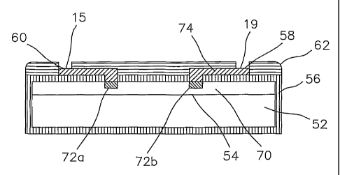
Turning next to FIGS. 6A and 6B, an alternative technique is
shown for providing external hermetic electrical connections through the
encapsulation layer 56 to the electrically conductive pads, e.g., 72a and
72b, on the integrated circuit 70 (shown in the example of FIG. 6B as
CA 02450239 2003-12-10
WO 02/102267 PCT/US02/15810
-16-
extending to the edge of the substrate 52). In this technique, a metallic
(e.g., aluminum, platinum) trace, e.g., trace 74, is formed essentially
parallel to the surface of the substrate 52 and the integrated circuit 70. A
first end of the trace 74 is electrically coupled to the electrically
conductive pad, e.g., pad 72b. A second end 58 of the trace 74 is
exposed through the encapsulation material 56 to form a pad 19
accessible at its outer surface. In the technique shown in FIG. 6B,
hermeticity is achieved via the serpentine routing of the electrical
connection from the second end 58 of trace 74 to the conductive pad 72b
and by the relative length of the metal trace 74, e.g., the length of the
metal trace is preferably at least 100 microns. Preferably, the metal trace
is surrounded by thin, e.g., 1 micron, layers of encapsulation material,
typically deposited as one or more fabrication steps.
Additional electrical connections, e.g., for forming sensing
electrodes El and E2 (see FIG. 6A) may also be formed on the same
surface as the power/communication pads 13, 15, 17, 19 and
'hermetically connected to the integrated circuit 70 in a similar manner.
Such sensing electrodes may be used in combination with the integrated
circuit 70 to form a sensor as described in the aforementioned patents.
Advantageously, when desired, the previously described technique allows
all of the connections, circuitry and sensing electrodes to be formed on
the same surface of the substrate 52 and thus facilitates the fabrication of
multiple, e.g., pairs of, sensors as described further below in the
description of FIGS. 9 and 10.
FIG. 7 shows a partial cross section of a next alternative
embodiment of a technique for providing a hermetic electrical connection
to the semiconductor formed on the substrate. This embodiment is
similar to that shown in reference to FIG. 6A except that additional layers
of interconnected metallic electrically conductive traces, 74', 74"
surrounded by additional encapsulation layers 56', 56", 56"' are used to
further enhanced the hermeticity of the electrical connection (at some
cost in increased thickness of the package).
CA 02450239 2006-08-02
-17-
Various techniques may be used to apply a coating of
encapsulation layer 56, e.g., alumina insulation, over the substrate 52. A
preferred technique, for example, is to use an ion beam deposition (IBD)
technique. IBD techniques are known in the art, as taught, e.g. in U.S.
Patent Nos. 4,474,827 or 5,508,368.
Using such IBD techniques, or similar techniques, the desired
alumina or other layer 56 may be deposited on all sides of the substrate
52 as illustrated in FIG. 8. As seen in FIG. 8, the substrate 52 is placed
on a suitable working surface 401 that is rotatable at a controlled speed.
The working surface 401 with the substrate 52 thereon (once the circuitry
and electrodes have been formed thereon) is rotated while a beam 421 of
ions exposes the rotating surface. Assuming the substrate 52 has six
sides, five of the six sides are exposed to the beam 421 as it rotates,
thereby facilitating application of the desired layer of alumina onto the five
exposed sides of the object. After sufficient exposure, the object is
turned over, thereby exposing the previously unexposed side of the
substrate to the beam, and the process is repeated. In this manner, four
of the sides of the substrate 52 may be double exposed but such double
exposure simply results in a thicker encapsulation layer 56 of alumina on
the double-exposed sides.
Other techniques, as are known in the art, may also be used to
apply the alumina encapsulation layer 56 to the object.
The steps typically followed in applying an encapsuiation layer 56
of alumina to the substrate 52 include:
(a) Sputtering a layer of titanium of about 300 A thick over any
metal conductor or other object that is to be coated with the alumina.
(b) If selective application of the alumina to the object is to be
made, spinning a photosensitive polyamide onto the substrate.
(c) Applying a mask that exposes those areas where alumina is not
to be applied.
(d) Shining ultraviolet (UV) light through the mask to polymerize the
polyamide. Where the UV light illuminates the polyamide is where
CA 02450239 2006-08-02
-18-
aluminum oxide will not be deposited. Thus, the polymerizations of the
polyamide is, in effect, a negatively acting resist.
(e) Developing the photoresist by washing off the unpolymerized
polyamide with xylene, or an equivalent substance. Once the
unpolymerized polyamide has been washed off, the ceramic (or other
component) is ready for aluminum oxide deposition.
(f) If selective application of the alumina is not to be made, i.e., if
alumina is to be applied everywhere, or after washing off the
unpolymerized polyamide, depositing aluminum oxide to a prescribed
thickness, e.g., between 4 and 10 microns, e.g., 6 microns, over the
subject using ion enhanced evaporation (or sputtering), IBD, or other
suitable application techniques.
(g) During application of the coating, rotate and/or reposition the
substrate as required in order to coat all sides of the substrate, e.g., as
shown in FIG. 8, with a coating of sufficient thickness. This step may
require several iterations, e.g., incrementally depositing a thin layer of
alumina, checking the layer for the desired thickness or properties, and
repeating the repositioning, depositing, and checking steps as required
until a desired thickness is achieved, or until the coating exhibits desired
insulative and/or hermeticity properties.
(h) Breaking or scribing the aluminum oxide that resides over the
polyamide, if present, with a diamond scribe, or laser, controller by a
computerized milling machine. This permits a pyrana solution, explained
below, to get under the oxide for subsequent lift off of the aluminum
oxide.
(i) Lifting off the polyamide and unwanted aluminum oxide after
soaking the substrate in pyrana solution (H2SO4 x H202 x 2 heated to
60 C). Soaking should occur for 30 to 60 minutes, depending on the
thickness of the polyamide layer.
The above described coating method is substantially the same as
that disclosed in the referenced U.S. Patent No. 6,043,437. It should be
apparent to one of
CA 02450239 2003-12-10
WO 02/102267 PCT/US02/15810
-19-
ordinary skill in the art that the aforementioned IBD techniques may be
adapted to selectively deposit a layer of platinum or the like of a
biocompatible electrically conductive metal to form the via and electrodes
used to provide an external electrical interconnection to the
semiconductor formed within. Advantageously, by using such an IBD
technique, the platinum or the like metallic layer can be made sufficiently
uniform to provide a hermetic connection.
FIG. 9 illustrates a sensor assembly 100 formed by placing two
sensor substrates 50 back-to-back so that the electrodes of both sensor
substrates face outward. The protective encapsulation layer 56 is not
shown in FIG. 9, but it is presumed to be present.
FIG. 10 depicts the use of the sensor assembly 100 of FIG. 9
within a sheath 102 and membrane 104 so as to form an electrochemical
sensor assembly 110. The sheath 102 surrounds the sensor assembly
100 and forms a reservoir therein into which a suitable solution 108, e.g.,
a saline solution, is held. The membrane 104 surrounds the sheath 102.
Pockets 106 are formed in the membrane 104 over a selected working
electrode. A suitable enzyme 107 is placed inside of the pockets.
Windows 109 expose the enzyme 107 to the surrounding environment
held in the pockets 106.
Operation of the electrochemical sensor assembly 110 may be
substantially as described in the '163 patent and the other previously
referenced patents. However, in the aforedescribed structure of sensor
assembly 110, the sensing windows 109 are located on both sides of the
assembly, thereby providing a broader exposure coverage or "view" for
the operation of the sensor.
As described above, it is thus seen that the present invention
provides and implantable sensor having electrodes and electronic
circuitry, where the electronic circuitry and electrodes are formed on or in
the same substrate material, e.g., a semiconductor substrate of the same
type used in the formation of complementary metal oxide semiconductor
(CMOS) integrated circuits.
CA 02450239 2003-12-10
WO 02/102267 PCT/US02/15810
-20-
It is a further seen that the invention provides and implantable
sensor, including electrodes and electronic circuitry, that does not require
a lid or cover for hermetically sealing hybrid electronic circuitry on one
side of a substrate; thereby allowing the sensor to be significantly thinner
than would otherwise be possible.
While the invention herein disclosed has been described by means
of specific embodiments and applications thereof, numerous
modifications and variations could be made thereto by those skilled in the
art without departing from the scope of the invention set forth in the
claims. For example, it is generally desirable that the corners of the
assembly be rounded (see corner 62 in FIG. 6B) to further ensure
hermeticity. Sandblasting and acid etching techniques can accomplish
this rounding. Furthermore, while pads, e.g., 19, are generally positioned
within a shallow cavity in the encapsulation layer 56, it may be desired to
bond conductive beads or pads to assist external connection or to
stagger/layer the surrounding encapsulation layer to minimize any stress
on external connections to the pads, e.g., 19. Such variations are
considered to be within the scope of the present invention. It is therefore
to be understood that within the scope of the claims, the invention may be
practiced otherwise than as specifically described herein.