Note: Descriptions are shown in the official language in which they were submitted.
CA 02451825 2003-12-02
1
POLYCRYSTALLINE DIAMOND WITH IMPROVED ABRASION RESISTANCE
FIELD OF THE.INVENTION
The present invention is related most generally to cutting elements, and a
method for forming the same. More particularly, the invention is directed to a
cutting
element having an ultra hard polycrystalline cutting layer formed using
chromium
carbide.
BACKGROUND OF THE INVENTION
Cutting elements such as shear cutters for rock bits, for example, typically
have
a body (or substrate), which has a contact face. An ultra hard layer is bonded
to the.
contact face of the body by a sintering process to form a cutting layer
sometimes
referred to as a"cutting table". The body is generally made from tungsten
carbide-cobalt (sometimes referred to simply as "tungsten carbide" or
"carbide"), while
the ultra-hard layer is a polycrystalline ultra hard materiai layer, such as
polycrystal#ine
diamond ("PCD") or polycrystalline cubic boron nitride ("PCBN"). There is
typically a
matrix of binder material within the poiycrystalline material.
Common problems that -plague cutting elements having an ultra-hard material
layer such as PCD or PCBN bonded to the carbide substrate, are chipping,
spalling,
partial fracturing, cracking or exfoliation of the cutting table. These
problems result in
the eariy failure of the ultra-hard layer and thus, in a shorter operating
life for the cutting
element. Typically, these problems may be the result of peak (high magnitude)
.25 stresses generated on the ultra-hard layer at the region in which the
layer makes
contact with an extemal surface, such as when the cutting layer makes contact
with
earthen formations during driiling. For example, generally, cutting elements
are
mounted onto a drag bit body at a negative rake angle. Consequently, the
region of the
cutting element that makes contact with an earthen formation includes a
portion of the
ultra-hard material layer upper surface circumferential edge. This portion of
the layer
is subjected to the highest impact loads.
The ultra hard material layer is generally formed of a plurality of particles
compacted and sintered together. It is desirable to improve the abrasion
resistance of
the ultra hard material layer. Increasing the abrasion resistance of PCD
materials for
example, is desirable as it aNows the user to cut, drill or machine a greater
amount-of
-1-
CA 02451825 2006-08-03
the workpiece without wear of the cutting element. Historically, an increase
in
abrasion resistance has been achieved by reducing the grain size of the PCD.
Toughness is sacrificed, however, as finer-grained PCD materials are less
robust and more prone to chipping than coarser grades. Accordingly, much of
the research into shear cutter type cutting elements has focused on making a
more durable, abrasion-resistant ultra hard material layer, as well as making
a
better interface between the ultra hard material layer and the substrate.
It is also important that the substrate of the cutting element be durable.
One common substrate material is cemented tungsten carbide. Cemented
tungsten carbide generally refers to tungsten carbide ("WC") particles
dispersed
in a binder metal matrix, such as iron, nickel, or cobalt, often referred to a
s
"WC/Co" system. Tungsten carbide in a cobalt matrix is the most common form
of cemented tungsten carbide, which is further classified by grades based on
the
grain size of WC and the cobalt content.
Another common problem that plagues cutting elements having an ultra
hard material layer bonded to a carbide substrate is the formation of
extremely
large, undesirable carbide grains along the interface formed between the
carbide
substrate and the ultra hard material layer. This is particularly true of
tungsten
carbide grains when the favored substrate of WC/Co is used. If not controlled,
tungsten carbide grains having grain sizes in the tens and hundreds of
microns,
may form at the interface between the tungsten carbide substrate and the ultra
hard material layer. The presence of such WC particles may cause stress
fractures and the early delamination of the ultra hard material layer from the
substrate. It is therefore desirable to suppress the formation and incidence
of
WC grains at the interface.
Accordingly, there exists a need for improving various characteristics of
the ultra hard material layer, such as abrasion resistance, without
compromising
other characteristics of the ultra hard material layer. Correspondingly, there
exists a need for a manufacturing process for forming cutting elements and the
like, which includes such improved characteristics.
-2-
CA 02451825 2006-08-03
SUMMARY OF THE INVENTION
The present invention is directed to a cutting element.
Accordingly, the present invention provides a cutting element comprising
a substrate having an end surface, and an ultra hard layer over said end
surface,
said ultra hard layer comprising a polycrystalline material, chromium and
carbon,
wherein said polycrystalline material comprises polycrystalline diamond, and
wherein said substrate is formed of WC/Co and said ultra hard layer is
directly
bound to said end surface and forms an interface therewith, said interface
characterized by an absence of WC grains having a grain size greater than an
average grain size of said substrate.
In one embodiment, the substrate may be formed of a composition of
tungsten carbide and a substrate binder material, and the ultra hard cutting
layer
formed of polycrystalline diamond or polycrystalline cubic boron nitride. The
ultra hard layer may further include a matrix of binder material therein.
The present invention also provides a drill bit comprising a cutting element,
said
cutting element comprising a substrate having and end surface, and an ultra
hard layer joined to said end surface, said ultra hard layer comprising a
polycrystalline material, chromium and carbon, wherein said substrate is
formed
of WC/Co and said ultra hard layer is formed of polycrystalline diamond and is
directly bonded to said end surface thereby forming an interface therewith,
said
interface characterized by an absence of WC grains having a grain size greater
than an average grain size of said substrate.
The present invention also provides a cutting element comprising a
substrate having an end surface, and an ultra hard layer over said end
surface,
said ultra hard layer comprising a polycrystalline material, chromium and
carbon,
wherein said ultra hard material layer has a granite log abrasion test wear
ratio
of at least 2 x 10⁶.
The present invention also provides a cutting element comprising a
substrate having an end surface, and an ultra hard layer over said end
surface,
said ultra hard layer comprising a polycrystalline material, chromium and
carbon,
wherein said substrate is formed of WC/Co and said ultra hard layer is
directly
-3-
CA 02451825 2007-05-02
,a t
bound to said end surface and forms an interface therewith, said interface
characterized by an absence of WC grains having a grain size greater than an
average grain size of said substrate.
The present invention also provides a cutting element comprising a
substrate having an end surface, and an ultra hard material layer over said
end surface, said ultra hard material layer comprising a polycrystalline
material, chromium and carbon, wherein a transition layer is interposed
between said substrate and said ultra hard material layer.
According to various exemplary embodiments, a transition layer may
be used in the cutting element, between the substrate and ultra hard cutting
layer. The present invention also provides a bit incorporating the various
exemplary cutting elements.
BRIEF DESCRIPTION OF THE DRAWINGS
The invention is best understood from the following detailed description
when read in conjunction with the accompanying drawings. It is emphasized
that, according to common practice, the various features of the drawings are
not to-scale. On the contrary, the dimensions of the various features are
arbitrarily expanded or reduced for clarity. Like numerals denote like
features
throughout the specification and drawings. Included are the following figures:
FIG. 1 is a flow chart of a method of manufacturing a cutting element
according to an exemplary embodiment of the present invention;
-3a-
CA 02451825 2003-12-02
1
FIG. 2 is a perspective view of a cutting element according to an exemplary
embodiment of the present invention;
FIG. 3 is a perspective view of a cutting element according to another
exemplary
embodiment of the present invention;
FIG. 4 is a graphical representation of normalized granite log abrasion test
wear
ratio score comparing conventional polycrystalline diamond to polycrystalline
diamond
formed according to the present invention;
FIG. 5 is a graphical. representation showing the effects of chromium carbide
addition upon granite log abrasion scores for PCD;
FIG. 6 is a graphical representation of granite log abrasion test scores of.
PCD
having various percentages of chromium carbide;
FIG. 7 is a graphical representation of drop tower impact test scores and
shows
the effect of adding chromium carbide to PCD; and
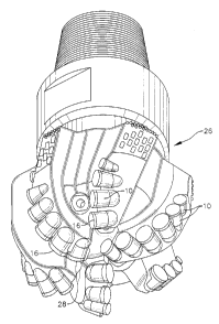
FIG. 8 is a perspective view of a bit body outfitted with exemplary embodiment
cutting.elements of the present invention.
DETAILED DESCRIPTION OF THE INVENTION
The present invention provides an ultra hard polycrystalline layer that
exhibits
improved abrasion resistance without sacrificing toughness. In one
illustrative
embodiment, the present invention finds application in cutting elements and
earth
boring bits incorporating cutting elements used for removing earth. The
present
invention also finds application in other cutting elements and other tooling
elements in
which an ultra hard layer is advantageously utilized. More particularly, the
present
invention is directed to an ultra hard cutting layer metallurgically bonded to
a substrate,
the ultra hard cutting layer formed of a polycrystalline material and
including chromium
carbide and/or chromium and carbon. The polycrystalline material may be PCD or
PCBN, for example. The present invention is also directed to a bit body
incorporating
the cutting elements. The present invention is further directed to a method
for
manufacturing a cutting element including the ultra hard cutting layer.
FIG. 1 shows a flow chart that illustrates a manufacturing sequence of the
present invention used to form an exemplary cutting element of the present
invention.
At step 101, substrate material is provided. According to one exemplary
embodiment,
step 101 includes providing a pre-formed solid substrate. According to.this
embodiment,
-4-
CA 02451825 2003-12-02
1
at step 103, a layer of ultra hard particles and chromium carbide; is provided
over a
surface of the solid substrate. The ultra hard particles and chromium carbide
may be
provided in powder form or in a pre-formed sheet that incorporates a binder.
In powder
form, the layer may also include a binder material. High pressure, high
temperature
("HPHT") processing is then used to convert the layer of ultra hard particles,
chromium
carbide and binder material, to a. layer of ultra hard polycrystalline
material, and to
metallurgically join the ultra hard polycrystalline layer to the solid
substrate during the
same operation, at step 105. The binder material preferably forms what is
often
described as a binder matrix within the ultra hard polycrystalline materiai,
and the ultra
hard polycrystalline layer also includes chromium and carbon from the chromium
carbide. In this embodiment, the solid substrate may take on various shapes
and may
be formed of various materials.
According to another exemplary embodiment of the invention, the substrate
material may be provided in powder form at step 101 along with a binder
material. The
high pressure, high temperature processing step 105, causes the substrate
material to
solidify, the ultra hard particles etc., to be converted to a layer of ultra
hard
polycrystalline material as above, and the ultra hard polycrystalline layer to
be bonded
to the solid substrate.
According to either of the aforementioned exemplary embodiments, one or more
optional intermediate layers may be formed by providing intermediate layer
material at
optional step 102, between the substrate material and the layer of ultra hard
material.
The intem-iediate, or transition, layer(s) between the substrate and the
polycrystalline
ultra hard cutting layer have properties intermediate to the substrate and the
polycrystalline layer. According to this embodiment, one or more transition
layers are
formed interposed between the substrate and the ultra hard layer.
For illustrative purposes, the present invention is described with respect to
a
shear cutter type of cylindrtical cutting element having an ultra hard
polycrystalline
cutting layer formed over an end surface of the cylinder, as shown in FIG: 2.
It should
be understood that the cutting element configuration illustrated in FIG. 2 is
intended to
be exemplary only and that the cutting element may take on various other
shapes and
also that the ultra hard polycrystalline cutting layer may be formed on
various surfaces
of the variously shaped substrates, in other exemplary embodiments.
-5-
CA 02451825 2003-12-02
1
FIG. 2 shows an exemplary cutting element 10 having a generally cylindrical
shape. The body of the cutting element is formed of a substrate material 12
which is
a generally cylindrical member in the illustrated embodiment. In an exemplary
embodiment, substrate 12 may be formed of cemented tungsten carbide. Cemented
tungsten carbide generally refers to tungsten carbide particles dispersed in a
substrate
binder metal matrix such as iron, nickel, or cobalt, forming what is often
referred to as
a"WC/CoH system. The WC/Co system may be further classified by grades based on
the grain size of the WC and the cobalt content. Various grades may be used.
Other
substrate materials may be used in other exemplary embodiments. Wear resistant
materials suitable for use as the substrate may be selected from compounds of
carbide
and metals selected from-Groups IVB, VB, VIB, and VIIB of the Periodic Table
of the
Elements. Examples of other such carbides include tantalum carbide and
titanium
carbide. Substrate binder matrix materials suitable for use in embodiments of
the
invention include the transition metals of Groups VI, VII, and Vlll of the
Periodic Table
of the Elements. For example, iron and nickel are good substrate binder matrix
materials.
Substrate 12 inciudes end surface 14 which is relatively planar in the
exemplary
embodiment, but may take on other shapes and morphologies in. other
embodiments.
End surface 14 forms an interface with ultra hard layer 16 which is a
polycrystalline
material. Ultra hard layer 16 is also referred to as a cutting table and
includes top
surface 18. Ultra hard layer 16 includes thickness 20 and is metallurgically
bonded to
surface 14 of substrate 12 to produce an interface therebetween. According to
another .
exemplary embodiment such as illustrated in FIG. 3, one or more transition
layers such
as optional transition layer 22 may be present at the interface between the
ultra hard
layer 16 and substrate 12. Returning to FIG. 2, a conterminous boundary is
formed
between ultra hard layer 16 and substrate 12 in the absence of the optional
transition
layer(s). In an exemplary embodiment, thickness 20 may be on the order of one
or a
few millimeters but other thicknesses may be used in other exemplary
embodiments.
An aspect of the present invention is the method for forming the described
cutting element. According to the exemplary embodiment in which a.solid
substrate is
provided, and also according to the exemplary embodiment in which a powdered
substrate material is provided, the substrate or substrate material is placed
in a can in
a high pressure apparatus along with a layer of ultra hard particles.that witl
form the
-6-
CA 02451825 2003-12-02
1
ultra hard.cutting layer such as ultra hard layer 16 shown in FIGS. 2 and S.
The can is
typically formed of niobium, but other materials may be used in other
exempiary
embodiments. In addition to the aforementioned substrate embodiments, a
combination sofid/powder substrate may be utilized where appropriate.
Chromium carbide and a binder are mixed in the layer of ultra hard particies.
The uitrahard layer with chromium carbide, and binder may be provided in
powderform
or as a pre-formed sheet that incorporates the binder. The sheet may be p.re-
formed
1 p using a press or by commingling under high shear compaction. Suitable
binder
materials include the transition metals of Groups Vi, VII and Vlii of the
Periodic Table
of Elements, such as cobalt (Co), iron (Fe), manganese (Mn) and nickel (Ni),
although
other suitable binder materiais may be used alternatively.
The particles of ultra hard materiai used to form ultra hard layer 16 may be
diamond powder, cubic boron nitride powder or other suitable powders of ultra
hard
materiais that may be converted to a polycrystaiiine materiai. In addition to
the ultra
hard material powder and the binder material, the chromium carbide is included
in this
layer at a weight percentage which may range from 0.25 to 15 percent by weight
of the
layer. In other embodiments, as much as 50 percent by weight of chromium
carbide
may be used. In an exemplary embodiment, chromium carbide in the form of Cr3C2
may be used but other stoichiometries or combinations thereof may be used as
the
chroniium carbide component.
The components are placed in the can to provide the desired shape to the ultra
hard layer 16 and to shape the substrate when the substrate is provided in
powder
form. The layer or pre-formed sheet of ultra hard particles, chromium carbide
and a
binder, is placed over the substrate surface, end surface 14, and in one
exemplary
embodiment, the layer of material is placed directiy, adjacent the substrate
surface. In
exemplary embodiments such as illustrated in FIGS. 2 and 3, ultra hard layer
16 is a
generally flat layer.
According to the exemplary embodiment in which at least one optional
transition
layer is used, the transition layer materials are provided between the
substrate and the
ultra hard layer. Components are chosen to produce a transition layer or
layers that
have properties, such as elastic properties, intermediate between those of the
substrate
and the polycrystalline layer, for example. The transition layer(s) may
alleviate the
effects of the CTE (coefficient of thermal expansion) mismatch between the
substrate
-7-
CA 02451825 2003-12-02
1
and the polycrystalline layer, for example, and also prevent regions of
abnormal grain
growth at the polycrystalline layer interface. In the embodiment in which the
substrate
is a WC/Co system and the ultra hard polycrystalline layer a PCD material, for
example,
the transition layer(s) prevent regions of abnormal grain growth and
delamination due
to. the presence of large tungsten carbide grains at the interface between the
polycrystalline ultra hard layer and the substrate. The
intermediate/transition layer(s)
also suppress the migration of binder species from the substrate into the
polycrystalline
1 p layer. Such a phenomena is often referred to as infiltration.
The ultra hard layer and substrate components are brought to a sufficiently
high
temperature and pressure in a sintering process that converts the layer of
ultra hard
particles with chromium carbide and a binder, to an ultra hard polycrystalline
layer, and,
in the embodiment in which the substrate is provided as a powder or as a
combination
solid/powder, to solidify the substrate. The optional transition layer or
layers are also
solidified if present. The high pressure high temperature "HPHT" sintering
process
converts this layer of ultra hard particles and chromium carbide to an ultra
hard
polycrystalline layer that includes a matrix of the binder material and has
incorporated
chromium and carbon from the chromium carbide. In other words, the binder
material
fills the void spaces at the trfpie points within the polycrystalline
material.
The chromium and carbon are present in the binder matrix phase of the ultra
hard polycrystalline layer. Applicants believe the chromium and carbon to be
present
as one or more phases of chromium carbide. In an exemplary embodiment with
cobalt
as the binder material and PCD as the polycrystalline material, x-ray mapping
imaging
established that chromium is uniformly dispersed throughout the cobalt matrix
phase
in the PCD. According to each of the above embodiments, the ultra hard layer
is
formed directly and metallurgically bonded to the substrate surface, such as
in the
illustrated embodiment of FIG. 2 in which ultra hard layer 16 forms a
conterminous
boundary with end surface 14 of substrate 12 in the absence of any optional
transition
layers. If an optional transition layer or layers are present, the ultra hard
layer 16 is
bonded to one of the transition layers. Optional transition layer22 is
illustrated in FIG. 3
which also shows ultra hard layer. 16 bonded to exemplary transition layer 22.
In an exemplary embodiment, cobalt is added as the binder material, to the
powder layer used to form ultra hard layer 16, and ultra hard layer 16 is
formed to
include a cobalt matrix therewithin. Such an addition of cobalt prior to the
HPHT
-8-
CA 02451825 2003-12-02
1
process used to form ultra hard layer 16, may obviate the need to rely upon
cobalt
infiltration from the substrate to provide a suitable (cobalt) matrix within
ultra hard layer
16.
Applicants have discovered that polycrystalline ultra hard layer 16 formed
using
chromumcarbide additive, ischaracterized byan increased abrasion resistance
without
compromising its toughness or hardness. The hardness of atypical
polycrystalline ultra
hard layer, characterized by a conventional Vickers hardness measurement, may
be
in the vicinity of 4,000 kg/mm2 or greater. The average grain size of the
polycrystaiiine
diamond or polycrystalline cubic boron nitride may lie within the range of 2-
75 microns,
but may vary in other exemplary embodiments. The increased abrasion resistance
may
be described as an increased resistance to attrition of materials of the ultra
hard layer
due to abrading action between the grains of the ultra hard layer and the test
or working
surface.
Aconventional test for quantifying abrasion resistance is the granite log
abrasion
test ("GLT") which involves machining the surface of a rotating cylinder of
granite. Barre
.granite, for example, is a commonly used granite for this type of test. In an
exemplary
test, the log is rotated at an average of 630 surface feet per minute (192
mpm) past a
half inch (13mm) diameter cutting disk. There is an average depth of cut of
0.02in
(0.5mm) and an average removal rate of 0.023in3/second (0.377cmg/seoond). The
cutting element being tested, has a back rake of 15 in the granite log
abrasion test.
One determines a wear ratio defined as volume of log removed to volume of
cutting tool
removed. With a standard PCD cutting tool made without chromium carbide, the
wear
ratio is approximately 1 x 10⁶, that is, the ratio of volume of granite log
removed to
volume of cutting tool removed, is approximately 1,000,000:1.
FIG. 4 is a graphical representation illustrating granite log abrasion testing
results
for the granite log abrasion resistance test parameters described above, and
using
Barre granite. In FIG. 4, the.effect of chromium carbide addition to a PCD
layer is
illustrated. !n the left hand side bar graph, the effect of chromium carbide
addition is
shown for a fine grain (15-35 micron) PCD cutting layer and on the right side,
the effect
of chromium carbide addition is shown for a coarse grain, about 45 microns or
greater,
PCD cutting layer. The GLT wear ratio is normalized to account for multiple
granite
logs. It can be seen that the ultra hard polycrystalline layer formed using
chromium
carbide, includes an abrasion resistance which is at least 50% greaterthan the
abrasion
-9-
CA 02451825 2003-12-02
1
resistance of the standard PCD. For the fine grain PCD, it can be seen that
approximately a 75-80% increase in abrasion resistance is achieved due to the
addition
of chromium carbide. The GLT wear ratio of the fine grain PCD sample formed
using
the chromium carbide addftive, is in the vicinity of 2.4 x 1W. FIG. 4
illustrates that the
enhancement and performance is greater in the finer grain size material. Each
of the
chromium carbide cutting layer samples evaluated in FIG. 4 was prepared using
a 0.5
weight percent of chromium carbide in the powder used to form the ultra hard
PCD
cutting layer.
FIG. 5 is a graphical representation showing the effects of CrsC2 addition, on
granite log abrasion scores. The sample evaluated in FIG. 5 was also a PCD
sample
prepared with a 0.5 weight percentage of CrsC2 in the powder used to form the
polycrystalline ultra hard cutting layer. FIG. 5 represents aWeibull plot
conunonly used
for displaying a non-normal distribution of data samples and shows the effect
of CrSC2
addition which produces a significantly increased normalized GLT score for the
Cr.3C2
samples.
FIG. 6 is a graphical representation showirig the effect of varying the
percentage
of chromium carbide additions to a course grained PCD cutting layer as
evidenced by
a granite log abrasion testing. FIG. 6 shows a percentage improvement in the
GTLtest
score and indicates that as the weight percentage of chromium carbide added to
the
PCD increases from 0 to 1% to 5%, the improvement in the GLT test result
improves
by about 17% and about 23%, respectively, compared to PCD which was formed
without the chromium carbide additive.. The weight percentages shown in FIG. 6
again
represent the weight percentage of the chromium carbide in the powder material
used
to form the ultra hard cutting layer.
Another advantage of the addition of chromium carbide to the ultra hard
cutting
layer, according to the present invention, is that the toughness of the
polycrystalline
layer is not compromised. In fact, FIG. 7 shows that toughness is enhanced.
FIG. 7
is a graphical representation showing the effect of 1.37 wt /o chromium
carbide addition
on drop tower impact testing, and includes testing on two PCD samples. Drop
tower
impact testing is one indirect way of evaluating material toughness and is a
conventional test that measures impact energy and is well known in the art.
The results
are normalized for comparative purposes. A higher normalized impact test score
indicates a tougher material. As can be seen from FIG. 7, a toughness
improvement
-10-
CA 02451825 2003-12-02
1
of approximately 13% occurs for the sample with chromium carbide. The bar
graph on
the leftof FIG. 7 shows a standard PCD sample which was formed without the
addition
of chromium carbide. The bar graph on the right represents ultra hard PCD
layers
formed by the addition-of 1.37 wt%chromium carbide to the layer of ultra hard
particles
and represents multiple samples.
Yet another advantage of the present invention is the suppression of
abnormally
large grain growth at the interface between the polycrystalline, ultra hard
cutting layer
and the substrate. For the exemplary embodiment in which the substrate is a
WC/Co
substrate and the ultra hard cutting layer is PCD, applicants have discovered
that the
addition of chromium carbide to the PCD suppresses the formation of WC grains
at the
interface. More particularly, the chromium carbide addition suppresses the
incidence
of large, WC grains which may have grain sizes on the order of tens to
hundreds of
microns, at the interface. Such regions of abnormal tungsten carbide grain
growth are
often called eruptions. These regions of abnormal grain growth extend into the
ultra
hard layer and create inhomogeneous regions in the PCD. Depressions or pits
may
then be visible in the PCD upon removal of the carbide substrate. Moreover,
when
large WC grains are formed at the interface between the substrate and a thin
PCD
layer, for example, a PCD layer having a thickness between 0.16mm and 0.3mm,
metal
spots may. form on the surface of the PCD as the abnormally large WC grains
essentially extend through the PCD layer. The present invention therefore also
alleviates this problem by suppressing the incidence of larger WC grains at
the
interface. The produced interface is characterized as being substantially free
of WC.
grains having a grain size larger than the average grain size of the
substrate. In an
exemplary embodiment, the size, of WC.grains in a substrate may range from 1
to 10
microns, but in other exemplary embodiments, the WC grain sizes may range from
0.1
to 20 microns or larger. The reduction or elimination of WC grains from the
interface
reduces stress and minimizes or eliminates fracturing at the interface which
could cause
the early delamination of the ultra hard layer from the substrate.
Applicants believe that the volume percentage of chromium carbide, or chromium
and carbon, within ultra hard layer 16, may range from 0.25 volume percent to
50
volume percent after sintering. The preferred volume percentage is determined
by the
cutting layer characteristics sought, and the upper limit of the amount of
chromium
-11-
CA 02451825 2003-12-02
1
carbide added is determined by the point at which a loss of continuity of
polycrystalline
grains is produced. Such loss of continuity is undesirable.
In one illustrative embodiment, the cutting elements 10 of the present
invention
are mounted in exemplary drag bit 26 as shown in FIG. 8, and contact the
earthen
formation along edge 28, during drilling. This arrangement is intended to be
exemplary
only and cutting elements 10 may be used in various other arrangements in
other
embodiments.
The preceding merely illustrates the principles of the invention. It will thus
be
appreciated that those skilled in the art wil!. be able to devise various
arrangements
which, although not explicitly described or shown herein, embody the
principles of the
invention and are included within its scope and spirit. Furtherniore, all
examples and
conditional language recited herein are pryncipally intended expressly to be
only for
pedagogical purposes and to aid in understanding the principles of the
invention and
the concepts contributed by the inventors to furthering the art, and are to be
construed
as being without limitation to such specifically recited examples and
conditions.
Moreover, all statements herein reciting principles, aspects, and
embodiments.of the
invention, as well as specific examples thereof, are intended to encompass
both
structural and the functional equivalents thereof. Additionally, it is
intended that such
equivalents include both currently known equivalents and equivalents developed
in the
future, i.e., any elements developed that perfomn the same function,
regardless -of
structure. The scope of the present invention, therefore, is not intended to
be fimited to
the exemplary embodiments shown and described herein.. Rather, the scope and
spirit
of the present invention is embodied by the appended claims. ..
35
-12-