Note: Descriptions are shown in the official language in which they were submitted.
CA 02452637 2007-06-27
- 1 -
VISIBLE-LIGHT-RESPONSIVE PHOTOACTIVE COATING,
COATED ARTICLE, AND METHOD OF MAKING SAME
[0001]
1. Field of the Invention
[0002] The present invention relates to methods of depositing
photoactive coatings on a substrate (e.g., a glass sheet or a
continuous float glass ribbon), to methods of making
photocatalytic and/or hydrophilic coatings that exhibit
photoactivity upon irradiation with visible light, and to
articles of manufacture prepared according to the methods.
2. Technical Considerations
[0003] For many substrates, e.g., glass substrates such as
architectural windows, automotive transparencies, and aircraft
windows, it is desirable for good visibility that the surface
of the substrate is substantially free of surface
contaminants, such as common organic and inorganic surface
contaminants, for as long a duration as possible.
Traditionally, this has meant that these surfaces are cleaned
frequently. This cleaning operation is typically performed by
manually wiping the surface with or without the aid of
CA 02452637 2003-12-31
WO 03/006393 PCT/US02/22234
- 2 -
chemical cleaning solutions. This approach can be labor,
time, and/or cost intensive. Therefore, a need exists for
substrates, particularly glass substrates, having surfaces
that are easier to clean than existing glass substrates and
which reduce the need or frequency for such manual cleaning.
[0004] It is known that some semiconductor metal oxides can
provide a photoactive (hereinafter "PA") coating. The terms
"photoactive" or "photoactively" refer to the photogeneration
of a hole-electron pair when illuminated by radiation of a
particular frequency, usually ultraviolet ("UV") light. Above
a certain minimum thickness, these PA coatings are typically
photocatalytic (hereinafter "PC"). By "photocatalytic" is
meant a coating having self-cleaning properties, i.e., a
coating which upon exposure to certain electromagnetic
radiation, such as UV, interacts with organic contaminants on
the coating surface to degrade or decompose the organic
contaminants. In addition to their self-cleaning properties,
these PC coatings are also typically hydrophilic, i.e. water
wetting with a contact angle with water of generally less than
20 degrees. The hydrophilicity of the PC coatings helps
reduce fogging, i.e. the accumulation of water droplets on the
coating, which fogging can decrease visible light transmission
and visibility through the coated substrate.
[0005] A problem with these conventional PC coatings is
that they typically exhibit photoactivity or photocatalysis
only upon exposure to ultraviolet (UV) light in wavelengths
shorter than about 380 nanometers (nm). This means that the
PC coatings make use of only about 3% to 5% of the solar
energy that reaches the earth, which can necessitate the use
of a UV light source (such as a conventional mercury or black
lamp) in order to provide sufficient energy for
photocatalysis.
[0006] In order to address this problem, attempts have been
made to modify conventional PC coatings to shift the
photoabsorption band of the coating material from the UV
region into the visible region (400 nm to 800 nm) of the
electromagnetic spectrum. For example, U.S. Patent No.
CA 02452637 2003-12-31
WO 03/006393 PCT/US02/22234
- 3 -
6,077,492 to Anpo et al. discloses a method of shifting the
photoabsorption band of titanium oxide photocatalysts from the
UV region into the visible light region by high-energy ion
implantation of selected metal ions into the photocatalyst.
Subsequent investigation of this ion implantation method has
determined that the photoabsorption band shift into the
visible region requires not only high-energy ion implantation
but also calcination in oxygen of the metal ion-implanted
titanium oxide (Use Of Visible Light. Second-Generation
Titanium Oxide Photocatalysts Prepared By The Application Of
An Advanced Metal Ion-Implantation Method, M. Anpo, Pure Appl.
Chem., Vol. 72, No. 9, pp. 1787-1792 (2000)). EP 1,066,878
discloses a sol-gel method of doping titania with minute
amounts of selected metal ions to shift the photoabsorption
band of the titania into the visible region.
[0007] However, these ion implantation and sol-gel coating
methods are not economically or practically compatible with
certain application conditions or substrates. For example, in
a conventional float glass process, the float glass ribbon in
the molten metal bath can be too hot to accept the sol due to
evaporation or chemical reaction of the solvent used in the
sol. Conversely, when the sol is applied to substrates that
are below a specific temperature for the formation of
crystalline forms of the catalyst, the sol-coated substrates
are reheated. Reheating to a temperature sufficient to
calcinate the coating or form the crystallized photocatalyst
can require a substantial investment in equipment, energy, and
handling costs, and can significantly decrease production
efficiency. Further, reheating a sodium containing substrate,
such as soda-lime-silica glass, to a teinperature sufficient to
calcinate the coating increases the opportunity for sodium
ions in the substrate to migrate into the coating. This
migration can result in what is conventionally referred to as
"sodium ion poisoning" of the deposited coating. The presence
of these sodium ions can reduce or destroy the photocatalytic
activity of the PC coating. Moreover, the ion-implantation
and sol-gel methods typically result in thick coatings, e.g.,
CA 02452637 2003-12-31
WO 03/006393 PCT/US02/22234
- 4 -
several microns thick, which may have an adverse effect on the
optical and/or aesthetic properties of coated articles.
Typically, as the thickness of the PC coating increases, the
light transmittance and the reflectance of the coating go
through a series of minimums and maximums due to optical
interference effects. The reflected and transmitted color of
the coating also varies due to these optical effects. Thus,
coatings thick enough to provide the desired self-cleaning
properties can have undesirable optical characteristics.
[0008] Therefore, it would be advantageous to provide a
method of making a PA coating with photoabsorption in the
visible region that is compatible with a conventional float
glass process and/or an article made in accordance with the
method which reduce or eliminate at least some of the above-
described drawbacks.
SU1rIlrlARY OF THE INVENTION
[0009] A method is provided for forming a coating by
depositing a precursor composition over at least a portion of
a substrate surface by a CVD coating device. The precursor
composition includes a photoactive coating precursor material,
such as a metal oxide or semiconductor metal oxide precursor
material, and a photoabsorption band modifying precursor
material. In one embodiment, the coating is deposited over a
float glass ribbon in a molten metal bath. In another
embodiment, the coating is deposited over a float glass ribbon
after exiting the molten metal bath but prior to entering a
heat treatment device, such as an annealing lehr. The
resultant coating is one that results in at least
hydrophilicity, e.g., photoactive hydrophilicity, of a coating
on a substrate and can also result in photocatalytic activity
sufficient to be a photocatalytic coating.
[0010] Another method of forming a photoactive coating
having a photoabsorption band in the visible region of the
electromagnetic spectrum includes depositing a precursor
composition over at least a portion of a float glass ribbon in
a molten metal bath by a CVD coating device. The precursor
composition includes at least one titania precursor material.
CA 02452637 2007-06-27
- 5 -
In one embodiment, the titania precursor material includes
titanium and oxygen, e.g., an alkoxide, such as but not limited
to titanium methoxides, ethoxides, propoxides, butoxides, and the
like or isomers thereof, such as but not limited to titanium
isopropoxide, tetraethoxide, and the like. In another
embodiment, the titania precursor material comprises titanium
tetrachloride. The precursor composition also includes at least
one other precursor material having a metal selected from
chromium (Cr), vanadium (V), manganese (Mn), copper (Cu), iron
(Fe), magnesium (Mg), scandium (Sc), yttrium (Y), niobium (Nb),
molybdenum (Mo), ruthenium (Ru), tungsten (W), silver (Ag), lead
(Pb), nickel (Ni), rhenium (Re), or any mixtures or combinations
containing one or more thereof. In one embodiment, the other
precursor material can be an oxide, alkoxide, or mixtures
thereof.
(0011] An additional method of the invention includes
depositing a sodium ion diffusion barrier layer over at least a
portion of a substrate, depositing a photoactive coating over the
barrier layer, and implanting one or more selected metal ions
into the photoactive coating by ion-implantation to form a
photoactive coating having an absorption band including at
least one wavelength in the range of 400nm to 800nm.
[0012] An article of the invention includes a substrate
having at least one surface and a coating deposited over at
least a portion of the substrate surface. The coating includes
a photoactive coating material, such as titania, and at
least one additional material selected from chromium (Cr),
vanadium (V), manganese (Mn), copper (Cu), iron (Fe),
magnesium (Mg), scandium (Sc), yttrium (Y), niobium (Nb),
molybdenum (Mo), ruthenium (Ru), tungsten (W), silver (Ag),
lead (Pb), nickel (Ni), rhenium (Re), or any mixtures
or combinations containing one or more thereof. In one
CA 02452637 2003-12-31
WO 03/006393 PCT/US02/22234
- 6 -
embodiment, the coating is deposited over the substrate by
chemical vapor deposition.
DESCRIPTION OF THE DRAWINGS
[0013] Fig. 1 is a sectional view (not to scale) of a
portion of a substrate having a photoactive coating of the
invention deposited thereon;
[0014] Fig. 2 is a side view (not to scale) of a coating
process for applying a photoactive metal oxide coating of the
invention onto a glass ribbon in a molten metal bath for a
float glass process; and
[0015] Fig. 3 is a side view (not to scale) of an
insulating glass unit incorporating features of the invention.
DESCRIPTION OF THE INVENTION
[0016] As used herein, spatial or directional terms, such
as "inner", "outer", "above", "below", "top", "bottom", and
the like, relate to the invention as it is shown in the
drawing figures. However, it is to be understood that the
invention can assume various alternative orientations and,
accordingly, such terms are not to be considered as limiting.
Further, all numbers expressing dimensions, physical
characteristics, processing parameters, quantities of
ingredients, reaction conditions, and the like used in the
specification and claims are to be understood as being
modified in all instances by the term "about". Accordingly,
unless indicated to the contrary, the numerical values set
forth in the following specification and claims are
approximations that can vary depending upon the desired
properties sought to be obtained by the present invention. At
the very least, and not as an attempt to limit the application
of the doctrine of equivalents to the scope of the claims,
each numerical value should at least be construed in light of
the number of reported significant digits and by applying
ordinary rounding techniques. Moreover, all ranges disclosed
herein are to be understood to encompass any and all subranges
subsumed therein. For example, a stated range of "1 to 10"
CA 02452637 2007-06-27
- 7 -
should be considered to include any and all subranges between
(and inclusive of) the minimum value of 1 and the maximum value
of 10; that is, all subranges beginning with a minimum value of 1
or more and ending with a maximum value of 10 or less, e.g., 5.5
to 10. Further, as used herein, the terms "deposited over" or
"provided over" mean deposited or provided on but not necessarily
in surface contact with. For example, a coating "deposited over"
a substrate does not preclude the presence of one or more other
coating films of the same or different composition located
between the deposited coating and the substrate. Additionally,
all percentages disclosed herein are "by weight" unless indicated
to the contrary. All root mean square roughness values are those
determinable by atomic force microscopy by measurement of the
root mean square (RMS) roughness over a surface area of one
square micrometer.
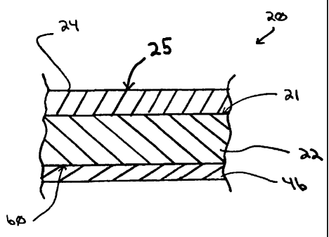
(0017] Referring now to Fig. 1, there is shown an article 20
having features of the present invention. The article 20
includes a substrate 22 having a first surface 21 and a second
surface 60. The substrate 22 is not limiting to the invention
and can be of any desired material having any desired
characteristics, such as opaque or transparent substrates. By
"transparent" is meant having a visible light transmittance of
greater than 0% to 100%. By "opaque" is meant having a visible
light transmittance of 0%. By "visible light" is meant
electromagnetic energy having a wavelength in the range of 400
nanometers (nm) to 800 nm. Examples of suitable substrates
include, but are not limited to, plastic substrates (such as
polyacrylates, polycarbonates, and polyethyleneterephthalate
(PET)); metal substrates; enameled or ceramic substrates; glass
substrates; or mixtures or combinations thereof. For example,
the substrate can be conventional untinted soda-lime-silica-
glass, i.e. "clear glass", or can be tinted or otherwise colored
glass, borosilicate glass, leaded glass, tempered, untempered,
CA 02452637 2003-12-31
WO 03/006393 PCT/US02/22234
- 8 -
annealed, or heat strengthened glass. The glass can be of any,
type, such as conventional float glass, flat glass, or a float
glass ribbon, and can be of any composition having any optical
properties, e.g., any value of visible transmission,
ultraviolet transmission, infrared transmission, and/or total
solar energy transmission. Types of glass suitable for the
practice of the invention are described, for example but not
to be considered as limiting, in United States Patent Nos.
4,746,347; 4,792,536; 5,240,886; 5,385,872; and 5,393,593.
For example, the substrate 22 can be a float glass ribbon, a
glass pane of an architectural window, a skylight, one pane of
an insulating glass unit, a mirror, a shower door, glass
furniture (e.g., glass tabletops, glass cabinets, etc.) or a
ply for a conventional automotive windshield, side or back
window, sun roof, or an aircraft transparency, just to name a
few.
[0018] A photoactively-modified (hereinafter "PM") coating
24 of the invention can be deposited over at least a portion
of the substrate 22, e.g., over all or a portion of a major
surface of the substrate 22, such as over all or a portion of
the surface 21 or the surface 60. In the illustrated
embodiment, the PM coating 24 is shown on the surface 21. As
used herein, the term "photoactively modified" refers to a
material or coating which is photoactive and which includes at
least one additive or dopant that acts to shift and/or widen
the photoabsorption band of the material compared to that of
the material without the additive. By "photoabsorption band"
is meant the range of electromagnetic radiation absorbed by a
material to render the material photoactive. The PM coating
24 can be photocatalytic, photoactively hydrophilic, or both.
By "photoactively hydrophilic" is-meant a coating in which the
contact angle of a water droplet on the coating decreases with
time as a result of exposure of the coating to electromagnetic
radiation in the photoabsorption band of the material. For
example, the contact angle can decrease to a value less than
15 , such as less than 10 , and can become superhydrophilic,
e.g., decrease to less than 5 , after sixty minutes of
CA 02452637 2003-12-31
WO 03/006393 PCT/US02/22234
- 9 -
exposure to radiation in the photoabsorption band of the
material having an intensity of 24 W/m2 at the PM coating
surface. Although photoactive, the coating 24 may not
necessarily be photocatalytic to the extent that it is self-
cleaning, i.e., may not be sufficiently photocatalytic to
decompose organic material like grime on the coating surface
in a reasonable or economically useful period of time.
[0019] The PM coating 24 of the invention includes (1) a
photoactive coating material and (2) an additive or dopant
configured to widen or shift the photoabsorption band of the
coating compared to that of the coating without the dopant
material. The photoactive coating material (1) includes at
least one metal oxide, such as but not limited to, one or more
metal oxides or semiconductor metal oxides, such as titanium
oxides, silicon oxides, aluminum oxides, iron oxides, silver
oxides, cobalt oxides, chromium oxides, copper oxides,
tungsten oxides, zinc oxides, zinc/tin oxides, strontium
titanate, and mixtures thereof. The metal oxide can include
oxides, super-oxides or sub-oxides of the metal. The metal
oxide can be crystalline or at least partially crystalline.
In one exemplary coating of the invention, the photoactive
coating material is titanium dioxide. Titanium dioxide exists
in an amorphous form and three crystalline forms, i.e., the
anatase, rutile and brookite crystalline forms. The anatase
phase titanium dioxide is particularly useful because it
exhibits strong photoactivity while also possessing excellent
resistance to chemical attack and excellent physical
durability. However, the rutile phase or combinations of the
anatase and/or rutile phases with the brookite and/or
amorphous phases are also acceptable for the present
invention.
[0020] The photoabsorption band widening or shifting
material (2) can be any material that widens or shifts the
photoabsorption band of the resultant coating to extend at
least partly into, or extend further into, the visible region
of the spectrum (i.e., widens or shifts the photoabsorption
band to include at least one wavelength in the range of 400 nm
CA 02452637 2003-12-31
WO 03/006393 PCT/US02/22234
- 10 -
to 800 mm not in the photoabsorption band of the coating
without the dopant material (2)). In one exemplary
embodiment, the material (2) includes at least one of chromium
(Cr), vanadium (V), manganese (Mn), copper (Cu), iron (Fe),
magnesium (Mg), scandium (Sc), yttrium (Y), niobium (Nb),
molybdenum (Mo), ruthenium (Ru), tungsten (W), silver (Ag),
lead (Pb), nickel (Ni), rhenium (Re), or any mixtures or
combinations containing any one or more thereof. The material
(2) is present in the PM coating 24 in an amount sufficient to
widen or shift the photoabsorption band of the coating 24 to
extend at least partly into, or extend further into, the
visible region without adversely impacting the desired coating
performance, e.g., reflectivity, transmittance, color, etc.
Additionally, in the practice of the invention, the material
(2) does not necessarily have to be concentrated at or near
the coating surface 21 but, rather, can be deposited in such a
manner that it is dispersed or incorporated into the bulk of
the coating 24.
[0021] The PM coating 24 should be sufficiently thick so as
to provide an acceptable level of photoactivity, e.g.,
photocatalytic activity and/or photoactive hydrophilicity, for
a desired purpose. There is no absolute value which renders
the PM coating 24 "acceptable" or "unacceptable" because
whether a PM coating 24 has an acceptable level of
photoactivity varies depending largely on the purpose and
conditions under which the PM coated article is being used and
the performance standards selected to match that purpose.
However, the thickness of the PM coating 24 to achieve
photoactive hydrophilicity can be much less than is needed to
achieve a commercially acceptable level of photocatalytic
self-cleaning activity. For example, in one embodiment the PM
coating 24 can have a thickness in the range of 10 A to 5000
A, where thicker coatings in this range can have
photocatalytic self-cleaning activity for at least some period
of time as well as hydrophilicity. As the coatings get
thinner in this range, photocatalytic self-cleaning activity
typically decreases in relation to performance and/or
CA 02452637 2007-06-27
- 11 -
duration. As coating thickness decreases in such ranges as 50 A
to 3000 A, e.g., 100 A to 1000 A, e.g., 200 A to 600 A, e.g., 200
A to 300 A, photocatalytic self-cleaning activity may be
immeasurable but photoactive hydrophilicity can still be present
in the presence of selected electromagnetic radiation, e.g.,
within the photoabsorption band of the material.
[0022] In another aspect of the invention, the outer surface
25 of the PM coating 24 of the invention can be much smoother
than previous self-cleaning coatings while still maintaining its
photoactive hydrophilicity and/or photocatalytic activity. For
example, the PM coating 24, in particular the top or outer
surface 25 of the coating, can have an RMS surface roughness of
less than 5 nm even for thin coatings in the above ranges, such
as 200 A to 300 A, e.g., less than 4.9 nm, e.g., less than 4 nm,
e.g., less than 3 nm, e.g., less than 2 nrn, e.g., less than 1 nm
e.g., 0.3 nm to 0.7 nm.
[0023] In a still further aspect of the invention, the PM
coating 24 can be made denser than previous hydrophilic, self-
cleaning coatings. For example, the PM coating 24 can be
substantially non-porous. By "substantially non-porous" is meant
that the coating is sufficiently dense that the coating can
withstand a conventional hydrofluoric acid test in which a drop
of 0.5 weight percent (wt. %) aqueous hydrofluoric acid (HF)
solution is placed on the coating and covered with a watch glass
for 8 minutes (mins) at room temperature. The HF is then rinsed
off and the coating visually examined for damage. An alternative
HF immersion test is described in Industrial Engineering
Chemistry & Research, Vol. 40, No. 1, page 26, 2001 by Charles
Greenberg. The denser PM coating 24 of the invention provides
more protection to the underlying substrate against chemical
attack than previous more porous self-cleaning coatings and also
is harder and more scratch resistant than previous sol-gel
applied self-cleaning coatings.
CA 02452637 2003-12-31
WO 03/006393 PCT/US02/22234
- 12 -
[0024] The PM coating 24 can be deposited directly on,
i.e., in surface contact with, the surface 21 of the substrate
22 as shown in Fig. 1. Even with a sodium-containing
substrate, such as soda-lime-silica glass, thin PM coatings 24
of the invention, e.g., less than 1000A, should not be
rendered non-photoactive by sodium in the substrate when the
coating is applied by the in-bath method described below.
Therefore, an easier to clean soda-lime-silica glass can be
made without a sodium barrier layer between the glass and the
PM coating 24 of the invention. Optionally, such a barrier
layer could be used.
[0025] Alternatively, one or more other layers or coatings
can be interposed between the PM coating 24 and the substrate
22. For example, the PM coating 24 can be an outer or the
outermost layer of a multilayer stack of coatings present on
substrate 22 or the PM coating 24 can be embedded as one of
the layers other than the outermost layer within such a multi-
layer stack. By "an outer layer" is meant a layer receiving
sufficient exciting electromagnetic radiation, e.g., radiation
within the photoabsorption band of the layer material, to
provide the coating with sufficient photoactivity to be at
least photoactively hydrophilic if not necessarily
photocatalytic. In one embodiment, the PM coating 24 is the
outermost coating on the substrate 22.
[0026] A PM coating 24 of the invention can be formed on
the substrate 22 by any conventional method, such as ion-
implantation, spray pyrolysis, chemical vapor deposition
(CVD), or magnetron sputtered vacuum deposition (MSVD). In
the ion-implantation method, metal ions are implanted into the
coating by high voltage acceleration. In the spray pyrolysis
method, an organic or metal-containing precursor composition
having (1) a metal oxide precursor material, e.g., a titania
precursor material, and (2) at least one photoabsorption band
modifying precursor material, i.e., a dopant material (such as
an organometallic precursor material), is carried in an
aqueous suspension, e.g. an aqueous solution, and is directed
toward the surface of the substrate 22 while the substrate 22
CA 02452637 2007-06-27
- 13 -
is at a temperature high enough to cause the precursor
composition to decompose and to form a PM coating 24 on the
substrate 22. In a CVD method, the precursor composition is
carried in a carrier gas, e.g., nitrogen gas, and directed toward
the substrate 22. In the MSVD method, one or more metal-
containing cathode targets are sputtered under reduced pressure
in an inert or oxygen-containing atmosphere to deposit a sputter
coating over substrate 22. The substrate 22 can be heated during
or after coating to cause crystallization of the sputter coating
to form the PM coating 24. For example, one cathode can be
sputtered to provide the metal oxide precursor material (1) and
another cathode can be sputtered to provide the dopant material
(2). Alternatively, a single cathode already doped with the
desired dopant material can be sputtered to form the PM coating
24.
[0027] Each of the methods has advantages and limitations
depending upon the desired characteristics of the PM coating 24
and the type of glass fabrication process. For example, in a
conventional float glass process molten glass is poured onto a
pool of molten metal, e.g., tin, in a molten metal (tin) bath to
form a continuous float glass ribbon. Temperatures of the float
glass ribbon in the tin bath generally range from 1203 C (2200 F)
at the delivery end of the bath to 592 C (1100 F) at the exit end
of the bath. The float glass ribbon is removed from the tin bath
and annealed, i.e. controllably cooled, in a lehr before being
cut into glass sheets of desired length and width. The
temperature of the float glass ribbon between the tin bath and
the annealing lehr is generally in the range of 480 C (896 F) to
580 C (1076 F) and the temperature of the float glass ribbon in
the annealing lehr generally ranges from 204 C (400 F) to 557 C
(1035 F) peak. U.S. Patent Nos. 4,466,562 and 4,671,155 provide
a discussion of the float glass process.
[0028] The CVD and spray pyrolysis methods may be preferred
over the MSVD method in a float glass process because they are
more compatible with coating continuous substrates, such as
float glass ribbons, at elevated temperatures. Exemplary CVD
CA 02452637 2007-06-27
- 14 -
and spray pyrolysis coating methods are described in U.S. Patent
Nos. 4,344,986; 4,393,095; 4,400,412; 4,719,126; 4,853,257; and
4,971,843.
[0029] In the practice of the invention, one or more CVD
coating apparatus can be employed at several points in the float
glass ribbon manufacturing process. For example, CVD coating
apparatus may be employed as the float glass ribbon travels
through the tin bath, after it exits the tin bath, before it
enters the annealing lehr, as it travels through the annealing
lehr, or after it exits the annealing lehr. Because the CVD
method can coat a moving float glass ribbon yet withstand the
harsh environments associated with manufacturing the float glass
ribbon, the CVD method is particularly well suited to provide the
PM coating 24 on the float glass ribbon in the molten tin bath.
U.S. Patent Nos. 4,853,257; 4,971,843; 5,536,718; 5,464,657;
5,714,199; and 5,599,387, describe CVD coating apparatus and
methods that can be used in the practice of the invention to coat
a float glass ribbon in a molten tin bath.
[0030] For example, as shown in Fig. 2, one or more CVD
coaters 50 can be located in the tin bath 52 above the molten
tin pool 54. As the float glass ribbon 56 moves through the
tin bath 52, the vaporized precursor composition (i.e., the
photoactive coating precursor material (1), e.g., metal oxide
precursor material, and the photoabsorption band modifying
material (2), e.g., an organometallic precursor material), can
be added to a carrier gas and directed onto the top surface 21
of the ribbon 56. The precursor composition decomposes to form
a PM coating 24 of the invention. The material (2) can be at
least partially soluble in the coating precursor material (1),
such as fully soluble in the coating precursor material (1)
under the desired deposition conditions. Any desired amount
of the material (2) to achieve a desired shift of the
photoabsorption band into the visible region can be added
to, mixed into, or solubilized in the coating precursor
CA 02452637 2003-12-31
WO 03/006393 PCT/US02/22234
- 15 -
material (1). Alternatively, the two separate precursors can
be separately vaporized and combined.
[0031] Exemplary coating precursor materials (1) (e.g.,
titania precursor materials) that can be used in the practice
of the present invention to form titanium dioxide PM coatings
24 by the CVD method include, but are not limited to, oxides,
sub-oxides, or super-oxides of titanium. In one embodiment,
the precursor material (1) can include one or more titanium
alkoxides, such as but not limited to titanium methoxide,
ethoxide, propoxide, butoxide, and the like; or isomers
thereof, e.g., titanium isopropoxide, tetraethoxide, and the
like. Exemplary precursor material suitable for the practice
of the invention include, but are not limited to, titanium
tetraisopropoxide (Ti(0C3H7)9) (hereinafter "TTIP") and titanium
tetraethoxide (Ti(0C2H5)4) (hereinafter "TTEt") . Alternatively,
the titania precursor material (1) can be titanium
tetrachloride.
[0032] The photoabsorption band shifting material (2) can
be any material that shifts or widens the photoabsorption band
of the resultant coating to extend at least partly into, or
extend further into, the visible region (400 nm to 800 nm) of
the electromagnetic spectrum. The material can include one or
more of chromium (Cr), vanadium (V), manganese (Mn), copper
(Cu), iron (Fe), magnesium (Mg), scandium (Sc), yttrium (Y),
niobium (Nb), molybdenum (Mo), ruthenium (Ru), tungsten (W),
silver (Ag), lead (Pb), nickel (Ni), rhenium (Re), and/or any
mixtures or combinations thereof. For example, the precursor
material (2) can be a metal oxide or alkoxide. In one
embodiment, the material (2) is at least partially soluble,
e.g., mostly soluble, in the precursor material (1).
Exemplary carrier gases that can be used in the CVD method of
the invention include but are not limited to air, nitrogen,
oxygen, ammonia and mixtures thereof. The concentration of
the precursor composition in the carrier gas can vary
depending upon the specific precursor composition used.
However, it is anticipated that for coatings having a
thickness of about 200 A, the concentration of precursor
CA 02452637 2008-05-08
-- 16 -
composition in the carrier gas will typically be in the range of
0.01 volume % to 0.1 volume %, e.g., 0.01 volume % to 0.06 volume
%, e.g., 0.015 volume % to 0.06 volume %; e.g., 0.019 volume % to
0.054 volume %. For thicker coatings, the precursor compositions
can be higher.
[0033] For the CVD method (as well as the spray pyrolysis
method discussed below), the temperature of the substrate 22 (such
as a float glass ribbon 56) during formation of the PM coating 24
thereon should be within the range which will cause the metal
containing precursor composition to decompose and form a coating
having a desired amount of photoactivity, e.g., photocatalytic
activity, photoactive hydrophilicity, or both. The lower limit of
this temperature range is largely affected by the decomposition
temperature of the selected precursor composition. For the above
listed titanium-containing precursors, the lower temperature limit
of the substrate 22 to provide sufficient decomposition of the
precursor composition is generally in the range of 400 C (752 F) to
500 C (932(F). The upper limit of this temperature range can be
affected by the method of coating the substrate. For example,
where the substrate 22 is a float glass ribbon 56 and the PM
coating 24 is applied to the float glass ribbon 56 in the molten
tin bath 50 during manufacture of the float glass ribbon 56, the
float glass ribbon 56 can reach temperatures in excess of 1000 C
(1832 F). The float glass ribbon 56 can be attenuated or sized
(e.g. stretched or compressed) at temperatures above 800 C
(1472 F). If the PM coating 24 is applied to the float glass
ribbon 56 before or during attenuation, the PM coating 24 can
crack or crinkle as the float glass ribbon 56 is stretched or
compressed respectively. Therefore, the PM coating 24 can be
appl.ied when the float glass ribbon 56 is dimensionally stable
(except for thermal contraction with cooling), e.g., below 800 C
(1472 F) for soda lime silica glass, and the float glass ribbon 56
is at a temperature to decompose the metal-containing precursor,
e.g., above 400 C (752 F).
[0034] For spray pyrolysis, U.S. Patent Nos. 4,719,126;
4,719,127; 4,111,150; and 3,660,061, describe spray pyrolysis
CA 02452637 2008-05-08
- 17 -
apparatus and methods that cari be used with a conventional float
glass ribbon manufacturing process. While the spray pyrolysis
method like the CVD method is well suited for coating a moving
float glass ribbon, the spray pyrolysis has more complex
equipment than the CVD equipment and is usually employed between
the exit end of the tin bath and the entrance end of the
annealing lehr.
[0035] Exemplary metal-containing precursor compositions that
can be used in the practice of the invention to form PM coatings
by the spray pyrolysis method include relatively water insoluble
organometallic reactants, specifically metal acetylacetonate
compounds, which are jet milled or wet ground to a particle size
of less than 10 microns and suspended in an aqueous medium by the
use of a chemical wetting agent. A suitable metal
acetylacetonate precursor material to form a titanium dioxide
containing PM coating is titanyl acetylacetonate (Ti0(C5H70z)2)
A photoabsorption band modifying material, such as described
above, can be mixed with or solubilized into the acetylacetonate
precursor material. In one embodiment, the relative
concentration of the metal acetylacetonate and band shifting
precursor materials in the aqueous suspension ranges from 5 to 40
weight percent of the aqueous suspension. The wetting agent can
be any relatively low foaming surfactant, including anionic,
nonionic or cationic compositions. In one embodiment, the
surfactant is nonionic. The wetting agent is typically added at
0.24% by weight, but can range from 0.01% to 1% or more. The
aqueous medium can be distilled or deionized water. Aqueous
suspensions for pyrolytic deposition of metal-containing films
are described in U.S. Patent No. 4,719,127 particularly at column
2, line 16, to column 4, line 48.
[0036] As will be appreciated by those skilled in the art,
the bottom surface 60 of the float glass ribbon resting directly
on the molten tin (commonly referred to as the "tin side") has
diffused tin in the surface which provides the tin side with a
pattern of tin absorption that is different from the opposing
surface 21 not in contact with the molten tin (commonly referred
to as "the air side"). The PM coating of the invention can be
CA 02452637 2008-05-08
- 18 -
formed on the air side of the float glass ribbon while it is
supported on the tin by the CVD method as described above, on the
air side of the float glass ribbon after it leaves the tin bath
by either the CVD or spray pyrolysis methods, and/or on the tin
side of the float glass ribbon after it exits the tin bath by the
CVD method.
[0037] As an alternative to including oxygen in the
atmosphere of the tin bath to form oxide coatings, the precursor
composition can itself include one or more sources of organic
oxygen. The organic oxygen can be, for example, an ester or
carboxylate ester, such as an alkyl ester having an alkyl group
with a R-hydrogen. Suitable esters can be alkyl esters having a
C2 to CLQ alkyl group. Exemplary esters which can be used in the
practice of the invention are described in WO 00/75087.
[0038] With respect to MSVD, U.S. Patent Nos. 4,379,040;
4,861,669; 4,900,633; 4,920,006; 4,938,857; 5,328,768; and
5,492,750, describe MSVD apparatus and methods to sputter coat
metal oxide films on a substrate, including a glass substrate.
The MSVD process is not generally compatible with providing a
PM coating over a float glass ribbon during its manufacture
because, among other things, the MSVD process requires reduced
pressure during the sputtering operation which is difficult
to form over a continuous moving float glass ribbon. However,
the MSVD method is acceptable to deposit the PM coating 24 on
substrate 22, e.g., a glass sheet. The substrate 22 can be
heated to temperatures in the range of 400 C (752 F) to 500 C
(932 F) so that the MSVD sputtered coating on the substrate
crystallizes during deposition process thereby eliminating a
subsequent heating operation. Heating the substrate during
sputtering is not a preferred method because the additional
heating operation during sputtering can decrease throughput.
Alternatively, the sputter coating can be crystallized within
the MSVD coating apparatus directly and without post heat
CA 02452637 2003-12-31
WO 03/006393 PCT/US02/22234
- 19 -
treatment by using a high-energy plasma, but again because of
its tendency to reduce throughput through an MSVD coater, this
is not a preferred method.
[0039] An exemplary method to provide a PM coating
(especially a PM coating of 300 A or less and having an RMS
surface roughness of 2 nm or less) using the MSVD method is to
sputter a dopant containing coating on the substrate, remove
the coated substrate from the MSVD coater, and thereafter heat
treat the coated substrate to crystallize the sputter coating.
For example, but not limiting to the invention, a target of
titanium metal doped with at least one photoabsorption band
shifting material selected from chromium (Cr), vanadium (V),
manganese (Mn), copper (Cu), iron (Fe), magnesium (Mg),
scandium (Sc), yttrium (Y), niobium (Nb), molybdenum (Mo),
ruthenium (Ru), tungsten (W), silver (Ag), lead (Pb), nickel
(Ni), rhenium (Re), and/or mixtures or combinations thereof
can be sputtered in an argon/oxygen atmosphere having 5-500
oxygen, such as 20% oxygen, at a pressure of 5-10 millitorr to
sputter deposit a doped titanium dioxide coating of desired
thickness on the substrate 22. The coating as deposited is
not crystallized. The coated substrate is removed from the
coater and heated to a temperature in the range of 400 C
(752 F) to 600 C (1112 F) for a time period sufficient to
promote formation of the crystalline form of titanium dioxide
to render photoactivity. In one embodiment, the substrate is
heated for at least an hour at temperature in the range of
400 C (752 F) to 600 C (1112 F). Where the substrate 22 is a
glass sheet cut from a float glass ribbon, the PM coating 24
can be sputter deposited on the air side and/or the tin side.
[0040] The substrate 22 having the PM coating 24 deposited
by the CVD, spray pyrolysis or MSVD methods can be
subsequently subjected to one or more post-coating annealing
operations. As may be appreciated, the time and temperatures
of the anneal can be affected by several factors, including
the makeup of substrate 22, the makeup of PM coating 24, the
thickness of the PM coating 24, and whether the PM coating 24
CA 02452637 2007-06-27
- 20 -
is directly in contact with the substrate 22 or is one layer of a
multilayer stack on substrate 22.
[0041] Whether the PM coating 24 is provided by the CVD
process, the spray pyrolysis process, or the MSVD process, where
the substrate 22 includes sodium ions that can migrate from the
substrate 22 into the PM coating 24 deposited on the substrate
22, the sodium ions can inhibit or destroy the photoactivity,
e.g., photocatalytic activity and/or photoactive hydrophilicity,
of the PM coating 24 by forming inactive compounds while
consuming titanium, e.g., by forming sodium titanates or by
causing recombination of photoexcited charges. Therefore, a
sodium ion diffusion barrier (SIDB) layer can be deposited over
the substrate before deposition of the PM coating 24. A suitable
SIDB layer is discussed in detail in U.S. Patent No. 6,027,766.
With post-coating heating, a sodium barrier layer for sodium
containing substrates, such as soda-lime-silica glass, can be
utilized. For applying the PM coating 24 of the invention in a
molten metal bath, the sodium barrier layer is optional.
[0042] The SIDB layer can be formed of amorphous or
crystalline metal oxides including but not limited to cobalt
oxides, chromium oxides and iron oxides, tin oxides, silicon
oxides, titanium oxides, zirconium oxides, fluorine-doped tin
oxides, aluminum oxides, magnesium oxides, zinc oxides, and
mixtures thereof. Mixtures include but are not limited to
magnesium/aluminum oxides and zinc/tin oxides. As can be
appreciated by those skilled in the art, the metal oxide can
include oxides, super-oxides or sub-oxides of the metal.
While the thickness of the SIDB layer necessary to prevent
sodium ion poisoning of the PM coating varies with several
factors including the time period at which a substrate will be
maintained at temperatures above which sodium ion migration
occurs, the rate of sodium ion migration from the substrate, the
rate of sodium ion migration through the SIDB layer, the
thickness of the PM coating and the degree of photocatalytic
activity required for a given application, typically for most
CA 02452637 2003-12-31
WO 03/006393 PCT/US02/22234
- 21 -
applications, the SIDB layer thickness should be in the range
of at least about 100A, such as at least about 250A, e.g., at
least about 500A thick to prevent sodium ion poisoning of the
PM coating layer. The SIDB layer can be deposited over
substrate 22 by any conventional method, such as but not
limited to CVD, spray pyrolysis, or MSVD methods. Where the
spray pyrolysis or CVD methods are employed, the substrate 22
can be maintained at a temperature of at least about 400 C
(752 F) to ensure decomposition of the metal-containing
precursor to form the SIDB layer. The SIDB layer can be
formed by other methods, including the sol-gel method, which
sol-gel method as noted above is typically not compatible with
the manufacture of a glass float ribbon.
[0043] A tin oxide SIDB layer, such as a fluorine doped tin
oxide SIDB, can be deposited on a substrate by spray pyrolysis
by forming an aqueous suspension of dibutyltin difluoride
(C4H9)2SnF2 and water and applying the aqueous suspension to the
substrate via spray pyrolysis. In general, the aqueous
suspension typically contains between 100 to 400 grams of
dibutyltin difluoride per liter of water. Wetting agents can
be used as suspension enhancers. During the preparation of
the aqueous suspension, the dibutyltin difluoride particles
can be milled to an average particle size of 1 to 10 microns.
The aqueous suspension can be vigorously agitated to provide a
uniform distribution of particles in suspension. The aqueous
suspension is delivered by spray pyrolysis to the surface of a
substrate which is at a temperature of at least about 400 C
(752 F), such as about 500 C to 700 C (932 F to 1292 F),
whereupon the aqueous suspension pyrolyzes to form a tin oxide
SIDB layer. As may be appreciated, the thickness of SIDB
layer formed by this process can be controlled by, among other
parameters, the coating line speed, the dibutyltin difluoride
concentration in the aqueous suspension and the rate of
spraying.
[0044] Alternatively the tin oxide SIDB layer can be formed
by the CVD method on the substrate from a metal-containing
precursor such as a monobutyltintrichloride vapor (hereinafter
CA 02452637 2007-06-27
- 22 -
"MBTTCL") in an air carrier gas mixed with water vapor. The
MBTTCL vapor can be present in a concentration of at least about
0.5% in the air carrier gas applied over substrate while the
substrate is at a temperature sufficient to cause the deposition
of a tin containing layer e.g. at least about 4002C (9529F), such
as about 5002C to 8002C (9322F to 14729F), to form the tin oxide
SIDB layer. As may be appreciated the thickness of the SIDB
layer formed by this process can be controlled by, among other
parameters, the coating line speed, the concentration of MBTTCL
vapor in the air carrier gas and the rate of carrier gas flow.
[0045] An SIDB layer formed by the MSVD process is described
in U.S. Patent No. 5,830,252, entitled "Alkali Metal Diffusion
Barrier Layer", which discloses the formation of alkali metal
diffusion barriers. The barrier layer disclosed therein is
generally effective at thicknesses of about 20 A to about 180A,
with effectiveness increasing as the density of the barrier
increases.
[0046] The PM coatings 24 of the present invention can be
photoactive, e.g., photocatalytic and/or photoactively
hydrophilic, upon exposure to radiation in the ultraviolet range,
e.g., 300 nm to 400 nm, and/or visible range (400 nm to 800 nm)
of the electromagnetic spectrum. Sources of ultraviolet
radiation include natural sources, e.g., solar radiation, and
artificial sources such as a black light or an ultraviolet light
source such as a UVA-340 light source commercially available from
the Q-Panel Company of Cleveland, Ohio.
[0047] As shown in Fig. 1, in addition to the PM coating 24
of the invention, one or more functional coatings 46 can be
deposited on or over the substrate 22. For example, a functional
coating 46 can be deposited over the major surface 60 of the
substrate 22 that is opposite the surface 21. As used herein,
the term "functional coating" refers to a coating which modifies
one or more physical properties of the substrate on which it is
deposited, e.g., optical, thermal, chemical or mechanical
properties, and is not intended to be removed from the substrate
during subsequent processing. The functional coating 46 can have
one or more functional coating films of the same or different
CA 02452637 2007-06-27
- 23 -
composition or functionality. As used herein, the terms "layer"
or "film" refer to a coating region of a desired or selected
coating composition. The film can be homogeneous, non-
homogeneous, or have a graded compositional change. A film is
"homogeneous" when the outer surface or portion (i.e., the
surface or portion farthest from the substrate), the inner
surface or portion (i.e., the surface or portion closest to the
substrate) and the portion between the outer and inner surfaces
have substantially the same composition. A film is "graded" when
the film has a substantially increasing fraction of one or more
components and a substantially decreasing fraction of one or more
other components when moving from the inner surface to the outer
surface or vice versa. A film is "non-homogeneous" when the film
is other than homogeneous or graded. A "coating" is composed of
one or more "films".
[0048] The functional coating 46 can be an electrically
conductive coating, such as, for example, an electrically
conductive heated window coating as disclosed in U.S. Patent Nos.
5,653,903 and 5,028,759, or a single-film or multi-film coating
capable of functioning as an antenna. Likewise, the functional
coating 46 can be a solar control coating, for example, a
visible, infrared or ultraviolet energy reflecting or absorbing
coating. Examples of suitable solar control coatings are found,
for example, in U.S. Patent Nos. 4,898,789; 5,821,001; 4,716,086;
4,610,771; 4,902,580; 4,716,086; 4,806,220; 4,898,790; 4,834,857;
4,948,677; 5,059,295; 5,028,759, and 6,495,251. Similarly, the
functional coating 46 can be a low emissivity coating. "Low
emissivity coatings" allow visible wavelength energy, e.g., 400
nm to about 800 nm (e.g., to about 780 nm), to be transmitted
through the coating but reflect longer-wavelength solar infrared
energy and/or thermal infrared energy and are typically intended
to improve the thermal insulating properties of architectural
glazings. By "low emissivity" is meant emissivity less than 0.4,
such as less than 0.3, e.g., less than 0.2. Examples of low
emissivity coatings are found, for example, in U.S. Patent Nos.
4,952,423 and 4,504,109 and British reference GB 2,302,102. The
functional coating 46 can be a single layer or multiple layer
CA 02452637 2007-06-27
- 24 -
coating and can comprise one or more metals, non-metals, semi-
metals, semiconductors, and/or alloys, compounds, composites,
combinations, or blends thereof. For example, the functional
coating 46 can be a single layer metal oxide coating, a multiple
layer metal oxide coating, a non-metal oxide coating, or a
multiple layer coating.
[0049] Examples of suitable functional coatings for use with
the invention are commercially available from PPG Industries,
Inc. of Pittsburgh, Pennsylvania under the SUNGATE and
SOLARBANO families of coatings. Such functional coatings
typically include one or more anti-reflective coating films
comprising dielectric or anti-reflective materials, such as metal
oxides or oxides of metal alloys, which are preferably
transparent or substantially transparent to visible light. The
functional coating 46 can also include infrared reflective films
comprising a reflective metal, e.g., a noble metal such as gold,
copper or silver, or combinations or alloys thereof, and can
further comprise a primer film or barrier film, such as titanium,
as is known in the art, located over and/or under the metal
reflective layer.
[0050] The functional coating 46 can be deposited in any
conventional manner, such as but not limited to magnetron sputter
vapor deposition (MSVD), chemical vapor deposition (CVD), spray
pyrolysis (i.e., pyrolytic deposition), atmospheric pressure CVD
(APCVD), low-pressure CVD (LPCVD), plasma-enhanced CVD (PEVCD),
plasma assisted CVD (PACVD), thermal or electron-beam
evaporation, cathodic arc deposition, plasma spray deposition,
and wet chemical deposition (e.g., sol-gel, mirror silvering
etc.). For example, U.S. Patent Nos. 4,584,206, 4,900,110, and
5,714,199, disclose methods and apparatus for depositing a metal
containing film on the bottom surface of a glass ribbon by
chemical vapor deposition. Such a known apparatus can be located
downstream of the molten tin bath in the float glass process to
provide a functional coating on the underside of the glass
ribbon, i.e., the side opposite the PM coating of the invention.
Alternatively, one or more other CVD coaters can be located in
the tin bath to deposit a functional coating either above or
CA 02452637 2007-06-27
- 25 -
below the PM coating 24 on the float glass ribbon. When the
functional coating is applied on the PM coating side of the
substrate, the functional coating can be applied in the tin
bath before the PM coating. When the functional coating is on
the opposite side 60 from the PM coating, the functional coating
can be applied after the tin bath in the float process as
discussed above, e.g., on the tin side of the substrate 22 by
CVD or MSVD. In another embodiment, the PM coating 24 can be
deposited over all or a portion of the surface 60 and the
functional coating 46 can be deposited over all or a portion
of the surface 21.
[0051] An exemplary article of manufacture of the invention
is shown in Fig. 3 in the form of an insulating glass (IG)
unit 30. The insulating glass unit has a first pane 32 spaced
from a second pane 34 by a spacer assembly (not shown) and held
in place by a sealant system to form a chamber between the two
panes 32, 34. The first pane 32 has a first surface 36
(number 1 surface) and a second surface 38 (number 2 surface).
The second pane 34 has a first surface 40 (number 3 surface)
and a second surface 42 (number 4 surface). The first surface 36
can be the exterior surface of the IG unit, i.e. the surface
exposed to the environment, and the second surface 42 can be the
interior surface, i.e. the surface forming the inside of the
structure. Examples of IG units are disclosed in U.S. Patent
Nos. 4,193,236; 4,464,874; 5,088,258; and 5,106,663. In one
embodiment shown in Fig. 3, the PM coating 24 can be
positioned on the number 1 or number 4 surfaces, such as on the
number 1 surface. The PM coating 24 reduces fogging and makes
the IG unit 30 easier to clean and maintain. In this
CA 02452637 2003-12-31
WO 03/006393 PCT/US02/22234
- 26 -
embodiment, one or more optional functional coatings 46 as
described above can be deposited over at least a portion of
the number 2, number 3, or number 4 surfaces.
[0052] Advantages of the present invention over the ion-
implantation and sol-gel methods of forming self-cleaning
coatings include an ability to form a thin, dense, PM film on
a substrate as opposed to the generally thicker, porous self-
cleaning coatings obtained with the ion-implantation and sol-
gel coating methods. Still another advantage is that the
method of providing a PM coating according to the present
invention avoids the need to reheat the substrate after
application of the coating or coating precursor as is
practiced in the conventional ion-implantation and sol-gel
methods. Not only does this render the present method less
costly and more efficient, e.g., less equipment costs, less
energy costs, and less production time, but also the
opportunity for sodium ion migration and in turn sodium ion
poisoning of the PM coating 24 of the present invention is
significantly reduced. Further still, the method of the
present invention is easily adapted to the formation of PM
coatings on continuous moving substrates, such as a glass
float ribbon.
[0053] It will be readily appreciated by those skilled in
the art that modifications can be made to the invention
without departing from the concepts disclosed in the foregoing
description. Accordingly, the particular embodiments
described in detail herein are illustrative only and are not
limiting to the scope of the invention, which is to be given
the full breadth of the appended claims and any and all
equivalents thereof.