Note: Descriptions are shown in the official language in which they were submitted.
CA 02464078 2004-04-16
WO 2004/015771 PCT/JP2003/009958
1
D E 5 C R I P T I 0 N
SEMICONDUCTOR DEVICE AND METHOD OF
MANUFACTURING THE SAME
Technical Field
The present invention relates to a semiconductor
device which incorporates a chip-size semiconductor
package, and a method of manufacturing the
semiconductor device.
Background Art
For example, in a semiconductor device called BGA
(Ball Grid Array), a semiconductor chip formed with'
an LSI and the like is mounted on the upper center
surface of a relay board (interposes) slightly larger
in size than the semiconductor chip. Connection
terminals of solder balls are arrayed in a matrix on
the lower surface of the relay board. The relay board
is used to sufficiently increase the size and pitch by
a distribution wire in order to ensure connection
strength and reliability in bonding an external
connection electrode formed on the semiconductor chip
to another circuit board.
FIG. 84 is a sectional view showing an example of
a conventional semiconductor device. A semiconductor
chip 1 has a structure in which a plurality of bump
electrodes 3 of copper or the like are arranged at
the periphery on the lower surface of a silicon
CA 02464078 2004-04-16
WO 2004/015771 - PCT/JP2003/009958
2
substrate 2.
A relay board 4 has a base film 5 slightly larger
in size than the silicon substrate 2 of the semicon-
ductor chip 1. Distribution wires 6 which are
respectively connected to the bump electrodes 3 of the
semiconductor chip 1 are formed on the upper surface of
the base film 5.
The distribution wires 6 are comprised of first
connection pads 7 which are arranged in correspondence
with the bump electrodes 3 of the semiconductor chip 1,
second connection pads 8 which are arrayed in a matrix,
and lead lines 9 which connect the first and second
connection pads 7 and 8. Circular holes 10 are formed
in the base film 5 at portions corresponding to the
centers of the second connection pads 8.
The semiconductor chip 1 is mounted on the upper
center surface of the relay board 4 via an anisotropic
conductive adhesive 11. The anisotropic conductive
adhesive 11 is prepared by adding many conductive
particles 13 into a thermosetting resin 12.
When the semiconductor chip 1 is to be mounted on
the relay board 4, the semiconductor chip 1 is aligned
and simply placed on the upper center surface of the
relay board 4 via the sheet-like anisotropic conductive
adhesive 11.
A predetermined pressure is applied for bonding at
a temperature at which the thermosetting resin 12 sets.
CA 02464078 2004-04-16
WO 2004/015771 PCT/JP2003/009958
3
The bump electrodes 3 then push away the thermosetting
resin 12 and are electrically connected to the upper
surfaces of the first connection pads 7 via the
conductive particles 13. In addition, the lower
surface of the semiconductor chip 1 is adhered to
the upper surface of the relay board 4 via the
thermosetting resin 12.
A resin sealing film 14 made of an epoxy resin is
formed on the entire upper surface of the relay board 4
including the semiconductor chip 1. Solder balls 15
are formed in the circular holes 10, and connected to
the lower surfaces of the second connection pads 8.
Since the second connection pads 8 are arrayed in
a matrix, the solder balls 15 are also arrayed in
a matrix.
The solder ball 15 is larger in size than the bump
electrode 3 of the semiconductor chip 1.. In order to
avoid contact between the solder balls 15, their
arrangement interval must be larger than that of the
bump electrodes 3. When the number of bump electrodes
3 of the semiconductor chip 1 increases, the arrange-
ment region of the solder balls 15 must be set larger
than the size of the semiconductor chip 1 in order to
obtain an arrangement interval necessary for the solder
balls 15. For this purpose, the relay board 4 is
designed slightly larger in size than the semiconductor
chip 1. Of the solder balls 15 arrayed in a matrix,
CA 02464078 2004-04-16
WO 2004/015771 PCT/JP2003/009958 -
4
peripheral solder balls 15 are arranged around the
semiconductor chip 1.
The conventional semiconductor device adopts the
relay board 4 having the distribution wire 6. By
bonding after alignment, the lower surface of the bump
electrode 3 of the semiconductor chip 1 is electrically
connected to the upper surface of the first connection
pad 7 of the distribution wire 6 on the relay board 4
via the conductive particles 13 of the anisotropic
conductive adhesive 11. If the number of bump
electrodes 3 of the semiconductor chip 1 increases
and the size and arrangement interval of the bump
electrodes 3 decrease, alignment becomes very
difficult. By increasing the size of the semiconductor
~-5 chip l, the size and arrangement interval of the bump
electrodes 3 can be increased. However, the number of
semiconductor chips which can be formed from a wafer
greatly decreases, resulting in an expensive semicon-
ductor chip. The semiconductor chips 1 must be bonded
and mounted on the relay board 4 one by one, which
makes the manufacturing process cumbersome. This also
applies to a mufti-chip module type semiconductor
device having a plurality of semiconductor chips.
Disclosure of Invention
It is an object of the present invention to
provide a semiconductor device capable of increasing
the arrangement interval of external connection
CA 02464078 2004-04-16
WO 2004/015771 - PCT/JP2003/009958
electrodes without bonding, and a method of
manufacturing the semiconductor device.
It is another object of the present invention to
provide a semiconductor device manufacturing method
5 capable of manufacturing a plurality of semiconductor
devices at once.
According to an aspect of the present invention,
there is provided a semiconductor device comprising
a semiconductor construction assembly having a
semiconductor substrate which has one surface, the
other surface facing the one surface, and a plurality
of side surfaces between the one surface and the other
surface, and has an integrated circuit element formed
on the one surface, a plurality of connection pads
which are arranged on the one surface and connected
to the integrated circuit element, a protective layer
which is formed to cover the one surface of the
semiconductor substrate and has openings for exposing
the connection pads, and a plurality of conductors
which are connected to the connection pads, arranged on
the protective layer, and have pads
an upper insulating layer which entirely covers
the one surface of the semiconductor construction
assembly including the conductors except the pads
a sealing member which covers at least one side
surface of the semiconductor construction assembly and
upper conductors which are formed on the upper
CA 02464078 2004-04-16
WO 2004/015771 PCT/JP2003/009958
6
insulating layer, and has one ends electrically
connected to the pads and an external connection pads,
respectively, an external connection pad of at least
one of the upper conductors being disposed in a region
corresponding to the sealing member.
According to another aspect of the present
invention, there is provided a semiconductor device
manufacturing method comprising
arranging on a base plate a plurality of
semiconductor construction assemblies in which
a plurality of conductors having pads are formed on
a semiconductor substrate, so as to space apart the
semiconductor construction assemblies from each other;
forming an insulating layer on an entire upper
surface of the base plate including the plurality of
semiconductor construction assemblies;
forming, on an upper surface of the insulating
layer, upper conductors which have connection pads and
are to be connected to corresponding pads of conductors
of the semiconductor construction assemblies, so as to
arrange at least one of the upper conductors on the
insulating layer formed between the semiconductor
construction assemblies and
cutting the insulating layer between the semicon-
ductor construction assemblies to obtain a plurality
of semiconductor devices each having at least one
semiconductor construction assembly in which the
CA 02464078 2004-04-16
WO 2004/015771 PCT/JP2003/009958
7
connection pad of the upper conductors is formed on the
insulating layer in a region outside the semiconductor
construction assembly.
Brief Description of Drawings
FIG. 1 is an enlarged sectional view showing a
semiconductor device according to the first embodiment
of the present invention;
FIG. 2 is an enlarged sectional view showing
a structure prepared in advance in an example of
a method of manufacturing the semiconductor device
shown in FIG. 1;
FIG. 3 is an enlarged sectional view showing
a manufacturing step subsequent to FIG. 2;
FIG. 4 is an enlarged sectional view showing
a manufacturing.step subsequent to FIG. 3;
FIG. 5 is an enlarged sectional view showing
a manufacturing step subsequent to FIG..4';
FIG. 6 is an enlarged sectional view showing
a manufacturing step subsequent to FIG. 5;
FIG. 7 is an enlarged sectional view showing
a manufacturing step subsequent to FIG. 6;
FIG. 8 is an enlarged sectional view showing
a manufacturing step subsequent to FIG. 7;
FIG. 9 is an enlarged sectional view showing
a manufacturing step subsequent to FIG. 8;
FIG. 10 is an enlarged sectional view showing
a manufacturing step subsequent to FIG. 9;
CA 02464078 2004-04-16
WO 2004/015771 - PCT/JP2003/009958
8
FIG. 11 is an enlarged sectional view showing
a manufacturing step subsequent to FIG. 10;
FIG. 12 is an enlarged sectional view showing
a manufacturing step subsequent to FIG. 11;
FIG. 13 is an enlarged sectional view showing
a manufacturing step subsequent to FIG. 12;
FIG. 14 is an enlarged sectional view showing
a manufacturing step subsequent to FIG. 13;
FIG. 15 is an enlarged sectional view showing
a manufacturing step subsequent to FIG. 14;
FIG. 16 is an enlarged sectional view showing
a manufacturing step subsequent to FIG. 15;
FIG. 17 is an enlarged sectional view showing
a manufacturing step subsequent to FIG. 16;
FIG. 18 is an enlarged sectional view showing
a manufacturing step subsequent to FIG. 17;
FIG. 19 is an enlarged sectional view showing
a base member prepared in advance in another example of
the method of manufacturing the semiconductor device
shown in FIG. 1;
FIG. 20 is an enlarged sectional view for
explaining details of a manufacturing step in this
method;
FIG. 21 is an enlarged sectional view showing
a predetermined manufacturing step in still another
example of the method of manufacturing the
semiconductor device shown in FIG. 1;
CA 02464078 2004-04-16
WO 2004/015771 PCT/JP2003/009958
9
FIG. 22 is an enlarged sectional view showing
a manufacturing step subsequent to FIG. 21;
FIG. 23 is an enlarged sectional view showing
the first modification to the semiconductor device
according to the first embodiment of the present
invention;
FIG. 24 is an enlarged sectional view showing
the second modification to the semiconductor device
according to the first embodiment of the present
invention;
FIG. 25 is an enlarged sectional view showing
the third modification to the semiconductor device
according to the first embodiment of the present
invention;
FIG. 26 is an enlarged sectional view showing
the fourth modification to the semiconductor device
according to the first embodiment of the present
invention;
FIG. 27 is an enlarged sectional view showing
the fifth modification to the semiconductor device
according to the first embodiment of the present
invention;
FIG. 28 is an enlarged sectional view showing
the sixth modification to the semiconductor device
according to the first embodiment of the present
invention;
FIG. 29 is an enlarged sectional view showing
CA 02464078 2004-04-16
WO 2004/015771 - PCT/JP2003/009958
the seventh modification to the semiconductor device
according to the first embodiment of the present
invention;
FIG. 30 is an enlarged sectional view showing
5 the eighth modification to the semiconductor device
according to the first embodiment of the present
invention;
FIG. 31 is an enlarged sectional view showing
the ninth modification to the semiconductor device
10 according to the first embodiment of the present
invention;
FIG. 32 is an enlarged sectional view showing the
10th modification to the semiconductor device according
to the first embodiment of the present invention;
FIG. 33 is an enlarged sectional view showing the
11th modification to the semiconductor device according
to the first embodiment of the present invention;
FIG. 34 is an enlarged sectional view showing the
12th modification to the semiconductor device according
to the first embodiment of the present invention;
FIG. 35 is an enlarged sectional view showing the
13th modification to the semiconductor device according
to the first embodiment of the present invention;
FIG. 36 is an enlarged sectional view showing the
14th modification to the semiconductor device according
to the first embodiment of the present invention;
FIG. 37 is an enlarged sectional view showing the
CA 02464078 2004-04-16
WO 2004/015771 - PCT/JP2003/009958
11
15th modification to the semiconductor device according
to the first embodiment of the present invention;
FIG. 38 is an enlarged sectional view for
explaining an initial manufacturing step for the
semiconductor device shown in FIG. 37;
FIG. 39 is an enlarged sectional view showing
a manufacturing step subsequent to FIG. 38;
FIG. 40 is an enlarged sectional view showing
a manufacturing step subsequent to FIG. 39;
FIG. 41 is an enlarged sectional view showing
a manufacturing step subsequent to FIG. 40;
FIG. 42 is an enlarged sectional view showing
a manufacturing step subsequent to FIG. 41;
FIG. 43 is an enlarged sectional view showing
a manufacturing step subsequent to FIG. 42;
FIG. 44 is an enlarged sectional view showing
a manufacturing step subsequent to FIG. 43;
FIG. 45 is an enlarged sectional view showing the
16th modification to the semiconductor device according
to the first embodiment of the present invention;
FIG. 46 is an enlarged sectional view showing the
17th modification to the semiconductor device according
to the first embodiment of the present invention;
FIG. 47 is an enlarged sectional view showing the
18th modification to the semiconductor device according
to the first embodiment of the present invention;
FIG. 48 is an enlarged sectional view showing the
CA 02464078 2004-04-16
WO 2004/015771 PCT/JP2003/009958
12
19th modification to the semiconductor device according
to the first embodiment of the present invention;
FIG. 49 is an enlarged sectional view showing the
20th modification to the semiconductor device according
to the first embodiment of the present invention;
FIG. 50 is an enlarged sectional view for
explaining repair in the semiconductor device shown in
FIG. 48;
FIG. 51 is an enlarged sectional view showing a
semiconductor device according to the second embodiment
of the present invention;
FIG. 52 is an enlarged sectional view showing
an initial manufacturing step for the semiconductor
device shown in FIG. 51;
1.5 FIG. 53 is an enlarged sectional view showing
a manufacturing step subsequent to FIG. 52;
FIG. 54.is an enlarged sectional view showing
a manufacturing step subsequent to FIG. 53;
FIG. 55 is an enlarged sectional view showing
the first modification to the semiconductor device
according to the second embodiment of the present
invention;
FIG. 56 is an enlarged sectional view showing
the second modification to the semiconductor device
according to the second embodiment of the present
invention;
FIG. 5? is an enlarged sectional view showing
CA 02464078 2004-04-16
WO 2004/015771 PCT/JP2003/009958
13
the third modification to the semiconductor device
according to the second embodiment of the present
invention;
FIG. 58 is an enlarged sectional view showing
the fourth modification to the semiconductor device
according to the second embodiment of the present
invention;
FIG. 59 is an enlarged sectional view showing
the fifth modification to the semiconductor device
according to the second embodiment of the present
invention;
FIG. 60 is an enlarged sectional view showing
the sixth modification to the semiconductor device
according to the second embodiment of the present
invention;
FIG. 61 is an enlarged sectional view showing
the seventh modification to the semiconductor device
according to the second embodiment of the present
invention;
FIG. 62 is an enlarged sectional view showing
the eighth modification to the semiconductor device
according to the second embodiment of the present
invention;
FIG. 6f is an enlarged sectional view showing
the ninth modification to the semiconductor device
according to the second embodiment of the present
invention;
CA 02464078 2004-04-16
WO 2004/015771 PCT/JP2003/009958
14
FIG. 64 is an enlarged sectional view showing the
10th modification to the semiconductor device according
to the second embodiment of the present invention;
FIG. 65 is an enlarged sectional view showing the
11th modification to the semiconductor device according
to the second embodiment of the present invention;
FIG. 66 is an enlarged sectional view showing the
12th modification to the semiconductor device according
to the second embodiment of the present invention;
FIG. 67 is an enlarged sectional view showing the
13th modification to the semiconductor device according
to the second embodiment of the present invention;
FIG. 68 is an enlarged sectional view showing the
14th modification to the semiconductor device according
to the second embodiment of the present invention;
FIG. 69 is an enlarged sectional view showing a
semiconductor device according to the third embodiment
of the present invention;
FIG. 70 is an enlarged sectional view for
explaining a method of manufacturing the semiconductor
device shown in FIG. 69;
FIG. 71 is an enlarged sectional view showing
a manufacturing step subsequent to FIG. 70;
FIG. 72 is an enlarged sectional view showing
a manufacturing step subsequent to FIG. 71;
FIG. 73 is an enlarged sectional view showing
a manufacturing step subsequent to FIG. 72;
CA 02464078 2004-04-16
WO 2004/015771 - PCT/JP2003/009958
FIG. 74 is an enlarged sectional view showing
a manufacturing step subsequent to FIG. 73;
FIG. 75 is an enlarged sectional view showing
a manufacturing step subsequent to FIG. 74;
5 FIG. 76 is an enlarged sectional view showing
a manufacturing step subsequent to FIG. 75;
FIG. 77 is an enlarged sectional view showing
the first modification to the semiconductor device
according to the third embodiment of the present
10 invention;
FIG. 78 is an enlarged sectional view showing
the second modification to the semiconductor device
according to the third embodiment of the present
invention;
15 .FIG. 79 is an enlarged sectional view showing
the third modification to the semiconductor device
according to the third embodiment of the present
invention;
FIG. 80 is an enlarged sectional view showing
the fourth modification to the semiconductor device
according to the third embodiment of the present
invention;
FIG. 81 is an enlarged sectional view showing
the fifth modification to the semiconductor device
according to the third embodiment of the present
invention;
FIG. 82 is an enlarged sectional view showing
CA 02464078 2004-04-16
WO 2004/015771 - PCT/JP2003/009958
16
the sixth modification to the semiconductor device
according to the third embodiment of the present
invention;
FIG. 83 is an enlarged sectional view showing
the seventh modification to the semiconductor device
according to the third embodiment of the present
invention; and
FIG. 84 is an enlarged sectional view showing
an example of a conventional semiconductor device.
Best Mode for Carrying Out the Invention
(First Embodiment)
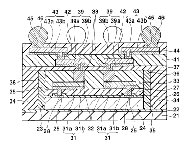
FIG. 1 is a sectional view showing a semiconductor
device according to the first embodiment of the present
invention. The semiconductor device comprises a flat
square base plate 21 made of silicon, glass, ceramic,
a resin, a metal, or the like. An adhesive layer 22 is
formed from an adhesive, pressure sensitive adhesive
sheet, double-sided adhesive tape, or the like on the
upper surface of the base plate 21.
The lower surface of a flat square semiconductor
construction assembly 23 slightly smaller in size
than the base plate 21 is adhered to the upper center
surface of the adhesive layer 22. In this case, the
semiconductor construction assembly 23 is called a CSP
(Chip Size Package), and has a silicon substrate
(semiconductor substrate) 24 which is adhered to
the upper center surface of the adhesive layer 22.
CA 02464078 2004-04-16
WO 2004/015771 - PCT/JP2003/009958
17
Integrated circuit elements which constitute a memory
circuit or control circuit are formed on the
upper center surface of the silicon substrate 24.
A plurality of connection pads 25 which are made of
aluminum or the like and connected to the integrated
circuit elements are arranged around the integrated
circuit. An insulating film 26 made of silicon oxide
or the like is formed on the upper surface of the
silicon substrate 24 except the centers of the
connection pads 25. In practice, many connection
pads 25 are arrayed at the periphery on the upper
surface of the silicon substrate 24. For illustrative
convenience, only a pair of connection pads 25 are
typically shown.
A structure in which the connection pads 25 and
insulating film 26 are formed on the silicon substrate
24 is generally obtained by dicing a semiconductor
substrate in the wafer state into chips. In the first
embodiment, however, no dicing is done in a state in
which the connection pads 25 and insulating film 26 are
formed on a semiconductor substrate in the wafer state.
As will be described later, a semiconductor substrate
in the wafer state is diced after the semiconductor
construction assembly 23 having distribution wires
and columnar electrodes is obtained. The structure of
the semiconductor construction assembly 23 will be
explained.
CA 02464078 2004-04-16
WO 2004/015771 - PCT/JP2003/009958
18
A protective film 27 made of polyimide or the like
is formed on the insulating film 26 formed on the
silicon substrate 24. The centers of the connection
pads 25 are exposed via openings 28 which are formed
in the insulating film 26 and protective film 27.
Distribution wires 31 each comprised of a lower metal
layer 31a and an upper metal layer 31b formed on the
lower metal layer 31a are formed to extend from the
upper surfaces of the connection pads 25 that are
exposed via the openings 28 to predetermined portions
on the upper surface of the protective film 27.
Columnar electrodes 32 are arranged on the upper
surfaces of the connection pads of the distribution
wires 31. Each columnar electrode 32 is formed of
copper and 100 to 200 ,um in height. A sealing film
(insulating film) 33 made of an epoxy resin or the like
is formed on. the upper surface of the. protective film
27 including the distribution wires 31 such that the
upper surface of the sealing film 33 becomes flush with
that of the columnar electrode 32. In this manner,
the semiconductor construction assembly 23 includes
the silicon substrate 24, connection pads 25, and
insulating film 26, and further includes the protective
film 27, distribution wires 31, columnar electrodes 32,
and sealing film 33.
A square frame-like buried member 34 is adhered to
the upper surface of the adhesive layer 22 around the
CA 02464078 2004-04-16
WO 2004/015771 PCT/JP2003/009958
19
semiconductor construction assembly 23. FIG. 1 is a
sectional view in one direction. Even on a section in
a direction perpendicular to FIG. 1, the buried member
34 is adhered to the side surfaces of the semiconductor
construction assembly 23. In other words, the buried
member 34 has a shape surrounding all the side surfaces
of the semiconductor construction assembly 23. In this
case, the buried member 34 can adopt the same material
as that of the base plate 21, or a heat-resistant
circuit board material such as a glass fiber-filled
epoxy resin. The thickness of the buried member 34
is almost equal to the total thickness of the semicon-
ductor construction assembly 23. A relatively narrow
gap 35 is formed between the semiconductor construction
assembly 23 and.the square frame-like buried member .
34 which is arranged outside the semiconductor
construction assembly 23. A sealing film (insulating
film) 36 made of an epoxy resin or the like is filled
in the gap 35 such that the upper surface of the
sealing film 36 becomes almost flush with those of
the sealing film 33 and buried member 34.
A first upper insulating film 37 made of
photosensitive or non-photosensitive polyimide or the
like is formed on the entire upper surfaces of the
semiconductor construction assembly 23, buried member
34, and sealing film 36. Openings 38.are formed at
portions of the first upper insulating film 37 that
CA 02464078 2004-04-16
WO 2004/015771 PCT/JP2003/009958
correspond to the upper center surfaces of the columnar
electrodes 32. First upper distribution wires 39 each
comprised of a first lower metal layer 39a and a first
upper metal layer 39b formed on the first lower metal
5 layer 39a are formed on and from the upper surfaces of
the columnar electrodes 32 that are exposed via the
openings 38 to predetermined portions on the upper
surface of the first upper insulating film 37.
A second upper insulating film 41 made of
10 photosensitive or non-photosensitive polyimide or the
like is formed on the entire upper surface of the first
upper insulating film 37 including the first upper
distribution wires 39. Openings 42 are formed at
portions of the second upper insulating film 41 that
15 correspond to the connection pads of the first upper
distribution wires 39. Second upper distribution wires
43 each comprised of a second lower metal layer.43a.and
a second upper metal layer 43b formed on the second
lower metal layer 43a are formed from the upper
20 surfaces of the connection pads of the first. upper
distribution wires 39 that are exposed via the openings
42 to predetermined portions on the upper surface of
the second upper insulating film 41.
A third upper insulating film 44 made of
photosensitive or non-photosensitive polyimide or the
like is formed on the entire upper surface of the
second upper insulating film 41 including the second
CA 02464078 2004-04-16
WO 2004/015771 - PCT/JP2003/009958
21
upper distribution wires 43. Openings 45 are formed at
portions of the third upper insulating film 44 that
correspond to the connection pads of the second upper
distribution wires 43. Solder balls (projecting
connection terminals) 46 are formed in and on the
openings 45, and connected to the connection pads of
the second upper distribution wires 43. The solder
balls 46 are arrayed in a matrix on the third upper
insulating film 44.
1p As described above, the base plate 21 is slightly
larger in size than the semiconductor construction
assembly 23 in order to set the arrangement region
of the solder balls 46 slightly larger than the size
of the semiconductor construction assembly 23 in
accordance with an increase in the number of connection
pads 25 on the silicon substrate 24 and set the size
and arrangement interval of the connection pads 25
larger than those of the columnar electrodes 32.
The connection pads (portions in the openings 45
of the third upper insulating film 44) of the second
upper distribution wires 43 arrayed in a matrix are
arranged not only in a region corresponding to the
semiconductor construction assembly 23, but also in the
region of the buried member 34 around the semiconductor
construction assembly 23 and the region of the sealing
film 36 filled in the gap 35 between the semiconductor
construction assembly 23 and the buried member 34.
CA 02464078 2004-04-16
WO 2004/015771 PCT/JP2003/009958
22
Of the solder balls 46 arrayed in a matrix, at least
the outermost solder balls 46 are arranged around the
semiconductor construction assembly 23.
In this case, as a modification, all the connec-
tion pads of the second upper distribution wires 43 may
be arranged around the semiconductor construction
assembly 23. The upper ctlstribuLlon wire cam ~~ ~~LmCu
from only one layer, i.e., the first upper distribution
wire 39, and at least the outermost connection pads can
be arranged around the semiconductor construction
assembly 23.
In the semiconductor device, the sealing film
36 and buried member 34 are arranged around the
semiconductor construction assembly 23 in which not
1'5 only the connection pads 25 and insulating film 26, but
also the protective film 27, distribution wires 31,
columnar electrodes 32, sealing film 33, and the like
are formed on the silicon substrate 24. At least the
first upper insulating film 37, and the first upper
distribution wires 39 which are connected to the
columnar electrodes 32 via the openings 38 formed in
the first upper insulating film 37 are formed on the
upper surface of the semiconductor construction
assembly 23.
In this case, the relatively narrow gap 35 is
formed between the semiconductor construction assembly
23 and the square frame-like buried member 34 around
CA 02464078 2004-04-16
WO 2004/015771 - PCT/JP2003/009958
23
the semiconductor construction assembly 23. The
sealing film 36 made of an epoxy resin or the like is
filled in the gap 35. Compared to the absence of any
buried member 34, the amount of sealing film 36 can be
reduced by the volume of the buried member 34. As a
result, the stress by shrinkage in curing the sealing
film 36 made of an epoxy resin or the like can be
reduced, preventing warpage of the base plate 21.
An example of a semiconductor device manufacturing
method will be explained with reference to FIGS. 2
to 18. An example of a method of manufacturing the
semiconductor construction assembly 23 will be
described with reference to FIGS. 2 to 8. As shown in
FIG. 2, a structure in which aluminum connection pads
25, a silicon oxide insulating film 26, and a polyimide
protective film 27 are formed on a silicon substrate
(semiconductor substrate) 24 in the wafer.state, and
the centers of the connection pads 25 are exposed via
openings 28 formed in the insulating film 26 and
protective film;27 is prepared.
As shown in FIG. 3, a lower metal layer 31a is
formed on the entire upper surface of the protective
film 27 including the upper surfaces of the connection
pads 25 that are exposed via the openings 28. In this
case, the lower metal layer 31a is comprised of only
a copper layer formed by electroless plating. However,
the lower metal layer 31a may be comprised of only
CA 02464078 2004-04-16
WO 2004/015771 PCT/JP2003/009958
24
a copper layer formed by sputtering, or a copper layer
formed by sputtering on a thin film layer of titanium
or the like formed by sputtering. This also applies
to the lower metal layers 39a and 43a of upper layers
(to be described later).
A plating resist film 51 is formed and patterned
on the upper surface of the lower metal layer 31a.
Thus, openings 52 are formed in the plating resist film
51 at portions corresponding to formation regions of
distribution wires 31. Copper is electroplated using
the lower metal layer 31a as a plating current path,
thereby forming upper metal layers 31b on the upper
surface of the lower metal layer 31a in the openings 52
of the plating resist film 51. After that, the plating
resist film 51 is peeled.
As shown in FIG. 4, a plating resist film 53 is
formed and. patterned on the upper surface .of th.e lower
metal layer 31a including the upper metal layer 31b.
Thus, openings 54 are formed in the plating resist film
53 at portions corresponding to formation regions of
columnar electrodes 32. Copper is electroplated using
the lower metal layer 31a as a plating current path,
forming the columnar electrodes 32 on the upper
surfaces of the connection pads of the upper metal
layers 31b in the openings 54 of the plating resist
film 53.
The plating resist film 53 is peeled, and
CA 02464078 2004-04-16
WO 2004/015771 PCT/JP2003/009958
unnecessary portions of the lower metal layer 31a are
etched away, using the columnar electrodes 32 and upper
metal layers 31b as a mask. As shown in FIG. 5, the
lower metal layers 31a remain only below the upper
5 metal layers 31b. The remaining lower metal layers 31a
and the upper metal layers 31b formed on the entire
upper surfaces of the lower metal layers 31a form
distribution wires 31.
As shown in FIG. 6, a sealing film 33 made of
10 an epoxy resin is formed on the entire upper surface
of the protective film 27 including the columnar
electrodes 32 and distribution wires 31 such that the
thickness of the sealing film 33 becomes larger than
the height of the columnar electrode 32. In this
15 state, the upper surface of the columnar electrode 32
is covered with the sealing film 33. The upper
surfaces of the sealing film 33 and columnar electrodes
32 are properly polished to expose the upper surfaces
of the columnar electrodes 32, as shown in FIG. 7.
20 Thus, the upper surface of the sealing film 33 and the
exposed upper surfaces of the columnar electrodes 32
are planarized. As shown in FIG. 8, a plurality of
semiconductor construction assemblies 23 shown in
FIG. 1 are obtained after a dicing step of the
25 resultant assembly.
The columnar electrodes 32 formed by
electroplating may be inferably varied in height.
CA 02464078 2004-04-16
WO 2004/015771 PCT/JP2003/009958
26
Thus, the upper surfaces of the columnar electrodes 32
are polished as described above, eliminating variations
in height and making the heights of the columnar
electrodes 32 equal to each other. Polishing of the
upper surfaces of the copper columnar electrodes 32
uses an expensive, high-precision grinder.
An example of manufacturing the semiconductor
device shown in FIG. 1 by using the semiconductor
construction assembly 23 obtained in this manner
will be described. As shown in FIG. 9, a structure in
which an adhesive layer 22 is formed on the entire
upper surface of a base plate 21 capable of forming
a plurality of base plates 21 shown in FIG. 1 is
prepared.
The lower surface of a grid-like buried member 34
is adhered to a predetermined portion on the upper
surface of the adhesive layer 22. For example, the
grid-like buried member 34 is obtained by forming by
die cutting, etching, or the like a plurality of square
openings 34a in a sheet-like buried member 34 made of
silicon, glass, ceramic, a resin, a metal, or the like.
The grid-like buried member 34 may also be formed by
spot facing by adhering the sheet-like buried member 34
to the entire upper surface of the adhesive layer 22.
The lower surface of the silicon substrate 24 of
each semiconductor construction assembly 23 is adhered
to the upper center surface of the adhesive layer 22
CA 02464078 2004-04-16
WO 2004/015771 PCT/JP2003/009958
27
in each opening 34a of the grid-like buried member 34.
In this state, the upper surfaces of the buried member
34 and semiconductor construction assembly 23 are
almost flush with each other. A relatively narrow gap
35 is formed between the semiconductor construction
assembly 23 and the square frame-like buried member 34
around the semiconductor construction assembly 23.
As shown in FIG. 10, a sealing film 36 made of an
epoxy resin or the like is applied by printing or the
like to the entire upper surfaces of the semiconductor
construction assembly 23 and buried member 34 including
the inside of the gap 35. In this state, the upper
surfaces of the semiconductor construction assembly 23
and buried member 34 are covered with the sealing film
36. The uncured sealing film 36 which covers the upper
surfaces of the semiconductor construction assembly 23
and buried member 34 is removed by buff polishing.. .
Consequently, as shown in FIG. 11, the upper surfaces
of the semiconductor construction assembly 23 and
buried member 34 are exposed. In addition, the upper
surface of the portion of the sealing film 36 in
the gap 35 is made almost flush with those of the
semiconductor construction assembly 23 and buried
member 34, substantially planarizing the entire upper
surface. Thereafter, the sealing film 36 is set.
This polishing can use a low-cost, low-precision
buff because the upper surface of the semiconductor
CA 02464078 2004-04-16
WO 2004/015771 PCT/JP2003/009958
28
construction assembly 23, i.e., the upper surface of
the copper columnar electrode 32 is not polished, but
the uncured sealing film 36 covering the upper surfaces
of the semiconductor construction assembly 23 and
buried member 34 is removed. In order to prevent
excessive polishing of the uncured sealing film 36 in
the gap 35 and reduce cure shrinkage of the sealing
film 36, the coated sealing film 36 may be provision-
ally cured by ultraviolet irradiation or heating. If
the flatness is not enough due to large cure shrinkage
of the sealing film 36 in the gap 35, application and
polishing of the sealing resin may be repeated.
As another example of polishing, a low-cost,
low-precision endless polishing belt may be used.
After a part of the endless polishing.belt may be
formed flat, the uncured or provisionally cured sealing
film 36 which covers the upper surfaces of the
semiconductor construction assembly 23 and buried
member 34 may be planarized and polished with the flat
portion of the polishing belt not so as to exceed the .
upper surfaces of the semiconductor construction
assembly 23 and silicon substrate 24 as a polishing
limit surface.
The relatively narrow gap 35 is formed between the
semiconductor construction assembly 23 and the square
frame-like buried member 34 around the semiconductor
construction assembly 23. The epoxy resin sealing film
CA 02464078 2004-04-16
WO 2004/015771 PCT/JP2003/009958
29
36 is filled in the gap 35. Compared to the absence of
any buried member 34, the amount of sealing film 36
can be reduced by the volume of the buried member 34.
As a result, the stress by shrinkage in curing the
epoxy resin sealing film 36 can be reduced, thus
preventing warpage of the base plate 21.
At the end of the polishing step shown in FIG. 11,
a first upper insulating film 37 is formed on the
entire upper surfaces of the semiconductor construction
assembly 23, buried member 34, and sealing film 36
which are almost flush with each other, as shown
in FIG. 12. The first upper insulating film 37 is
made of photosensitive polyimide, photosensitive
polybenzoxazole, a photosensitive epoxy resin,
a photosensitive novolac resin, or a photosensitive
acrylic spiro-ortho-ester resin, and formed into a dry
film. The dry film is laminated by a laminator to form
the first upper insulating film 37. This also applies
to the second and third upper insulating films 41 and
44 (to be described later). The first upper insulating
film 37 may be formed by coating such as printing.
Openings 38 are formed by photolithography at
portions of the first upper insulating film 37 that
correspond to the upper center surfaces of the columnar
electrodes 32. As shown in FIG. 13, a first lower
metal layer 39a is formed on the entire upper surface
of the first upper insulating film 37 including the
CA 02464078 2004-04-16
WO 2004/015771 PCT/JP2003/009958
upper surfaces of the columnar electrodes 32 that are
exposed via the openings 38. A plating resist film 55
is formed and patterned on the upper surface of the
first lower metal layer 39a. Thus, openings 56 are
5 formed in the plating resist film 55 at portions
corresponding to the formation regions of the first
upper distribution wires 39. Copper is electroplated
using the first lower metal layer 39a as a plating
current path, thereby forming first upper metal layers
10 39b on the upper surfaces of the portions of the first
lower metal layer 39a in the openings 56 of the plating
resist film 55.
Then, the plating resist film 55 is peeled, and
unnecessary portions of the first lower metal layer 39a
15 are etched away using the first upper metal layers 39b
as a mask. As shown in FIG. 14, the portions of the
first lower metal layers 39 remain only below the first
upper metal layers 39b. The remaining first lower
metal layers 39a and the first upper metal layers
20 39b formed on the entire upper surfaces of the
first lower metal layers 39a form first upper
distribution wires 39.
As shown in FIG. 15, a second upper insulating
film 41 made of photosensitive polyimide or the like
25 is formed and patterned on the entire upper surface of
the first upper insulating film 37 including the first
upper distribution wires 39. Thus, openings 42 are
CA 02464078 2004-04-16
WO 2004/015771 PCT/JP2003/009958
31
formed at portions of the second upper insulating film
41 that correspond to the connection pads of the first
upper distribution wires 39. A second lower metal
layer 43a is formed by electroless plating on the
entire upper surface of the second upper insulating
film 41 including the connection pads of the first
upper distribution wires 39 that are exposed via the
openings 42.
A plating resist film 57 is formed and patterned
on the upper surface of the second lower metal layer
43a. In this case, openings 58 are formed in the
plating resist film 57 at portions corresponding to
the formation regions of the second upper distribution
wires 43. Copper is electroplated using the second
lower metal layer 43a as a plating current path,
forming second upper metal layers 43b on the upper
surfaces of the second lower.metal layers 43a in the
openings 58 of the plating resist film 57.
The plating resist film 57 is peeled, and
unnecessary portions of the second lower metal layer
43a are etched away using the second upper metal layers
43b as a mask. As shown in FIG. 16, the portions of
the second lower metal layers 43a remain only below the
second upper metal layers 43b. The remaining second
lower metal layer 43a and the second upper metal
layer 43b formed on the upper surfaces of the
second lower metal layer 43a form second upper
CA 02464078 2004-04-16
WO 2004/015771 PCT/JP2003/009958
32
distribution wires 43.
As shown in FIG. 17, a third upper insulating film
44 made of photosensitive polyimide or the like is
formed and patterned on the entire upper surface of the
second upper insulating film 41 including the second
upper distribution wires 43. Openings 45 are formed at
portions of the third upper insulating film 44 that
correspond to the connection pads of the second upper
distribution wires 43. Solder balls 46 are formed
in and extended from the openings 45, and connected
to the connection pads of the second upper distribution
wires 43.
As shown in FIG. 18, the three insulating films
44, 41, and 37, the buried member 34, the adhesive
layer 22,.and the base plate 21 are cut between
adjacent semiconductor construction assemblies 23 to
obtain a plurality of semiconductor devices shown in
FIG. 1.
In the obtained semiconductor device, the first
lower metal layer 39a and first upper metal layer 39b
which are connected to the columnar electrode 32 of the
semiconductor construction assembly 23 are formed by
electroless plating (or sputtering) and electroplating.
The second lower metal layer 43a and second upper metal
layer 43b which are connected to the connection pad of
the first upper distribution wire 39 are formed by
electroless plating (or sputtering) and electroplating.
CA 02464078 2004-04-16
WO 2004/015771 PCT/JP2003/009958
33
The columnar electrode 32 of the semiconductor
construction assembly 23 and the first upper
distribution wire 39, and the first upper distribution
wire 39 and the second upper distribution wire 43 can
be electrically connected without bonding.
In the above manufacturing method, the grid-like
buried member 34 and a plurality of semiconductor
construction assemblies 23 are arranged and adhered
to the adhesive layer 22 on the base plate 21. The
sealing film 36, the first, second, and third upper
insulating films 37, 41, and 44, the first and second
lower metal layers 39a and 43a, the first and second
upper metal layers 39b and 43b, and the solder balls 46
are formed at once for a plurality of semiconductor
construction assemblies 23. After that, the resultant
structure is cut into a plurality of semiconductor
devices. This can simplify the manufacturing process.
A plurality of semiconductor construction
assemblies 23 can be transferred together with the base
plate 21, which can also simplify the manufacturing
process. If the outer size of the base plate 21 is set
constant, the transfer system can be shared regardless
of the outer size of a semiconductor device to be
manufactured.
According to the above manufacturing method, as
shown in FIG. 9, a CSP type semiconductor construction
assembly 23 having the distribution wire 31 and
CA 02464078 2004-04-16
WO 2004/015771 PCT/JP2003/009958
34
columnar electrode 32 is adhered onto the adhesive
layer 22. The cost can be reduced in comparison with
a case wherein a general semiconductor chip prepared by
forming the connection pad 25 and insulating film 26 on
the silicon substrate 24 is adhered onto the adhesive
layer 22, and a distribution wire and columnar
electrode are formed on a sealing film around the
semiconductor chip.
For example, when the base plate 21 before cutting
is almost circular with a predetermined size, like
a silicon wafer, formation of a distribution wire and
columnar electrode on, e.g., a sealing film around
a semiconductor chip adhered onto the adhesive layer
22 increases the processing area. In other words,
the number of processing chips per operation decreases
due to low-density processing, resulting in a low
throughput and high .cost . . . . ,
To the contrary, in the above manufacturing
method, a semiconductor device is built up after the
CSP type semiconductor construction assembly 23 having
the distribution wire 31 and columnar electrode 32 is
adhered onto the adhesive layer 22. Although the
number of processes increases, the efficiency is high
because of high-density processing up to formation of
the columnar electrode 32. Even considering an
increase in the number of processes, the total cost can
be reduced.
CA 02464078 2004-04-16
WO 2004/015771 PCT/JP2003/009958
In the first embodiment, the solder balls 46
are arrayed in a matrix corresponding to the entire
semiconductor construction assemblies 23 and buried
member 34. The solder balls 46 may be arranged in
5 only a region above the buried member 34 around the
semiconductor construction assembly 23. In this case,
the solder balls 46 may be arranged not entirely around
the semiconductor construction assembly 23 but on
only one or three sides out of the four sides of the
10 semiconductor construction assembly 23. In this case,
the buried member 34 need not be shaped into a square
frame, and may be arranged on only sides on which the
solder balls 46 are arranged. The buried member 34 may
be formed by printing, transfer, molding, or the like,
15 or may be formed after the semiconductor construction
assemblies 23 are arrayed on the base plate 21.
Another example of the method of manufacturing the
semiconductor device shown in FIG. 1 will be explained.
As shown in FIG. 19, a structure in which an adhesive
20 layer 61 formed from an ultraviolet curing pressure
sensitive adhesive sheet or the like is adhered onto
the entire upper surface of another base plate 60
formed from an ultraviolet transmission transparent
resin plate, glass plate, or the like, and the base
25 plate 21 and adhesive layer 22 are adhered onto the
upper surface of the adhesive layer 61 is prepared.
After manufacturing steps shown in FIGS. 9 to 17,
CA 02464078 2004-04-16
WO 2004/015771 PCT/JP2003/009958
36
the three insulating films 44, 41, and 37, the buried
member 34, the adhesive layer 22, the base plate 21,
and the adhesive layer 61 are cut without cutting the
base plate 60, as shown in FIG. 20. The lower surface
of the base plate 60 is irradiated with ultraviolet
rays to cure the adhesive layer 61. The adhesion
properties of the adhesive layer 61 to the lower
surface of the cut base plate 21 then degrade. Pieces
on the adhesive layer 61 are peeled and picked up one
by one to attain a plurality of semiconductor devices
shown in FIG. 1.
According to this manufacturing method, individual
semiconductor devices on the adhesive layer 61 are not
separated in the state shown in FIG. 20, and can be
peeled and picked up one by one in mounting onto
a circuit board (not shown) without using any tray
dedicated to mount a semiconductor device.. After the
adhesive layer 61 which exists on the upper surface of
the base plate 60 and degrades in adhesion property is
peeled, the base plate 60 can be reused. If the outer
size of the base plate 60 is set constant, the transfer
system can be shared regardless of the outer size of
a semiconductor device to be manufactured.
For example, a general dicing tape which is
expanded to remove a semiconductor device can be used
as the base plate 60. In this case, the adhesive layer
need not be made of an ultraviolet curing material.
CA 02464078 2004-04-16
WO 2004/015771 PCT/JP2003/009958
37
The base plate 60 may be removed by polishing or
etching.
Still another example of the method of manufactur-
ing the semiconductor device shown in FIG. 1 will be
explained. In this manufacturing method, after the
manufacturing step shown in FIG. 12, the first lower
metal layer 39a is formed by electroless plating of
copper on the entire upper surface of the first upper
insulating film 37 including the upper surfaces of
the columnar electrodes 32 that are exposed via the
openings 38, as shown in FIG. 21. Copper is electro-
plated using the first lower metal layer 39a as a
plating current path, thereby forming a first upper
metal formation layer 39c on the entire upper surface
of the first lower metal layer 39a. Resist films 62
are patterned at portions of the upper surface of the
first upper metal formation layer 39c that correspond
to first upper distribution wire formation regions.
Unnecessary portions of the first upper metal
formation layer 39c and first lower metal layer 39a are
etched away using the resist films 62 as a mask. As
shown in FIG. 22, the first upper distribution wires 39
remain only below the resist films 62. After that, the
resist films 62 are peeled. The second upper
distribution wires 43 may be formed by the same
formation method.
The base plate 21 shown in FIG. 9 or the base
CA 02464078 2004-04-16
WO 2004/015771 PCT/JP2003/009958
38
plate 60 shown in FIG. 19 may be shaped into a tray.
That is, the base plate is shaped into a saucer in
which a region where the semiconductor construction
assemblies 23 are arrayed is recessed from the
periphery. A metal layer for a plating current path is
formed on the upper surface of the tray-shaped base
plate at the periphery around the region where the
semiconductor construction assemblies 23 are arrayed.
The metal layer for a plating current path and a lower
metal layer (39a or 43a) for a plating current path are
connected by a conductive member, and electroplating is
performed. In this case, if the outer size of the tray
is designed constant, the same manufacturing~apparatus
can be efficiently used even for semiconductor devices
to be manufactured at different sizes.
(First Modification to First Embodiment)
_In the manufacturing step shown in FIG.. 9,.the
adhesive layers 22 are formed on the lower surface
of the silicon substrates 24 of the semiconductor
construction assembly 23 and the lower surface of the
buried member 34. The adhesive layer 22 is adhered to
predetermined portions on the upper surface of the base
plate 21. In this case, a semiconductor device can be
obtained as the first modification shown in FIG. 23 of
the first embodiment of the present invention.
In the obtained semiconductor device, for example,
the lower surface of the silicon substrate 24 is
CA 02464078 2004-04-16
WO 2004/015771 - PCT/JP2003/009958
39
attached to the upper surface of the base plate 21
via the adhesive layer 22. The side surface of the
silicon substrate 24 or the like is bonded to the upper
surface of the base plate 21 via the sealing film 36.
The bonding strength of the semiconductor construction
assembly 23 and buried member 34 to the base plate 21
can be increased to a certain degree.
(Second Modification of First Embodiment)
FIG. 24 is a sectional view showing a semicon-
ductor device according to the second modification
of the first embodiment of the present invention.
This semiconductor device is different from the
semiconductor device shown in FIG. 1 in the absence of
the base plate 21 and adhesive layer 22.
In manufacturing the semiconductor device
according to the second modification to the first
embodiment, the base plate 21 and adhesive layer 22
are removed by polishing, etching, or the like after
the solder balls 46 are formed, as shown in FIG. 17.
The three insulating films 44, 41, and 37 and the
buried member 34 are cut between adjacent semiconductor
construction assemblies 23, obtaining a plurality of
semiconductor devices shown in FIG. 24. The obtained
semiconductor device does not comprise any base plate
21 and adhesive layer 22, and can be made lower in
profile.
CA 02464078 2004-04-16
WO 2004/015771 PCT/JP2003/009958
(Third Modification of First Embodiment
After the base plate 21 and adhesive layer 22 are
removed by polishing, etching, or the like, the lower
surfaces of the silicon substrate 24, buried member 34,
5 and sealing film 36 are appropriately polished. The
three insulating films 44, 41, and 37 and the buried
member 34 are cut between adjacent semiconductor
construction assemblies 23, obtaining a plurality of
semiconductor devices shown in FIG. 25 according to
10 the third modification to the first embodiment of the
present invention. The obtained semiconductor device
can be made much lower in profile.
Before the solder balls 46 are formed, the base
plate 21 and adhesive layer 22 may be removed by
15 polishing, etching, or the like. (If necessary, the
lower surfaces of the silicon substrate 24, buried
member 34, and sealing film 36 are appropriately..
polished.) Thereafter, the solder balls 46 may be
formed, and the three insulating films 44, 41, and 37
20 and the buried member 34 may be cut between adjacent
semiconductor construction assemblies 23.
(Fourth Modification of First Embodiment)
FIG. 26 is a sectional view showing a semicon-
ductor device according to the fourth modification
25 to the first embodiment of the present invention.
This semiconductor device is different from the
semiconductor device shown in FIG. 1 in that a heat
CA 02464078 2004-04-16
WO 2004/015771 PCT/JP2003/009958
41
dissipation metal layer 63 is adhered to the lower
surface of the adhesive layer 22. The metal layer 63
is made of, e.g., copper foil several ten a m in
thickness.
In manufacturing the semiconductor device
according to the fourth modification to the first
embodiment, the base plate 21 is removed by polishing,
etching, or the like after the solder balls 46 are
formed, as shown in FIG. 17. The metal layer 63 is
adhered to the entire lower surface of the adhesive
layer 22. The three insulating films 44, 41, and 37,
the buried member 34, the adhesive layer 22, and the
metal layer 63 are cut between adjacent semiconductor
construction assemblies 23, obtaining a plurality of
semiconductor devices shown in FIG. 26.
The adhesive layer 22 may also be removed by
polishing, etching,. or the like. (If necessary, the
lower surfaces of the silicon substrate 24, buried
member 34, and sealing film 36 are appropriately
polished.) The metal layer 63 may be adhered to the
lower surfaces of the silicon substrate 24, buried
member 34, and sealing film 36 via a new adhesive
layer.
(Fifth Modification of First Embodiment)
FIG. 27 is a sectional view showing a semicon-
ductor device according to the fifth modification
to the first embodiment of the present invention.
CA 02464078 2004-04-16
WO 2004/015771 PCT/JP2003/009958
42
This semiconductor device is different from the
semiconductor device shown in FIG. 1 in that the sizes
of the openings 38 and 42 of the first and second upper
insulating films 37 and 41 are minimized and the lands
of the first and second upper distribution wires 39 and
43 on the openings 38 and 42 are minimized.
For example, the first upper distribution wire 39
is directly bonded onto the columnar electrode 32 by
plating. The opening 38 of the first upper insulating
film 37 is strong enough as far as the opening 38 has
a 10 ,um >C 10 ~cm square area or the same circular
area. The size of the opening 38 of the first upper
insulating film 37 can be minimized, and the land of
the first upper distribution wire 39 on the opening 38
can be minimized.
According to the fifth modification to the first
. embodiment, the..sizes of the openings 38.and 42 of the.. .
first and second upper insulating films 37 and 41 can
be minimized. The lands of the first and second upper
distribution wires 39 and 43 on the openings 38 and 42
can be minimized. The areas occupied by the first and
second upper distribution wires 39 and 43 can be
reduced. Even if the number of connection pads 25
(i.e., columnar electrodes 32) on the silicon substrate
24 of the semiconductor construction assembly 23
increases, the overall semiconductor device can be
downsized.
CA 02464078 2004-04-16
WO 2004/015771 PCT/JP2003/009958
43
(Sixth Modification of First Embodiment)
FIG. 28 is a sectional view showing a semicon-
ductor device according to the sixth modification
to the first embodiment of the present invention.
This semiconductor device is different from the
semiconductor device shown in FIG. 1 in that the upper
distribution wire is formed from only one layer, i.e.,
the first upper distribution wire 39 and part of the
distribution wire 31 of the semiconductor construction
assembly 23 is designed as a cross distribution wire.
When the protective film 27 of the semiconductor
construction assembly 23 has a margin for the area,
a distribution wire 31A which is not connected to the
connection pad 25 is formed on the protective film 27.
Columnar electrodes 32A are formed at the two ends
of the distribution wire 31A. The first upper
distribution wire.39 is connected to the. columnar
electrodes 32A and the original columnar electrode 32,
forming the distribution wire 31A into as a cross
distribution wire. This can decrease the number of
upper distribution wires.
(Seventh Modification of First Embodiment)
FIG. 29 is a sectional view showing a semicon-
ductor device according to the seventh modification
to the first embodiment of the present invention.
This semiconductor device is different from the
semiconductor device shown in FIG. 1 in that the
CA 02464078 2004-04-16
WO 2004/015771 PCT/JP2003/009958
44
first upper insulating film 37 is omitted, the sealing
film 36 is swelled from the upper surfaces of the
semiconductor construction assembly 23 and buried
member 34 around the gap 35, and the first upper
distribution wire 39 is formed on the upper surfaces of
the swelling portion, semiconductor construction
assembly 23, and buried member 34.
In this case, the sealing film 36 is formed using
a metal mask or by screen printing.
(Eighth Modification of First Embodiment)
In the seventh modification to the first
embodiment, the uncured or provisionally cured sealing
film 36 which slightly swells from the upper surfaces
of the semiconductor construction assembly 23 and
buried member 34 around the gap 35 may be removed
by buff polishing or the like. In this case,
a semiconductor device shown in FIG. 30 according to
the eighth modification to the first embodiment of
the present invention can be obtained.
(Ninth Modification of First Embodiment)
FIG. 31 is a sectional view showing a semicon-
ductor device according to the ninth modification
to the first embodiment of the present invention.
This semiconductor device is different from the
semiconductor device shown in FIG. 1 in that the second
upper distribution wire 43 and third upper insulating
film 44 are omitted, the solder ball 46 is set on the
CA 02464078 2004-04-16
WO 2004/015771 PCT/JP2003/009958
connection pad of the first upper insulating film 37,
and a distribution wire 64 is formed on the upper
surface of the buried member 34. In this case, the two
ends of the distribution wire 64 on the buried member
5 34 are connected to the first upper distribution wires
39 via the openings 38 formed in the first upper
insulating film 37 which covers the two ends.
(10th Modification of First Embodiment)
FIG. 32 is a sectional view showing a semicon-
10 ductor device according to the 10th modification to
the first embodiment of the present invention.
This semiconductor device is different from the
semiconductor device shown in FIG. 31 in that the
sealing film 36 and first upper insulating film 37 are
15 integrally formed by applying photosensitive polyimide
or the like using a die coater or the like. In this
case, the opening 38 may be formed in the first. upper
insulating film 37 by photolithography or C02 laser
irradiation.
20 When the coating material is a thermosetting resin
or a fluidal resin which becomes fluid by heating at
a relatively low temperature before hardening, the
insulating films 36 and 37 integrally formed by coating
may be planarized by heating and pressurization
25 processing. If the first upper insulating film 37
shown in FIG. 12 is also formed from such coating
material, it may be planarized by heating and
CA 02464078 2004-04-16
WO 2004/015771 PCT/JP2003/009958
46
pressurization processing.
(11th Modification of First Embodiment)
FIG. 33 is a sectional view showing a
semiconductor device according to the 11th modification
to the first embodiment of the present invention.
This semiconductor device is different from the
semiconductor device shown in FIG. 31 in that the first
upper insulating film 37 is omitted, and another first
upper insulating film 65 is formed by screen printing
or the like at the periphery of the upper surface of
the semiconductor construction assembly 23, on the
upper surface of the sealing film 36, and on the entire
upper surface of the buried member 34 including the
distribution wire 64.
In this case, the two ends of the distribution
wire 64 on the buried member 34 are connected to the
first upper distribution wires 39 via openings 66
formed by C02 laser irradiation or the like in the
first upper insulating film 65 which covers the two
ends. The first upper distribution wire 39 is directly
connected to the upper surface of the columnar
electrode 32 without the mediacy of the opening of the
insulating film.
(12th Modification of First Embodiment)
FIG. 34 is a sectional view showing a semicon-
ductor device according to the 12th modification to
the first embodiment of the present invention. This
CA 02464078 2004-04-16
WO 2004/015771 PCT/JP2003/009958
47
semiconductor device is greatly different from the
semiconductor device shown in FIG. 31 in that the
height of the buried member 34 including the
distribution wire 64 is lower than that of the
semiconductor construction assembly 23.
In this case, the upper surface of the buried
member 34 including the distribution wire 64 is covered
with the sealing film 36. The two ends of
the distribution wire 64 on the buried member 34 are
connected to the first upper distribution wires 39 via
conductive members 68 which are made of a conductive
resin or the like and if necessary, filled in openings
67 formed by C02 laser irradiation or the like in the
sealing film 36 covering the two ends.
(13th Modification of First Embodiment)
As the 13th modification shown in FIG. 35 to
the first embodiment of the present invention, .
the height of the buried member 34 including the
distribution wire 64 may be higher than that of the
semiconductor construction assembly 23. In this case,
the upper surface of the semiconductor construction
assembly 23 is covered with the sealing film 36.
The columnar electrode 32 is connected to the first
upper distribution wire 39 via a conductive member 70
which is made of a conductive resin or the like and if
necessary, filled in an opening 69 formed by C02 laser
irradiation or the like in the sealing film 36 covering
CA 02464078 2004-04-16
WO 2004/015771 PCT/JP2003/009958
48
the two ends.
(14th Modification of First Embodiment)
In the case shown in FIG. 18, the structure is cut
between adjacent semiconductor construction assemblies
23. The present invention is not limited to this, and
the structure may be cut for a set of two or more
semiconductor construction assemblies 23. For example,
as the 14th modification shown in FIG. 36 to the first
embodiment of the present invention, the structure may
be cut for a set of three semiconductor construction
assemblies 23 to obtain a multi-chip module
semiconductor device. A set of three semiconductor
construction assemblies 23 may be of the same type or
different types.
(15th Modification of First Embodiment)
FIG. 37 is a sectional view showing a semicon-
ductor device according to the 15th modification to. the
first embodiment of the present invention. In this
semiconductor device, the lower surface of a silicon
substrate 74a of a first semiconductor construction
assembly 73a identical to that shown in FIG. 1 is
adhered to the upper center surface of a flat square
base plate 71 via a first adhesive layer 72a.
The lower surface of a square frame-like first
buried member 75a is bonded to the upper surface of the
base plate 71 at the periphery of the first semicon-
ductor construction assembly 73a. A first sealing film
CA 02464078 2004-04-16
WO 2004/015771 PCT/JP2003/009958
49
76a is sandwiched between the first semiconductor
construction assembly 73a and the first buried member
75a. First upper distribution wires 77a are connected
to columnar electrodes 78a of the first semiconductor
construction assembly 73a at predetermined portions
on the upper surfaces of the first semiconductor
construction assembly 73a, first buried member 75a, and
first sealing film 76a.
The lower surface of a silicon substrate 74b of
a second semiconductor construction assembly 73b
identical to that shown in FIG. 1 is adhered to
the upper surface of the first semiconductor
construction assembly 73a including the first upper
distribution wires 77a via a second adhesive layer 72b.
The lower surface of a square frame-like second buried
member 75b is bonded to the upper surface of the first
buried member 75a including the first upper .. .
distribution wires 77a. In this case, vertical
electrical connection members 79b are formed at
predetermined portions in the second buried member 75b.
The lower surfaces of the vertical electrical
connection members 79b are connected to the connection
pads of the first upper distribution wires 77a.
A second sealing film 76b is sandwiched between the
second semiconductor construction assembly 73b and
the second buried member 75b.
Second upper distribution wires 77b are connected
CA 02464078 2004-04-16
WO 2004/015771 PCT/JP2003/009958
to columnar electrodes 78b of the second semiconductor
construction assembly 73b and the vertical electrical
connection members 79b in the second buried member
75b at predetermined portions on the upper surfaces of
5 the second semiconductor construction assembly 73b,
second buried member 75b, and second sealing film 76b.
The lower surface of a silicon substrate 74c of a third
semiconductor construction assembly 73c identical to
that shown in FIG. 1 is adhered to the upper surface of
10 the second semiconductor construction assembly 73a
including the second upper distribution wires 77b via a
third adhesive layer 72c.
The lower surface of a square frame-like third
buried member 75c is bonded to the upper surface of the
15 second buried member 75b including the second upper
distribution wires 77b. In this case, vertical
electrical connection members 79c are formed at _ .. .
predetermined portions in the third buried member 75c.
The lower surfaces of the vertical electrical
20 connection.members 79c are connected to the connection
pads of the second upper distribution wires 77b.
A third sealing film 76c is sandwiched between the
third semiconductor construction assembly 73c and the
third buried member 75c.
25 Third upper distribution wires 77c are connected
to columnar electrodes 78c of the third semiconductor
construction assembly 73c and the vertical electrical
CA 02464078 2004-04-16
WO 2004/015771 PCT/JP2003/009958
51
connection members 79c in the third buried member 75c
at predetermined portions on the upper surfaces of
the third semiconductor construction assembly 73c,
third buried member 75c, and third sealing film 76c.
An upper insulating film 80 is formed on the
entire upper surfaces of the third semiconductor
construction assembly 73c including the third upper
distribution wires 77c, the third buried member 75c,
and the third sealing film 76c. Solder balls 81
are formed at predetermined portions on the upper
insulating film 80; and connected to the connection
pads of the third upper distribution wires 77c.
An example of a method of manufacturing the
semiconductor deuice according to the 15th modification
to the first embodiment will be described. As shown
in FIG. 38, a grid-like first buried member 75a is
arranged at a predetermined portion on the upper
surface of a base plate 71 capable of forming a
plurality of base plates 71 shown in FIG. 37. In this
case, the base plate 71, the first buried member 75a,
and second and third buried members 75b and 75c (to be
described later) are made of a thermosetting resin.
The first buried member 75a is bonded to the
predetermined portion on the upper surface of the base
plate 71 by heating and pressurization.
As shown in FIG. 39, the lower surface of
a silicon substrate 74a of each first semiconductor
CA 02464078 2004-04-16
WO 2004/015771 PCT/JP2003/009958
52
construction assembly 73a is adhered to the upper
center surface of the base plate 71 within each opening
of the grid-like first buried member 75a via a first
adhesive layer 72a which is adhered in advance to the
lower surface of the silicon substrate 74a. In this
state, the upper surfaces of the first buried member
75a and first semiconductor construction assembly 73a
are almost flush with each other. A relatively narrow
first gap 82a is formed between the first semiconductor
construction assembly 73a and the square frame-like
first buried member 75a around the first semiconductor
construction assembly 73a.
As shown in FIG. 40, a first sealing film 76a
is formed in the first gap 82a. First upper
distribution wires 77a are connected to columnar
electrodes 78a of the first semiconductor construction
.assembly 73a at predetermined portions on the upper
surfaces of the first semiconductor construction
assembly 73a, first buried member 75a, and first
sealing film 76a.
As shown in FIG. 41, a grid-like second buried
member 75b is thermally compression-bonded to the upper
surface of the grid-like first buried member 75a
including the first upper distribution wires 77a.
In this case, vertical electrical connection members
79b are formed in advance at predetermined portions
in the second buried member 75b. Steps by the first
CA 02464078 2004-04-16
WO 2004/015771 PCT/JP2003/009958
53
upper distribution wires 77a are eliminated by
thermocompression bonding. The lower surfaces of the
vertical electrical connection members 79b in the
second buried member 75b are connected to the connec-
tion pads of the first upper distribution wires 77a.
As shown in FIG. 42, the lower surface of
a silicon substrate 74b of a second semiconductor
construction assembly 73b is adhered to the upper
surface of the first semiconductor construction
assembly 73a including the first upper distribution
wires 77a within the opening of the grid-like second
buried member 75b via a second adhesive layer 72b which
is adhered in advance to the lower surface of the
silicon substrate 74b.
A second sealing film 76b is formed in a
relatively narrow second gap which is formed between
the second semiconductor construction assembly 73b and
the square frame-like second buried member 75b around
the second semiconductor construction assembly 73b.
Second upper distribution wires 77b are formed at
predetermined portions on the upper surfaces of the
second semiconductor construction assembly 73b, second
buried member 75b, and second sealing film 76b, and
connected to columnar electrodes 78b of the second
semiconductor construction assembly 73b and the
vertical electrical connection members 79b in the
second buried member 75b.
CA 02464078 2004-04-16
WO 2004/015771 PCT/JP2003/009958
54
As shown in FIG. 43, a grid-like third buried
member 75c is thermally compression-bonded to the upper
surface of the grid-like second buried member 75b
including the second upper distribution wires 77b.
In this case, vertical electrical connection members
79c are formed in advance at predetermined portions
in the third buried member 75c. Steps by the second
upper distribution wires 77b are eliminated by thermo-
compression bonding. The lower surfaces of the
vertical electrical connection members 79c in the third
buried member 75c are connected to the connection pads
of the second upper distribution wires 77b.
The lower surface of a silicon substrate 74c of
a third semiconductor construction assembly 73c is
adhered to the upper surface of the second semicon-
ductor construction assembly 73b including the second
upper distribution wires 77b within the opening of the
grid-like third buried member 75c via a third adhesive
layer 72c which is adhered in advance to the lower
surface of the silicon substrate 74c.
A third sealing film 76c is formed in a relatively
narrow third gap which is formed between the third
semiconductor construction assembly 73c and the square
frame-like third buried member 75c around the third
semiconductor construction assembly 73c. Third upper
distribution wires 77c are formed at predetermined
portions on the upper surfaces of the third
CA 02464078 2004-04-16
WO 2004/015771 - PCT/JP2003/009958
semiconductor construction assembly 73c, third buried
member 75, and third sealing film 76c, and connected to
columnar electrodes 78c of the third semiconductor
construction assembly 73c and the vertical electrical
5 connection members 79c in the third buried member 75c.
An upper insulating film 80 is patterned on
the upper surfaces of the third semiconductor
construction assembly 73c including the third upper
distribution wires 77c, the third buried member 75c,
10 and the third sealing film 76c. Solder balls 81
are formed at predetermined portions on the upper
insulating film 80, and connected to the connection
pads of the third upper distribution wires 77c. As
shown in FIG. 44, a plurality of semiconductor devices
15 shown in FIG. 37 are obtained after a predetermined
dicing step.
(16th Modification of First Embodiment)
FIG. 45 is a sectional view showing a semicon
ductor device according to the 16th modification to
20 the first embodiment of the present invention.
A semiconductor device identical to that shown in
FIG. 1 is prepared. The prepared semiconductor device
will be referred to as a first semiconductor block 81.
All the solder balls 46 of the first semiconductor
25 block 81 are arranged only around the semiconductor
construction assembly 23, and are slightly smaller in
diameter than the solder balls shown in FIG. 1.
CA 02464078 2004-04-16
WO 2004/015771 PCT/JP2003/009958
56
A semiconductor device almost identical to that
shown in FIG. 24 except that vertical electrical
connection members 82 are formed in the buried member
34 is prepared. The prepared semiconductor device
will be referred to as a second semiconductor block 83.
The second semiconductor block 83 is mounted on the
first semiconductor block 81 by connecting the lower
surfaces of the vertical electrical connection members
82 in the buried member 34 of the second semiconductor
block 83 to the solder balls 46 of the first
semiconductor block 81.
(17th Modification of First Emlaodiment)
FIG. 46 is a sectional view showing a semicon
ductor device according to the 17th modification to
the first embodiment of the present invention.
A semiconductor device almost identical to that shown
in FIG. 24 except that vertical electrical connection
members 84 are formed in the buried member 34 is
prepared. The prepared semiconductor device will be
referred to as a semiconductor block 85.
In the semiconductor block 85, a first insulating
film 86 is patterned on the upper surfaces of the
semiconductor construction assembly 23, buried member
34, and sealing film 36. Interconnections 87 are
formed on the upper surface of the first insulating
film 86, and connected to the upper surfaces of the
vertical electrical connection members 84. A second
CA 02464078 2004-04-16
WO 2004/015771 - - PCT/JP2003/009958
57
insulating film 88 is patterned on the upper surface
of the first insulating film 86 including the inter-
connections 87. Small-diameter solder balls 89 are
formed on the connection pads of the interconnections
87 which are exposed without being covered with the
second insulating film 88.
A plurality of semiconductor construction
assemblies 23 having almost the same structure as that
shown in FIG. 1 are mounted on the semiconductor block
85 by connecting the columnar electrodes 32 of the
semiconductor construction assemblies 23 to the solder
balls 89 of the semiconductor block 85.
(18th Modification of First Embodiment)
As the 18th modification shown in FIG. 47 to the
first embodiment of the present invention, first and
second semiconductor chips 91 and 92 formed from LSIs
or the. like may be.mounted on the semiconductor block
85. All the connection pads of the interconnections 87
which are exposed without being covered with the second
insulating film 88 of the semiconductor block 85 are
arranged only around the semiconductor construction
assembly 23.
The first and second semiconductor chips 91 and 92
have a structure in which a plurality of connection
pads 91b and 92b are arranged at peripheries on chip
main bodies 91a and 92a. The planer size of the first
semiconductor chip 91 is almost equal to that of the
CA 02464078 2004-04-16
WO 2004/015771 PCT/JP2003/009958
58
semiconductor construction assembly 23. The planar
size of the second semiconductor chip 92 is slightly
smaller than that of the semiconductor chip 91.
The first semiconductor chip 91 is mounted on
the upper center surface of the insulating film 88 of
the semiconductor block 85 via an adhesive layer 93.
The connection pads 91b are connected via wires 94 to
the connection pads of the interconnections 87 which
are exposed without being covered with the second
insulating film 88 of the semiconductor block 85.
The second semiconductor chip 92 is mounted on the
upper center surface of the first semiconductor chip 91
via an adhesive layer 95. The connection pads 92b are
connected via wires 96 to the connection pads of the
interconnections 87 which are exposed without being
covered with the second insulating film 88 of the
semiconductor block 85. A sealing film 97 made.of .
an epoxy resin or the like is formed on the entire
upper surface of the insulating film 88 including the
first and second semiconductor chips 91 and 92 and the
wires 94 and 96.
(19th Modification of First Embodiment)
FIG. 48 is a sectional view showing a semicon
ductor device according to the 19th modification to
the first embodiment of the present invention.
A semiconductor device almost identical to that
shown in FIG. 1 except that no second upper
CA 02464078 2004-04-16
WO 2004/015771 PCT/JP2003/009958
59
distribution wire 43, third upper insulating film 44,
and solder ball 46 are arranged is prepared. In this
case, one side 34a of the buried member 34 is
two-dimensionally wide to a certain degree.
One end of one first upper distribution wire 39
extends to the end face of the one side 34a of the
buried member 34. A portion near the end face forms
a connection terminal 39d. A shield metal layer 102 is
formed via an adhesive layer 101 on the upper surface
of the second upper insulating film 41 including the
first upper distribution wires 39 except a connection
portion including the connection terminal 39d.
The metal layer 102 is formed from, e.g., copper foil
several ten ,um in thickness.
As a concrete application of this semiconductor
device is a memory module such as a DRAM which has a
small number of terminals and must exhibit temperature.
cycle reliability of connection between the silicon
substrate 24 (chip portion) and a module.
(20th Modification to First Embodiment)
As the 20th modification shown in FIG. 49 to the
first embodiment of the present invention, a couple of
semiconductor devices shown in FIG. 4~ from which the
base plate 21 is removed may be adhered to each other
via adhesive layers 22.
As a repair method, when the semiconductor
construction assembly 23 is a defective in the
CA 02464078 2004-04-16
WO 2004/015771 PCT/JP2003/009958
semiconductor device shown in FIG. 48, some of the
first upper distribution wires 39 may be cut by laser
irradiation without adhering the metal layer 102 via
the adhesive layer 101, and the defective semiconductor
5 construction assembly 23 may be disabled. As shown
in FIG. 50, another non-defective semiconductor
construction assembly 23A may be mounted. In this
case, openings may be formed at predetermined portions
in the first upper insulating film 41 by C02 laser
10 irradiation. Conductive members 103 of a conductive
resin or the like may be buried in the openings.
The columnar electrodes 32 of the non-defective semi-
conductor construction assembly 23A may be connected to
the conductive members 103 via solder (not shown).
15 (Another Manufacturing Method of First Embodiment)
For example, a structure in which the semicon-
ductor construction.assembly 23 does not comprise any _
sealing film 33 in the state,shown in FIG. 9 is
prepared. More specifically, as shown in FIG. 5,
20 the protective film 27, distribution wires 31, and
columnar electrodes 32 are formed on the silicon
substrate 24 in the wafer state on which the connection
pads 25 and insulating film 26 are formed is formed.
The resultant structure is then diced without forming
25 any sealing film 33.
For example, in the manufacturing step shown
in FIG. 10, the sealing films 33 and 36 may be
CA 02464078 2004-04-16
WO 2004/015771 PCT/JP2003/009958
61
simultaneously formed from the same sealing material in
a region where the sealing films 33 and 36 are to be
formed. The upper surfaces of the sealing films 33
and 36 (the sealing films are integrated without any
boundary) may be polished into the state shown in
FIG. 11.
(Second Embodiment)
FIG. 51 is a sectional view showing a semicon
ductor device according to the second embodiment of the
present invention. The semiconductor device comprises
a flat square base plate 21 made of silicon, glass,
ceramic, a resin, a metal, or the like. An. adhesive
layer 22 is formed from an adhesive, pressure sensitive
adhesive sheet, double-sided adhesive tape, or the like
on the upper surface of the base plate 21..
The lower surface of a flat square semiconductor
construction assembly 23 slightly smaller in size than
the base plate 21 is adhered to the upper center
surface of the adhesive layer 22. The semiconductor
construction assembly 23 is identical to that described
in the first embodiment of the present invention.
The same reference numerals denote the same parts, and
a description thereof will be omitted.
An epoxy resin sealing film (insulating film) 36
is formed on the upper surface of the adhesive layer 22
around the semiconductor construction assembly 23 such
that the upper surface of the sealing film 36 becomes
CA 02464078 2004-04-16
WO 2004/015771 PCT/JP2003/009958
62
flush with that of a sealing film 33. A first upper
insulating film 37 made of photosensitive or non-
photosensitive polyimide or the like is formed on the
upper surfaces of the sealing films 33 and 36 and the
upper surfaces of columnar electrodes 32. Openings 38
are formed at portions of the first upper insulating
film 37 that correspond to the upper center surfaces
of the columnar electrodes 32. First upper
distribution wires 39 each comprised of a first lower
metal layer 39a and. a first upper metal layer 39b
formed on the first lower metal layer 39a are formed
from the upper surfaces of the columnar electrodes 32
that are exposed via the openings 38 to predetermined
portions on the upper surface of the first upper
insulating film 37.
A second upper insulating film 41 made of
photosensitive or-non-photosensitive polyimide.or
the like is formed on the entire upper surface of the
first upper insulating film 37 including the first
upper distribution wires 39. Openings 42 are formed at
portions of the second upper insulating film 41
that correspond to the connection pads of the first
upper distribution wires 39. Second upper distribution
wires 43 each comprised of a second lower metal layer
43a and a second upper metal layer 43b formed on the
second lower metal layer 43a are formed from the upper
surfaces of the connection pads of the first upper
CA 02464078 2004-04-16
WO 2004/015771 PCT/JP2003/009958
63
distribution wires 39 that are exposed via the openings
42 to predetermined portions on the upper surface of
the second upper insulating film 41.
A third upper insulating film 44 made of
photosensitive or non-photosensitive polyimide or the
like is formed on the entire upper surface of the
second upper insulating film 41 including the second
upper distribution wires 43. Openings 45 are formed at
portions of the third upper insulating film 44 that
correspond to the connection pads of the second upper
distribution wires 43. Solder balls (projecting
connection terminals) 46 are formed in and on the
openings 45, and connected to the connection pads of
the second upper distribution wires 43. A plurality of
solder balls 46 are arrayed in a matrix on the third
upper insulating film 44.
The base. plate 21 is slightly larger in size .than
the semiconductor construction assembly 23 in order to
set the arrangement region of the solder balls 46
slightly larger than the size of the semiconductor
construction assembly 23 in accordance with an increase
in the number of connection pads 25 on the silicon
substrate 24 and set the size and arrangement interval
of the connection pads 25 larger than those of the
columnar electrodes 32.
The connection pads (portions in the openings 45
of the third upper insulating film 44) of the second
CA 02464078 2004-04-16
WO 2004/015771 PCT/JP2003/009958
64
upper distribution wires 43 that are arrayed in a
matrix are arranged not only in a region corresponding
to the semiconductor construction assembly 23, but
also in the region of the sealing film 36 around the
semiconductor construction assembly 23. Of the solder
balls 46 arrayed in a matrix, at least the outermost
solder balls 46 are arranged around the semiconductor
construction assembly 23.
In this case, as a modification, all the
connection pads of the second upper distribution wires
43 may be arranged around the semiconductor
construction assembly 23. The upper distribution wire
can be formed from only one layer, i.e., the first
distribution wire 39, and at least the outermost
connection pads can be arranged around the
semiconductor construction assembly 23.
According to the present invention, the first
upper insulating film 37 which covers the upper surface
of the semiconductor construction assembly 23, the
first upper distribution wires 39 which are connected
to the columnar electrodes 32 via the openings 33
formed in the first upper insulating film 37, and the
sealing film 36 which covers the side surface of the
semiconductor construction assembly 23 are formed on
the semiconductor construction assembly 23 in which not
only the connection pads 25 and insulating film 26, but
also the protective film 27, distribution wires 31,
CA 02464078 2004-04-16
WO 2004/015771 PCT/JP2003/009958
columnar electrodes 32, sealing film 33, and the like
are formed on the silicon substrate 24.
In general, a columnar electrode must be as high
as 100 to 200 ,um in order to reduce the stress on the
5 columnar electrode that is caused by the difference
in thermal expansion coefficient between a silicon
substrate and a circuit board. As described above,
in the present invention, the first upper distribution
wire 39 and first upper insulating film 37 are formed
10 on the columnar electrode 32. Since the first upper
distribution wire 39 and first upper insulating film 37
function to relax the stress, the columnar electrode 32
can be designed as low as about 50 to 100 ,um. As the
columnar electrode 32 is higher, stress relaxation
15 operation is enhanced. The columnar electrode 32 may
be formed at the conventional height depending on the
circuit board to be bonded.
An example of a semiconductor device manufacturing
method will be explained. The semiconductor
20 construction assembly 23 and the like are first formed
in the steps shown in FIGS. 2 to 8 according to the
first embodiment.
As shown in FIG. 52, the lower surfaces of silicon
substrates 24 of semiconductor construction assemblies
25 23 are adhered to predetermined portions on the upper
surface of an adhesive layer 22. As shown in FIG. 53,
a sealing film 36 made of polyimide, an epoxy resin,
CA 02464078 2004-04-16
WO 2004/015771 PCT/JP2003/009958
66
or the like is formed by printing on the upper surface
of the adhesive layer 22 including the semiconductor
construction assemblies 23 such that the thickness of
the sealing film 36 becomes slightly larger than the
height of the semiconductor construction assembly 23.
In this state, the upper surface of the semiconductor
construction assembly 23 is covered with the sealing
film 36. The upper surfaces of the sealing film 36 and
semiconductor construction assembly 23 are properly
polished to expose the upper surfaces of columnar
electrodes 32, as shown in FIG. 54.
Also in manufacturing the semiconductor
construction assembly 23 shown in FIG. 52, a sealing
film 33 is formed on the upper surface of the
protective film.27 including the columnar electrodes 32
and distribution wires 31 such that the thickness of
the sealing film 33 becomes slightly larger than the
height of the columnar electrode 32, as described
above. The upper surfaces of the sealing film 33
and columnar electrodes 32 are properly polished to
expose the upper surfaces of the columnar electrodes.
Hence, the polishing step is executed twice.
A case wherein the number of polishing steps can
be decreased to one will be explained. A structure in
which the semiconductor construction assembly 23 does
not comprise any sealing film 33 in the state shown in
FIG. 52 is prepared. That is, the protective film 27,
CA 02464078 2004-04-16
WO 2004/015771 PCT/JP2003/009958
67
distribution wires 31, and columnar electrodes 32 are
formed on a semiconductor substrate in the wafer state
on which the connection pads 25 and insulating film 26
are formed is formed. Thereafter, the resultant
structure is diced without forming any sealing film 33.
In the step shown in FIG. 53, the sealing films 33
and 36 are simultaneously formed from the same sealing
material in a region where the sealing films 33 and 36
are to be formed. The upper surface of the columnar
electrode 32 is polished together with the sealing
films 33 and 36 (the sealing films are integrated
without any boundary). In other words, the number of
polishing steps can be decreased to one by decreasing
the number of sealing film formation steps to one.
When the polishing step is performed once,
the heights of the columnar electrodes 32 of the
semiconductor construction assembly 23.in the.sta.te
shown in FIG. 52 vary owing to electroplating
formation. When the polishing step is performed
twice, the heights of the semiconductor construction
assemblies 23 in the state shown in FIG. 52 become
uniform. In the state shown in FIG. 52, the heights of
the semiconductor construction assemblies 23 can be
made uniform in advance.
At the end of the polishing step shown in FIG. 54,
the same processes as the steps shown in FIGS. 12 to 18
can be performed to obtain a semiconductor device shown
CA 02464078 2004-04-16
WO 2004/015771 PCT/JP2003/009958
68
in FIG. 51.
As a method of manufacturing the semiconductor
device shown in FIG. 51, the method of the first
embodiment using another base plate 60 shown in
FIGS. 19 and 20 can be applied.
As another semiconductor device manufacturing
method of the second embodiment, the method of the
first embodiment shown in FIGS. 21 and 22 can also be
applied.
(First Modification of Second Embodiment)
In the manufacturing step shown in FIG. 53, the
adhesive layer 22 is formed on the lower surface of the
silicon substrate 24 of the semiconductor construction
assembly 23. The adhesive layer 22 is adhered to a
predetermined portion on the upper surface of the base
plate 21. In this case, a semiconductor device can be
obtained as the first modification shown_in.FIG. 55.to
the second embodiment of the present invention.
In the obtained semiconductor device, the lower
surface of the silicon substrate 24 is adhered to the
upper surface of the base plate 21 via the adhesive
layer 22. The side surface of the silicon substrate 24
or the like is connected to the upper surface of the
base plate 21 via the sealing film 36. The bonding
strength of the semiconductor construction assembly 23
to the base plate 21 can be increased to a certain
degree.
CA 02464078 2004-04-16
WO 2004/015771 PCT/JP2003/009958
69
(Second Modification of Second Embodiment)
FIG. 56 is a sectional view showing a semicon-
ductor device according to the second modification
to the second embodiment of the present invention.
This semiconductor device is different from the
semiconductor device shown in FIG. 51 in the absence of
the base plate 21 and adhesive layer 22.
In manufacturing the semiconductor device
according to the second modification to the second
embodiment, the base plate 21 is peeled from the
adhesive layer 22, or the base plate 21 and adhesive
layer 22 are removed by polishing, etching, or the like
after the solder balls 46 are formed, as shown in
FIG. 56. The three insulating films 44, 41, and 37
and the sealing film 36 are cut between adjacent
semiconductor construction assemblies 23, obtaining
a plurality of semiconductor devices shown in.EIG. 56.
The obtained semiconductor device does not comprise any
base plate 21 and adhesive layer 22, and can be made
lower in profile.
(Third Modification of Second Embodiment}
After the base plate 21 and adhesive layer 22 are
removed by polishing, etching, or the like, the lower
surfaces of the silicon substrate 24 and sealing film
36 are appropriately polished. The three upper
insulating films 44, 41, and 37 and the sealing film 36
are cut between adjacent semiconductor construction
CA 02464078 2004-04-16
WO 2004/015771 PCT/JP2003/009958
assemblies 23, obtaining a plurality of semiconductor
devices shown in FIG. 57 according to the third
modification to the second embodiment of the present
invention. The obtained semiconductor device Can be
5 made much lower in profile.
Before the solder balls 46 are formed, the base
plate 21 and adhesive layer 22 may be removed by
polishing, etching, or the like. (If necessary, the
lower surfaces of the silicon substrate 24 and sealing
10 film 36 are appropriately polished.) Thereafter, the
solder balls 46 may be formed, and the three upper
insulating films 44, 41, and 37 and the sealing film 36
may be cut between adjacent semiconductor construction
assemblies 23.
15 (Fourth Modification of Second Embodiment)
FIG. 58 is a sectional view showing a semicon-
ductor device according to the fourth modification
to the second embodiment of the present invention.
This semiconductor device is different from the
20 semiconductor device shown in FIG. 51 in that a heat
dissipation metal layer 63 is adhered to the lower
surface of the adhesive layer 22. The metal layer 63
is made of, e.g., copper foil several ten ,um in
thickness.
25 In manufacturing the semiconductor device
according to the fourth modification to the second
embodiment, the base plate 21 is removed by polishing,
CA 02464078 2004-04-16
WO 2004/015771 PCT/JP2003/009958
71
etching, or the like after the solder balls 46 are
formed, as shown in FIG. 10. The metal layer 63 is
adhered to the entire lower surface of the adhesive
layer 22. The three upper insulating films 44, 41, and
37, the sealing film 36, the adhesive layer 22, and the
metal layer 63 are cut between adjacent semiconductor
construction assemblies 23, obtaining a plurality of
semiconductor devices shown in FIG. 58.
The adhesive layer 22 may also be removed by
polishing, etching, or the like. (If necessary, the
lower surfaces of the silicon substrate 24 and sealing
film 36 are appropriately polished.) The metal layer
63 may be adhered to the lower surfaces of the silicon
substrate 24 and sealing film 36 via a new adhesive
layer.
(Fifth Modification of Second Embodiment)
The structure may be cut for a set of two_or..more
semiconductor construction assemblies 23. For example,
as the fifth modification shown in FIG. 59 to the
second embodiment of the present invention, the
structure is cut for a set of three semiconductor
construction assemblies 23, obtaining a mufti-chip
module semiconductor device. A set of three semicon-
ductor construction assemblies 23 may be of the same
type or different types.
In FIG. 59, the lower metal layers of the
distribution wires 31, 39, and 43 are omitted
CA 02464078 2004-04-16
WO 2004/015771 PCT/JP2003/009958
72
for illustrative convenience. Whether the connection
pads (solder balls 46) of the second upper distribution
wires 43 are arranged on the sealing film 36 around the
semiconductor construction assembly 23 is not clear for
illustrative convenience. In practice, the connection
pads are arranged on the sealing film 36. This also
applies to the following embodiment.
In FIG. 59, the semiconductor construction
assembly 23 is adhered to the upper surface of the
adhesive layer 22. Unlike conventional bonding,
adhesive alignment does not require high precision,
and the arrangement interval between semiconductor
construction assemblies 23 can be minimized. When the
arrangement interval between semiconductor construction
assemblies 23 is minimized, at least some of the second
upper distribution wires 43 may be arranged on the
sealing film .3.6.
(Sixth Modification of Second Embodiment)
Only the solder balls 46 are formed on the
connection pads of the second upper distribution wires
43 in the case shown in FIG. 59, but the present
invention is not limited to this. For example, as
the sixth modification shown in FIG. 60 to the second
embodiment of the present invention, connection pads
112 may be formed on the connection pads of the second
upper distribution wires 43. The solder ball 46, a
semiconductor chip 113 formed from an LSI or the like,
CA 02464078 2004-04-16
WO 2004/015771 PCT/JP2003/009958
73
and a chip component 114 formed from a capacitor or
resistor may be arranged on the connection pads 112.
In this case, the semiconductor chip 113 and chip
component 114 are arranged on the upper Center surface
of the third upper insulating film 44. The solder ball
46 is arranged at the periphery on the upper surface of
the third upper insulating film 44. The semiconductor
chip 113, is constituted by arranging a plurality of
bump electrodes 113b at the periphery on the lower
surface of a chip main body 113a. The bump electrodes
113b of the semiconductor chip 113 are electrically
connected to the connection pads 112 via solder (not
shown). A sealing material 115 is filled between the
chip main body 113a and the third upper insulating film
44. Electrodes on the two sides of the chip component
114 are connected onto the connection pads 112 via
solder members 116.
(Seventh Modification of Second Embodiment)
In FIG. 60, the chip component 114 and the like
are mounted at the center of a structure formed from a
set of three semiconductor construction assemblies 23,
and the solder balls 46 are formed at the periphery.
The present invention is not limited to this. For
example, as the seventh modification shown in FIG. 61
to the second embodiment of the present invention, the
size of the sealing film 36 around one semiconductor
construction assembly 23 may be designed large to
CA 02464078 2004-04-16
WO 2004/015771 PCT/JP2003/009958
74
a certain degree. The chip component 114 and the like
may be mounted on the connection pads 112 arranged at
the center of the third upper insulating film 44. The
lower portions of connection pins 117 may be connected
to the connection pads 112 arranged at the periphery
via solder members (not shown). The connection pins
117 are soldered to the connection pads 112. Although
not shown, the connection pins 117 are inserted into
through holes formed in a circuit board, and soldered
to pads formed around the through holes on the lower
surf ace .
(Eighth Modification of Second Embodiment)
FIG. 62 is a sectional view showing a semicon-
ductor device according to the eighth modification to
the second embodiment of the present invention. The
structure of the semiconductor device will be explained
together with its manufacturing method. Referring to
FIG. 59, a semiconductor device in which the base plate
21 is removed without forming any solder ball 46 in
FIG. 59 is prepared. The prepared semiconductor device
will be referred to as a semiconductor block 121.
The center of the upper surface of a heat
dissipation metal plate 122 slightly larger in size
than the semiconductor block 121 is adhered to the
lower surface of the adhesive layer 22 of the
semiconductor block 121. A sealing film 123 is formed
by molding or printing on the upper surface of the
CA 02464078 2004-04-16
WO 2004/015771 PCT/JP2003/009958
metal plate 122 around the semiconductor block 121 such
that the upper surface of the sealing film 123 becomes
flush with that of the third upper insulating film 44
of the semiconductor block 121. The adhesive layer 22
5 may be removed, the metal plate 122 may be arranged in
a mold, and the semiconductor block 121~may be arranged
on the upper center surface of the metal plate 122.
Third upper distribution wires (including the
third lower metal layers) 124 are formed on the upper
10 surfaces of the third upper insulating film 44 and
sealing film.123, and connected to the connection pads
of the second upper distribution wires 43. A fourth
upper insulating film 125 is formed on the upper
surface of the third upper insulating film 44 including
Z5 the third upper distribution wires 124. Openings 126
are formed at portions of the fourth upper insulating
film 125 that. correspond to the connection pads of the.
third upper distribution wires 124. Connection pads
127 are formed in the openings 126 and on the fourth
20 upper insulating film 125 around the openings 126, and
connected to the connection pads of the third upper
distribution wires 124.
Electrodes on the two sides of each chip component
128 formed from a capacitor or resistor are connected
25 via solder members 129 to the upper surfaces of the
connection pads 127 on the semiconductor block 121.
The lower portions of connection pins 130 are connected
CA 02464078 2004-04-16
WO 2004/015771 PCT/JP2003/009958
76
via solder (not shown) to the upper surfaces of the
connection pads 127 on the sealing film 123, thus
obtaining a semiconductor device shown in FIG. 62.
(Ninth Modification to Second Embodiment)
FIG. 63 is a sectional view showing a semicon-
ductor device according to the ninth modification to
the second embodiment of the present invention. The
structure of the semiconductor device will be explained
together with its manufacturing method. Also referring
to FIG. 59, a semiconductor device in which the base
plate 21 and adhesive layer 22 are removed without
forming any solder ball 46 in FIG. 59 is prepared. The
prepared semiconductor device will be referred to as a
semiconductor block 131. For illustrative convenience,
the arrangement of the second upper distribution wires
(including the second lower metal layers) 43 is
different between FIGS. 59 and 63. In FIG. 63, ~. .,
connection pads 132 are formed at predetermined
portions on the upper surface of the third upper
insulating film 44, and connected to the connection
pads of the second upper distribution wires 43.
A flexible wiring board.133 is prepared.
The flexible wiring board 133 comprises a film
substrate 135 having at the center an opening 134
slightly larger in size than the semiconductor block
131. An interconnection 136 is formed on the upper
surface of the film substrate 135. One end of the
CA 02464078 2004-04-16
WO 2004/015771 PCT/JP2003/009958
77
interconnection 136 projects into the opening 134, and
serves as a connection terminal 136a. A protective
film 137 is formed on the upper surface of the film
substrate 135 including the interconnection 136.
An opening 138 is formed at a portion of the protective
film 137 that corresponds to the other end of the
interconnection 136. A solder ball 139 is arranged
on the other end of the interconnection 136 that is
exposed via the opening 138. When the flexible wiring
board 133 is prepared, no solder ball 139 is formed.
The connection terminal 136a of the flexible.
wiring board 133 is connected via solder (not shown) to
the connection pad 132 arranged at the periphery on the
semiconductor block 131. A sealing film 140 is formed
by molding or printing on the lower surface of the
flexible wiring board 133 around the semiconductor
block 131 such that the lower surface of the sealing...
film 140 becomes flush with that of the silicon
substrate 24 of the semiconductor block 131 or the
like. A heat dissipation metal plate 142 is adhered
via an adhesive layer 141 to the lower surface of the
silicon substrate 24 of the semiconductor block 131 or
the like and the lower surface of the sealing film 140.
Electrodes on the two sides of each chip component
143 formed from a capacitor or resistor are connected
via solder members 144 to the upper surfaces of the
connection pads 132 arranged at the center of the
CA 02464078 2004-04-16
WO 2004/015771 PCT/JP2003/009958
78
semiconductor block 131. A solder ball 139 is formed
on the other end of the interconnection 136 of the
flexible wiring board 133 that is exposed via the
opening 138, obtaining a semiconductor device shown in
FIG. 63.
(10th Modification of Second Embodiment)
In the case shown in FIG. 63, the sealing film 140
at the periphery may be made thinner than the sealing
film 140 near the circumferential surface of the
semiconductor block 131, as the 10th modification shown
in FIG. 64 to th.e second embodiment of the present
invention. In this case, the sealing film 140 is
formed by molding.
(11th Modification of Second Embodiment)
FIG. 65 is a sectional view showing a semicon-
ductor device according to the 11th modification to
the second embodiment of the present invention. _
The structure of the semiconductor device will be
explained together with its manufacturing method. Also
referring to FIG. 59, a semiconductor device in which
the base plate 21 and adhesive layer 22 are removed in
FIG. 59 is prepared. The prepared semiconductor device
will be referred to as a semiconductor block 151.
In this case, solder balls shown in FIG. 65 are
slightly smaller in diameter than those shown in
FIG. 59, and are formed as columnar solder bumps 46A.
A flexible wiring board 152 is prepared.
CA 02464078 2004-04-16
WO 2004/015771 PCT/JP2003/009958
79
The flexible wiring board 152 comprises a film
substrate 153 which is slightly larger in size than
the semiconductor block 151. Interconnections 154 are
formed on the upper surface of the film substrate 153.
A through hole 155 is formed at a portion of the film
substrate 153 that corresponds to one end of each
interconnection 154. A protective film 156 is formed
on the upper surface of the film substrate 153
including the interconnections 154. An opening 157 is
formed at a portion of the protective film 156 that
corresponds to the other end of each interconnection
154. A solder ball 158 is arranged on the other end of
the interconnection 154 that is exposed via the opening
157. When the flexible wiring board 152 is prepared,
no solder ball 158 is formed.
The solder bumps 46A of the semiconductor block
151 are inserted into the through holes 155.of the
flexible wiring board 152. Each solder bump 46A is
connected to the lower surface of one end of a
corresponding interconnection 154 in the through hole
155. A sealing film 159 is formed by molding or
printing on the lower surface of the flexible wiring
board 152 around the semiconductor block 151 such
that the lower surface of the sealing film 159 becomes
flush with that of the silicon substrate 24 of the
semiconductor block 151 or the like.
A heat dissipation metal plate 161 is adhered via
CA 02464078 2004-04-16
WO 2004/015771 PCT/JP2003/009958
an adhesive layer 160 to the lower surface of the
silicon substrate 24 of the semiconductor block 151 or
the like and the lower surface of the sealing film 159.
A solder ball 158 is formed on the other end of each
5 interconnection 154 that is exposed via the opening
157 of the flexible wiring board 152. Accordingly,
a semiconductor device shown in FIG. 65 is attained.
(12th Modification of Second Embodiment)
FIG. 66 is a sectional view showing a semicon-
10 ductor device according to the 12th modification to
the second embodiment of the present invention.
This semiconductor device is greatly different from the
semiconductor device shown in FIG. 59 in that no solder
ball 46 is arranged but a flexible wiring board 171 is
15 adopted instead.
On the flexible wiring board 171, an interconnec-
tion 173 is formed on one surface of a film substrate
172. A protective film 174 is formed on one surface
of the film substrate 172 except connection terminals
20 173a (the other connection terminal 173a is not shown)
formed from the two ends of the interconnection 173.
A plurality of connection terminals 175 are formed at
one end of the upper surface of the third upper
insulating film 44, and connected to the connection
25 pads of predetermined second upper distribution wires
43. One connection terminal 173a of the flexible
wiring board 171 is connected to the connection
CA 02464078 2004-04-16
WO 2004/015771 PCT/JP2003/009958
81
terminal 175 via an anisotropic conductive adhesive or
solder (not shown) .
Connection pads 176 are formed on the connection
pads of the remaining second upper distribution wires
43. A chip component 177 formed from a capacitor or
resistor and a CSP type semiconductor construction
assembly 178 are mounted on the connection pads 176.
In this case, the semiconductor construction assembly
178 can take the same structure as that of the
semiconductor construction assembly 23. The lower
surfaces of columnar electrodes 179 of the semicon-
ductor construction assembly 178 are connected to the
upper surfaces of the connection pads 176 via solder
(not shown) .
(13th Modification of Second Embodiment).
FIG. 67 is a sectional view showing a semicon-
ductor device according to the 13th modification to the
second embodiment of the present invention. In the
semiconductor device, a semiconductor block 181 in
which the base plate 21 is removed from the semicon-
ductor device shown in FIG. 59, and a semiconductor
block 182 in which the base plate 21 and adhesive layer
22 are removed from the semiconductor device shown in
FIG. 60 without forming any solder ball 46 are adhered
to each other via the adhesive layer 22. In this case,
only a plurality of semiconductor chips 113 are mounted
on the upper semiconductor block 182.
CA 02464078 2004-04-16
WO 2004/015771 PCT/JP2003/009958
82
The semiconductor blocks 181 and 182 are connected
to each other via, e.g., the flexible wiring board 171
as shown in FIG. 66. More specifically, a plurality of
connection terminals 175 are formed at one end of the
upper surface of the third upper insulating film 44
of the upper semiconductor block 182, and connected to
the connection pads of predetermined second upper
distribution wires 43A. One connection terminal 173a
of the flexible wiring board 171 is connected to the
connection terminal 175 via an anisotropic conductive
adhesive or solder (not shown).
A connection terminal is formed from a predeter-
mined second upper distribution wire 43B at one end
of the lower surface of the third upper insulating film
44 of the lower semiconductor block 181. The other
connection terminal 173b of the flexible wiring board
171 is connected via an anisotropic conductive adhesive
(or solder) 183 to the connection terminal formed from
a predetermined second upper distribution wire 43B..
(14th Modification of Second Embodiment)
FIG. 68 is a sectional view showing a semicon-
ductor device according to the 14th modification to
the second embodiment of the present invention.
This semiconductor device is greatly different from
the semiconductor device shown in FIG. 67 in that the
flexible wiring board 171 is made longer and connected
to the lower surface of the third upper insulating film
CA 02464078 2004-04-16
WO 2004/015771 PCT/JP2003/009958
83
44 of the lower semiconductor block 181 via an adhesive
layer 201.
In this case, the solder balls 46 project outside
the film substrate 172 via openings 202 formed in the
adhesive layer 201, protective film 174, and film
substrate 172. The other connection terminal 173b
of the flexible wiring board 171 is connected to
connection terminals formed from predetermined second
upper distribution wires 43B at the two ends of the
other semiconductor block 181, via solder members 204
arranged in openings 203 formed in the adhesive layer
201 and protective film 174.
(Third Embodiment)
FIG. 69 is a sectional view showing a semicon-
ductor device.according to the third embodiment of the
present invention. The semiconductor device comprises
a flat square base plate 21 made of silicon, glass,
ceramic, a resin, a metal, or the like. An adhesive
layer 22 is formed from an adhesive, pressure sensitive
adhesive sheet, double-sided adhesive tape, or the like
on the upper surface of the base plate 21. The lower
surface of a flat square semiconductor construction
assembly 223 slightly smaller in size than the base
plate 21 is adhered to the upper center surface of the
adhesive layer 22.
The semiconductor construction assembly 223
comprises a silicon substrate 24, a plurality of
CA 02464078 2004-04-16
WO 2004/015771 PCT/JP2003/009958
84
connection pads 25 which are formed at the periphery
on the upper surface of the silicon substrate 24,
an insulating film 26 which is made of silicon oxide or
the like and formed on the upper surface of the silicon
substrate 24 and has openings 28 for exposing the
centers of the connection pads 25, a protective film 27
which is made of photosensitive or non-photosensitive
polyimide or the like, and distribution wires 31 which
are formed from the upper surfaces of the connection
pads 25 exposed via the openings 28 in the protective
film 27 to predetermined portions on the upper surface
of the protective film 27. Each distribution wire 31
has a layered structure of a lower metal layer 31a and
an upper metal layer 31b formed on the lower metal
layer 31a.
In FIG. 69, only the lower metal layer 31a is
formed in the opening 28 of the protective film 27 for
illustrative convenience. In practice, the upper metal
layer 31b is also formed.
An epoxy resin sealing film (insulating film)
36 is formed on the upper surface of the protective
film 27 including the distribution wires 31 of the
semiconductor construction assembly 223 and the upper
surface of the adhesive layer 22 around the semicon-
ductor construction assembly 223. Openings 38 are
formed at portions of the sealing film 36 that
corresponds to the pads of the distribution wires 31.
CA 02464078 2004-04-16
WO 2004/015771 PCT/JP2003/009958
Upper underlying metal layers 43a are formed from the
upper surfaces of the pads of the distribution wires 31
that are exposed via the openings 38 to predetermined
portions on the upper surface of the sealing film 36.
5 Upper metal layers 43b are formed on the entire upper
surfaces of the upper underlying metal layers 43a. The
upper underlying metal layers 43a and upper metal
layers 43b form distribution wires 43.
An insulating film 44 made of a solder resist or
10 the like is formed on the entire upper surface of the
sealing film 36 including the upper distribution wires
43. Openings 45 are formed at portions of the
insulating film 44 that correspond to connection pads
43c of the upper distribution wires 43. Solder
15 balls 46 are formed in and on the openings 45, and
connected to the connection pads 43c of the upper
distribution wires 43. A plurality of solder balls 46
are arrayed in a matrix on the insulating film 44.
The base plate 21 is slightly larger in size than
20 the semiconductor construction assembly 223 in order to
set the arrangement region of the solder balls 46
slightly larger than the size of the semiconductor
construction assembly 223 in accordance with an
increase in the number of connection pads 25 on the
25 silicon substrate 24 and set the size and arrangement
interval of the connection pads 43c larger than those
of the connection pads 25.
CA 02464078 2004-04-16
WO 2004/015771 PCT/JP2003/009958
86
The connection pads 43c of the upper distribution
wires 43 that are arrayed in a matrix are arranged not
only in a region corresponding to the semiconductor
construction assembly 223, but also in a region
corresponding to the film sealing film 36 around the
semiconductor construction assembly 223. Of the solder
balls 46 arrayed in a matrix, at least the outermost
solder balls 46 are arranged around the semiconductor
construction assembly 223.
An example of a semiconductor device manufacturing
method will be explained. As shown in FIG. 70, by the
steps shown in FIGS. 2 to 4 according to the first
embodiment, aluminum connection pads 25, silicon oxide
insulating films 26, and a photosensitive polyimide
protective film 27 are formed on a silicon substrate
24 in the wafer state. Distribution wires 31 each
constituted by stacking a lower metal.layer 31a and
upper metal layer 31b are formed on the protective
film 27. A plating resist film 51 shown in FIG. 3 is
peeled, and unnecessary portions of the lower metal
layer 31a are etched using the upper metal layers 31b
as a mask.
The resultant structure is diced into a plurality
of semiconductor construction assemblies 223 shown in
FIG. 70.
As shown in FIG. 71, a structure in which an
adhesive layer 22 is formed on the entire upper surface
CA 02464078 2004-04-16
WO 2004/015771 PCT/JP2003/009958
87
of a base plate 21 capable of forming a plurality of
base plates 21 shown in FIG. 69 is prepared. The lower
surfaces of the silicon substrates 24 of the semicon-
ductor construction assemblies 223 are adhered to
predetermined portions on the upper surface of the
adhesive layer 22.
As shown in FIG. 72, an epoxy resin sealing film
36 is formed by printing, molding, or the like on the
entire upper surface of the adhesive layer 22 including
a plurality of semiconductor construction assemblies
223 such that the thickness of the sealing film 36
becomes slightly larger than the height of the
semiconductor construction assembly 223. In this
state, the upper surface of the semiconductor
construction assembly 223 is covered with the sealing
film 36. If necessary, the upper surface of the
sealing film 36 is properly polished and planarize.d.
Openings 38 are formed by photolithography or C02 laser
irradiation at portions of the sealing film 36 that
correspond to the pads of the distribution wires 31.
As shown in FIG. 73, an upper underlying metal
layer 43a is formed by electroless plating of copper
on the entire upper surface of the sealing film 36
including the pads of the distribution wires 31 that
are exposed via the openings 38. A plating resist
film 57 is patterned on the upper surface of the upper
underlying metal layer 43a. In this case, openings 58
CA 02464078 2004-04-16
WO 2004/015771 PCT/JP2003/009958
88
are formed in the plating resist film 57 at portions
corresponding to the formation regions of the upper
distribution wires 43. Copper is electroplated using
the upper underlying metal layer 43a as a plating
current path, forming upper metal layers 43b on the
upper surfaces of the upper underlying metal layers 43a
in the openings 58 of the plating resist film 57.
The plating resist film 57 is peeled, and
unnecessary portions of the upper underlying metal
layer 43a are etched away using the upper metal layers
43b as a mask. As shown in FIG. 74, the upper
underlying metal layers 43a remain only below the upper
metal layers 43b.
As shown in FIG. 75, a solder resist insulating
film 44 is patterned on the entire upper surface of the
sealing film 36 including the upper distribution wires
43. Openings.45.are formed at portions. of. the
insulating film 44 that correspond to the connection
pads 43c of the upper distribution wires 43. Solder
balls 46 are formed in and on the openings 45, and
connected to the connection pads 43c of the upper
distribution wires 43.
As shown in FIG. 76, the insulating film 44,
sealing film 36, adhesive layer 22, and base plate 21
are cut between adjacent semiconductor construction
assemblies 223 to obtain a plurality of semiconductor
devices shown in FIG. 69.
CA 02464078 2004-04-16
WO 2004/015771 PCT/JP2003/009958
89
In the semiconductor device obtained in this way,
the upper underlying metal layer 43a and upper metal
layer 43b which are connected to the distribution wire
31 of the semiconductor construction assembly 223 are
formed by electroless plating (or sputtering) and
electroplating. The distribution wire 31 of the
semiconductor construction assembly 223 and the upper
distribution wire 43 can be electrically connected
without bonding.
The upper distribution wire 43 is directly bonded
by plating to the pad of the distribution wire 31 of
the semiconductor construction assembly 223. The
opening 38 of the upper insulating film 44 is strong
enough as far as the opening 38 has a 10 ,gym X 10 ,um
square area or the same circular area.
To the contrary, in the conventional semiconductor
chip shown in FIG. 84, the diameter of. the bump
electrode 3 is about 100 to 150 ,um (pitch is generally
twice). Compared to a conventional method of bonding
a bump electrode and distribution wire, the pad size of
the distribution wire 31 is much smaller. Hence, the
size and arrangement interval of the connection pad 43c
connected to the pad of the distribution wire 31 can be
greatly decreased, and the process becomes efficient.
Since the size and arrangement interval of the
connection pad 43c can be decreased, the semiconductor
device of the present invention having the upper
CA 02464078 2004-04-16
WO 2004/015771 PCT/JP2003/009958
distribution wire can also be downsized.
In the above manufacturing method, the semicon-
ductor construction assemblies 223 are arranged and
adhered to predetermined portions on the adhesive layer
5 22 of the base plate 21. The sealing film 36, upper
underlying metal layer 43a, upper distribution wire 43,
insulating film 44, and solder ball 46 are formed at
once for a plurality of semiconductor construction
assemblies 223. The resultant structure is cut into a
10 plurality of semiconductor devices, which can simplify
the manufacturing process.
A plurality of semiconductor construction
assemblies 223 can be transferred together with the
base plate 21, and the manufacturing process can also
15 be simplified. If the outer size of the base plate 21
is set constant, the transfer system can be shared
regardless of the outer size of a semiconductor device
to be manufactured.
In the semiconductor device shown in FIG. 69, the
20 protective film 27, sealing film 36, and insulating
film 44 are stacked on the silicon substrate 24.
The three resin layers can reduce the stress caused by
the difference in thermal expansion coefficient between
the silicon substrate 24 and a circuit board.
25 As a method of manufacturing the semiconductor
device shown in FIG. 69, the method of the first
embodiment using another base plate 60 shown in
CA 02464078 2004-04-16
WO 2004/015771 PCT/JP2003/009958
91
FIGS. 19 and 20 can be applied.
As another semiconductor device manufacturing
method of the third embodiment, the method of the
first embodiment shown in FIGS. 21 and 22 can also be
applied.
(First Modification of Third Embodiment)
In the manufacturing step shown in FIG. 71, the
adhesive layer 22 is formed on the lower surface of the
silicon substrate 24 of the semiconductor construction
assembly 223, and adhered to a predetermined portion on
the upper surface of the base plate 21. In this case,
a semiconductor device can be obtained as the first
modification shown in FIG. 77 to the third embodiment
of the present invention.
In the obtained semiconductor device, the lower
surface of the silicon substrate 24 is adhered to the
upper surface of the base plate 21 via the adhesive.
layer 22. The side surface of the silicon substrate 24
or the like is connected to the upper surface of the
base plate 21 via the sealing film 36. The bonding
strength of the semiconductor construction assembly 223
to the base plate 21 can be increased to a certain
degree.
(Second Modification of Third Embodiment)
FIG. 78 is a sectional view showing a semicon-
ductor device according to the second modification
to the third embodiment of the present invention.
CA 02464078 2004-04-16
WO 2004/015771 PCT/JP2003/009958
92
This semiconductor device is different from the
semiconductor device shown in FIG. 69 in the absence
of the base plate 21 and adhesive layer 22.
In manufacturing the semiconductor device
according to the third embodiment, the base plate 21
is peeled from the adhesive layer 22, or the base plate
21 and adhesive layer 22 are removed by polishing,
etching, or the like after the solder balls 46 are
formed, as shown in FIG. 75. The insulating film 44
and sealing film 36 are cut between adjacent
semiconductor 'construction assemblies 223, obtaining a
plurality of semiconductor devices shown in FIG. 78.
The obtained semiconductor device does not comprise any
base plate 21 and adhesive layer 22, and can be made
lower in profile.
(Third Modification of Third Embodiment)
In FIG. 75., the base plate 21 and adhesive layer
22 are removed, and the lower surfaces of the silicon
substrate 24 and sealing film 36 are appropriately
polished. The insulating film 44 and sealing film 36
are cut between adjacent semiconductor construction
assemblies 223, obtaining a plurality of semiconductor
devices shown in FIG. 79 according to the third
modification to the third embodiment of the present
invention. The obtained semiconductor device can be
made much lower in profile.
Before the solder balls 46 are formed, the base
CA 02464078 2004-04-16
WO 2004/015771 PCT/JP2003/009958
93
plate 21 and adhesive layer 22 may be removed by
polishing, etching, or the like. (If necessary, the
lower surfaces of the silicon substrate 24 and sealing
film 36 are appropriately polished.) The solder balls
46 may be formed, and the insulating film 44 and
sealing film 36 may be cut between adjacent
semiconductor construction assemblies 223.
(Fourth Modification of Third Embodiment)
FIG. 80 is a sectional view showing a semicon-
ductor device according to the fourth modification
to the third embodiment of the present invention.
This semiconductor device is different from the
semiconductor device shown in FIG. 69 in that a heat
dissipation metal layer 61 is adhered to the lower
surface of the adhesive layer 22. The metal layer 61
is made of, e.g., copper foil several ten ,um in
thickness.
(Fifth Modification of Third Embodiment)
In the case shown in FIG. 69, the structure is cut
between adjacent semiconductor construction assemblies
223. The present invention is not limited to this, and
the structure may be cut for a set of two or more
semiconductor construction assemblies 223. Far
example, as the fifth modification shown in FIG. 81 to
the third embodiment of the present invention, the
structure may be cut for a set of three semiconductor
construction assemblies 223 to obtain a mufti-chip
CA 02464078 2004-04-16
WO 2004/015771 PCT/JP2003/009958
94
module semiconductor device. A set of three semicon-
ductor construction assemblies 223 may be of the same
type or different types.
(Sixth Modification of Third Embodiment)
FIG. 82 is a sectional view showing a semicon-
ductor device according to the sixth modification
to the third embodiment of the present invention.
This semiconductor device is different from the
semiconductor device shown in FIG. 69 in that in the
semiconductor construction assembly 223, an upper
protective film 262 made of photosensitive polyimide
or the like is formed on the upper surface of the
protective film 27 including the distribution wires 31,
and openings 263 are formed at portions of the upper
protective film 262 that correspond to the pads of the
distribution wires 31.
(Seventh Modification of Third Embodiment)
FIG. 83 is a sectional view showing a semicon
ductor device according to the seventh modification
to the third embodiment of the present invention.
This semiconductor device is different from the
semiconductor device shown in FIG. 69 in that a square
frame-like buried member 34 is formed on the upper
surface of the adhesive layer 22 around the
semiconductor construction assembly 223.
In this case, the thickness of the buried member
34 may be equal to that of the silicon substrate 24,
CA 02464078 2004-04-16
WO 2004/015771 PCT/JP2003/009958
a thickness including that of the insulating film 26,
a thickness including that of the protective film 27,
or a thickness including that of the distribution wire
31. The upper surface of the buried member 34 is
5 therefore covered with the sealing film 36. The
sealing film 36 is filled between the semiconductor
construction assembly 223 and the buried member 34.
(Another Embodiment)
In each of the first to third embodiments,
10 a modification to another embodiment can be applied,
or modifications to the embodiment or modifications to
another embodiment can be properly combined.