Note: Descriptions are shown in the official language in which they were submitted.
CA 02464586 2004-04-16
-1-
HIGH THROUGHPUT ABSOLUTE FLAW IMAGING
RELATED APPLICATIONS)
This application claims the benefit of U.S. Provisional Application No.
60/374,671,
filed April 22, 2002. The entire teachings of the above applications) are
incorporated herein
by reference.
GOVERNMENT SUPPORT
The invention was supported, in whole or in part, by a grant F33615-97-D-5271
from
the Air Force. The Government has certain rights in the invention.
BACKGROUND OF THE INVENTION
The technical field of this invention is that of nondestructive materials
characterization, particularly quantitative, model-based characterization of
surface, near-
surface, and bulk material condition for flat and curved parts or components
using magnetic
field based or eddy-current sensors. Characterization of bulk material
condition includes ( 1 )
measurement of changes in material state, i.e., degradation/damage caused by
fatigue damage,
creep damage, thermal exposure, or plastic deformation; (2) assessment of
residual stresses
and applied loads; and (3) assessment of processing-related conditions, for
example from
aggressive grinding, shot peering, roll burnishing, thermal-spray coating,
welding or heat
treatment. It also includes measurements characterizing material, such as
alloy type, and
material states, such as porosity and temperature. Characterization of surface
and near-
surface conditions includes measurements of surface roughness, displacement or
changes in
relative position, coating thickness, temperature and coating condition. Each
of these
includes detection of electromagnetic property changes associated with either
microstructural
and/or compositional changes, or electronic structure (e.g., Fermi surface) or
magnetic
structure (e.g., domain orientation) changes, or with single or multiple
cracks.
CA 02464586 2004-04-16
-2-
A specific application of these techniques is the inspection of engine disks
for cracks
in regions with fretting damage. This has become a recent focus of military
aircraft engine
disk inspection research. Inspections performed by automated eddy current
inspection
methods, for example at the U.S. Air Force's Retirement for Cause (RFC)
facilities, have
generally addressed scheduled inspections of surfaces that do not experience
significant
fretting damage. For such relatively smooth surfaces, probability of detection
(POD) studies
have been devised to ensure reliable detection of relevant cracks, as
described in MIL-
HDBK-1823 (1999). These studies use Engine Structural Integrity Program
(ENSIP)
specimens with a statistically significant number of cracks to demonstrate and
test reliability
of eddy current testing methods. To ensure that the automated scanning (scan
path) covers
the required critical regions of an engine disk during inspections, these
studies also use disk
specimens with simulated cracks located near the boundaries of critical zones.
For inspection calibrations, simulated cracks and embedded wire standards are
used.
Embedded wire standards are commercially pure copper wires embedded in silicon
nitride
blocks. They are used during periodic system calibrations of conventional eddy
current
sensors to assure consistent overall sensitivity of inspection where the
reliable detection of
relatively small cracks, e.g., 0.125 mm to 0.4 mm (0.005 to 0.015 in.) deep
and 0.25 mm to
0.75 mm (0.01 to 0.03 in.) long with length to depth ratios between 1:1 and
3:1 has been the
focus. These scheduled inspections are generally performed in regions without
fretting
damage. However, some regions within a disk slot may have significant fretting
damage that
degrades the capabilities of conventional eddy current testing methods, e.g.,
potentially
causing an unacceptably high number of false positive detections. The regions
with fretting
damage tend to have clusters of small cracks that link up (coalesce) to form
long shallow
cracks (with length to depth aspect ratios of 4;1 to more than 10:1). These
crack formations
are not well represented by available ENSIP flat specimens. For the fretting
regions,
unscheduled inspections have been developed using ultrasonic testing (UT). In
some cases,
the UT can only provide reliable detection of shallow cracks in fretting
damage regions when
they are at least 3.75 mm (0.1 S in.) long. Conventional eddy current testing
might produce
excessive false positive indications when inspecting relatively rough surfaces
such as surfaces
with fretting damage:
CA 02464586 2004-04-16
-3-
Conventional eddy-current sensing involves the excitation of a conducting
winding,
the primary, with an electric current source of prescribed frequency. This
produces a time-
varying magnetic field at the same frequency, which in turn is detected with a
sensing
winding, the secondary. The spatial distribution of the magnetic field and the
field measured
by the secondary is influenced by the proximity and physical properties
(electrical
conductivity and magnetic permeability) of nearby materials. When the sensor
is
intentionally placed in close proximity to a test material, the physical
properties of the
material can be deduced from measurements of the impedance between the primary
and
secondary windings. Traditionally, scanning of eddy-current sensors across the
material
surface is then used to detect flaws, such as cracks.
For engine disk slot inspection, differential coil designs are typically used.
These
designs sense local changes in the flow of eddy currents by comparing signals
in neighboring
regions. For clusters of cracks, this "comparison" could occur between a
sensing region on a
large crack and one on a neighboring small crack or cluster of small cracks.
This could
significantly alter (reduce) the differential signal. Furthermore,
differential coil designs are
affected by local changes in proximity between the two sensed regions, e.g.,
if one region of a
differential coil is at a different lift-off than the other.
SUMMARY OF THE INVENTION
Aspects of the invention described herein involve sensors and sensor arrays
for the
measurement of the near surface properties of conducting and/or magnetic
materials. These
sensors and arrays use adapted geometries for the primary winding and sensing
elements that
promote accurate modeling of the response and provide enhanced capabilities
for the creation
of images of the properties of a test material.
In one embodiment of the invention, test material surfaces can be rapidly
inspected by
using at least one row of sensing elements, individual connections to each
sensing element, an
instrument for measuring the response of each sense element essentially
simultaneously, an
encoder for providing the sensor position over the test materials and means
for converting the
measured response into a material or geometric properly. Performing the data
acquisition in
CA 02464586 2004-04-16
-4-
parallel permits rapid scanning of the sensor over the surface without loss of
data quality. A
primary winding for creating the magnetic field that couples to the sense
elements through the
test material may be in the same plane as the sense elements, or in different
planes. In an
embodiment, the sense elements are rectangular coils. In another embodiment,
the difference
in responses is measured between the sense element and a pair of conductors
that closely
parallel the connection leads to the sense elements, which allows the
connector lead response
to be subtracted from the sense element response. A second row of sense
elements on the
opposite side of the primary winding conductor can also be used, which
provides
complementary information about any property variations or flaws within the
test material.
In another embodiment, a pressurizable or inflatable support is placed behind
the
sensor array. The support may have both flexible and rigid components and
allows the
flexible sensor to substantially conform to the surface of the test material.
By deflating the
support prior to inserting the sensor into the test material surface, such as
an engine disk slot,
and then re-inflating prior to the measurement scan, damage to the sensor can
be reduced so
that it the inspection system is more durable.
For many materials, such as engine disk slots, the inspection can require the
detection
of cracks in regions of fretting damage. In one embodiment, the primary
conductors are
oriented perpendicular to the likely crack orientation, which is the direction
of maximum
sensitivity to the presence of cracks. In another embodiment, the primary
conductors are
oriented at an acute angle with the likely crack direction. In another
embodiment, the
material is scanned multiple times with the primary conductors oriented at
different angles,
preferably between -45° and 30° with respect to the likely crack
direction, to ensure maximal
detectability for any crack orientation. In a further embodiment, the sensor
array has at least
two rows of sensing elements oriented at different angles to the scan
direction so that a
multiple-angled inspection can be performed in single pass.
Effective properties obtained with these measurements are, in one embodiment,
the
electrical conductivity of the material, and, in another embodiment, the lift-
off of each sense
element. In other embodiments these effect properties are correlated with
features of the flaw
CA 02464586 2004-04-16
'S'
or crack, such as the crack length or crack location. In another embodiment,
the response to a
crack can be enhanced by processing with a filter that compares the effective
property
response with a known shape response for a specific flaw. Furthermore,
multiple frequency
measurements can be performed to separate the flaw response from background
variations, or
to better characterize the shape or size of a detected flaw.
In another embodiment, calibration is performed by measuring the response of
the
sensor on a nonconducting material, such as air. Furthermore, the calibration
can also include
measurements of the response of a shunt sensor that has the leads to the
sensing elements
shorted together. This permits a better compensation for the effects of the
connection leads
themselves. Preferably, this shunt measurement is performed on the test
material to mimic
the inspection conditions as well as possible. In an embodiment, both the
sensor and shunt
measurement are performed on an insulating solid so that any flexing of the
leads to the
sensing elements is the same for the calibration measurements.
In another embodiment, the sensor array is scanned along one side of a concave
opening to image the material properties. Complete coverage of the opening can
be ensured
by flipping the component over, so that the other side of the opening can also
be scanned, or
by locating sense elements completely around the sides of the opening.
In one embodiment, the statistics on the background variation or noise is used
along
with parametric or other model estimates of background noise with signature
response for the
flaws to set threshold levels for the inspection. The flaws are typically
cracks and the
signature responses can be from actual, service-run, cracks or simulated
cracks. In this
manner the threshold levels are based on prior experience. The background
variations of the
test material can be based on calibration measurements or a standardization
measurement
performed prior to the inspection.
In one embodiment, a design for an eddy current sensor array is disclosed that
allows the
material interactions with two orientations of the magnetic field to be
monitored in a single
pass of the sensor over the he material surface. The sensing elements may be
on the same
plane as the drive winding or in different planes. The sensor array can be
mounted onto a
flexible substrate to facilitate conformability of the sensor with the test
material surface.
CA 02464586 2004-04-16
-6-
BRIEF DESCRIPTION OF THE DRAWINGS
The foregoing and other objects, features and advantages of the invention will
be
apparent from the following more particular description of preferred
embodiments of the
invention, as illustrated in the accompanying drawings in which like reference
characters refer
to the same parts throughout the different views. The drawings are not
necessarily to scale,
emphasis instead being placed upon illustrating the principles of the
invention.
FIG. 1 is a drawing of a spatially periodic field eddy-current sensor.
FIG. 2 is an expanded view of the drive and sense elements for an eddy-current
array
having offset rows of sensing elements.
FIG. 3 is an expanded view of the drive and sense elements for an eddy-current
array
having a single row of sensing elements.
FIG. 4 is an expanded view of an eddy-current array where the locations of the
sensing
elements along the array are staggered.
FIG. 5 is an expanded view of an eddy current array with a single rectangular
loop
drive winding and a linear row of sense elements on the outside of the
extended portion of the
loop.
FIG. 6 is a pictorial cross-sectional view of some of the drive and sense
elements for a
sensor array.
FIG. 7 is a plot of the depth of penetration for a typical titanium or nickel
alloy with
assumed conductivity of 1 MS/m (1.72 %IACS), as a function of temporal
frequency and
MWM spatial wavelength.
FIG. 8 shows a representative measurement grid relating the magnitude and
phase of
the sensor terminal impedance to the lift-off and electrical conductivity.
CA 02464586 2004-04-16
-7-
FIG. 9 shows a representative measurement grid relating the magnitude and
phase of
the sensor terminal impedance to the lift-off and electrical conductivity.
FIG. 10 is a drawing of a probe for inspection of engine disk slots.
FIG. 11 shows two-dimensional MWM-Array conductivity images for Slots 2
through
5. Note that the 0.38-mm (0.015-in.) long crack in Slot 4 is not apparent with
the image color
scale.
FIG. 12 shows two-dimensional MWM-Array conductivity images for Slots 6
through
9. Note the large crack in Slot 9 is listed with the apparent (4 mm) and total
length where the
latter includes a tight 1 mm extension barely detectable on the replica in a
microscope, even
at 100X. The details of the other, smaller crack located at position 0.82 in
Slot 9 were not
initially recorded.
FIG. 13 shows an expanded view of the edge of the slot from the MWM-Array
conductivity images and indicates the effective width of the edge signature.
The MWM-
Array sensing element size is also indicated.
FIG. 14 shows a single-channel (sensing element) conductivity plot for the
element
crossing the crack for Slot 2.
FIG. 15 shows a single-channel (sensing element) conductivity plot for the
element
crossing the crack for Slot 5.
FIG. 16 shows a single-channel (sensing element) conductivity plot for the
element
crossing the crack for Slot 9.
FIG. 17 shows an expanded view of the single-channel (sensing element)
conductivity
plot for the element crossing the crack for Slot 9 to show the presence of the
smaller crack.
FIG. 18 shows some crack length estimation results. The results are plotted in
inches
(1 in. = 25.4 mm). Note that the 5 mm (0.2 in.) long crack was comprised of a
4 mm (0.16
in.) long segment and a 1 mm (0.04-in.) very tight crack extension that is
barely visible on the
replica when viewed in a microscope, and was not captured in the photographs).
The 4-mm
(0.16-in.) length for this crack provides a better agreement with the MWM-
Array length
estimate.
FIG. 19 shows crack location estimates, in terms of distance from the slot
edge to the
crack tip, for the crack nearest the edge in each of Slots 2, 5, 6, 8, and 9.
The distances are
plotted in inches ( 1 in. = 25.4 mm).
CA 02464586 2004-04-16
-g-
FIG. 20 shows POD curves generated from crack response data on ENSIP-type flat
specimens.
FIG. 21 is an expanded view of an eddy current array with a single rectangular
loop
drive winding and a linear row of sense elements on the outside of the
extended portion of the
loop.
FIG. 22 is an expanded view of another eddy current array with a single
rectangular
loop drive winding and a linear row of sense elements.
FIG. 23 is a plot of relative permeability variation with frequency for a
material
having a stressed region near the surface that affects the magnetic
permeability of the
material.
FIG. 24 is a plot of relative permeability variation with depth for a material
having a
stressed region near the surface that affects the magnetic permeability of the
material.
FIG. 25 is a plot of relative permeability variation with stress.
FIG. 26 is a drawing of an alternative sensor array design containing sense
elements at
two different angles.
DETAILED DESCRIPTION OF THE INVENTION
A description of preferred embodiments of the invention follows.
The use of conformable eddy-current sensors and sensor arrays is described for
the
nondestructive characterization of materials, particularly as it applies to
the detection of
cracks in regions with fretting damage. These flexible eddy current sensors
can provide
absolute property measurements and high-resolution two-dimensional (C-scan)
images of
cracks in engine disk slots when configured into arrays. These inspections can
be achieved
with automated and manual scanning for detection of cracks, without the use of
crack
standards for calibration. Calibration is performed in air or on a non-
conducting material and
detection thresholds are set based on prior experience and background noise
including
material property variations. Robustness is achieved using model-based
methods. Specimens
with known crack sites can be used for occasional performance verification,
but are not
required for calibration. The sensors described here use absolute sensing
elements to
overcome the limitations of differential coil designs, both to avoid
comparison of neighboring
regions that might contain cracks and to provide robust correction for lift-
off variations, e.g.,
CA 02464586 2004-04-16
-9-
caused by fretting damage.
A conformable eddy-current sensor suitable for these inspections, the
Meandering
Winding Magnetometer (MWM~, is described in U.S. Pat. Nos. 5,015,951,
5,453,689, and
5,793,206. The MWM is a "planar," conformable eddy-current sensor that was
designed to
support quantitative and autonomous data interpretation methods. These
methods, called grid
measurement methods, permit crack detection on curved surfaces without the use
of crack
standards, and provide quantitative images of absolute electrical properties
(conductivity and
permeability) and coating thickness without requiring field reference
standards (i.e.,
calibration is performed in "air," away from conducting surfaces). MWM sensors
and
MWM-Arrays can be used for a number of applications, including fatigue
monitoring and
inspection of components for detection of flaws, degradation and
microstructural variations as
well as for characterization of coatings, process-induced surface layers, and
stresses.
Characteristics of these sensors and sensor arrays include directional mufti-
frequency
electrical conductivity or magnetic permeability measurements over a wide
range of
frequencies, e.g., from 100 Hz to 40 MHz with the same MWM sensor or MWM-
Array, high-
resolution imaging of measured conductivity or permeability, rapid
conductivity or
permeability measurements with or without a contact with the surface, and a
measurement
capability on complex surfaces with a hand-held probe or with an automated
scanner. This
allows the assessment of crack presence and size over smooth and fretted
surfaces having
simple or complex geometry.
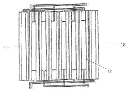
FIG. 1 illustrates the basic geometry of an the MWM sensor 16, a detailed
description
of which is given in U.S. Patents 5,453,689, 5,793,206, and 6,188,218 and U.S.
Patent
Application numbers 09/666,879 and 09/666,524, both filed on September 20,
2000, the
entire teachings of which are incorporated herein by reference. The sensor
includes a primary
winding 10 having extended portions for creating the magnetic field and
secondary windings
12 within the primary winding for sensing the response. The primary winding is
fabricated in
a spatially periodic pattern with the dimension of the spatial periodicity
termed the spatial
wavelength ~,. A current is applied to the primary winding to create a
magnetic field and the
response of the MUT to the magnetic field is determined through the voltage
measured at the
CA 02464586 2004-04-16
-10-
terminals of the secondary windings. This geometry creates a magnetic field
distribution
similar to that of a single meandering winding. A single element sensor has
all of the sensing
elements connected together. The magnetic vector potential produced by the
current in the
primary can be accurately modeled as a Fourier series summation of spatial
sinusoids, with
the dominant mode having the spatial wavelength 7~. For an MWM-Array, the
responses
from individual or combinations of the secondary windings can be used to
provide a plurality
of sense signals for a single primary winding construct as described in U.S.
Patent 5,793,206
and Re. 36,986.
In operation, the drive windings for the sensors are excited with a current at
a
prescribed frequency, for magnetoquasistatic (MQS) inspection of metals. When
interrogating a conducting material, for example, in an aircraft engine disk
slot or bolt hole,
the current in the drive produces a time varying magnetic field that induces
eddy currents in
the material under test. These induced eddy currents within the metal follow
the same path as
the linear drive segments. In other words, the eddy current pattern, induced
in the material
under test, looks like a reflected image of the drive winding geometry. When a
crack,
corrosion damage, an inclusion, surface roughness, local residual or applied
stress change, or
an internal geometric feature alters the flow of these eddy currents, then the
inductive sensing
coils sense an absolute magnetic field that is altered locally by the presence
of the crack, other
damage, or material property variation. The use of absolute inductive sensing
coils, instead
of differential sensing coils, permits the use of models based on physical
principles to analyze
the data. For example, the goal might be to measure the sensor proximity to
the surface,
called the lift-off, at each sensing element and the electrical conductivity
of the material along
the path of the induced eddy currents. A model-based inversion then permits,
for example,
independent conductivity and lift-off measurements. Conventional eddy current
sensors with
absolute or differential elements empirically correct for lift-off instead of
using a physical
model.
Eddy-current sensor arrays comprised of at least one meandering drive winding
and
multiple sensing elements can also be used to inspect the test material.
Example sensor
arrays are shown in FIG. 2 through FIG. 5, FIG. 21, and FIG. 22 and are
described in detail in
CA 02464586 2004-04-16
-11-
U.S. Patent Application number 10/102,620, filed March 19, 2002, the entire
teachings of
which are incorporated herein by reference. This array includes a primary
winding 70 having
extended portions for creating the magnetic field and a plurality of secondary
elements 76
within the primary winding for sensing the response to the MUT. The secondary
elements are
pulled back from the connecting portions of the primary winding to minimize
end effect
coupling of the magnetic field. Dummy elements 74 can be placed between the
meanders of
the primary to maintain the symmetry of the magnetic field, as described in
U.S. Patent
6,188,218. When the sensor is scanned across a part or when a crack propagates
across the
sensor, perpendicular to the extended portions of the primary winding,
secondary elements 72
in a primary winding loop adjacent to the first array of sense elements 76
provide a
complementary measurement of the part properties. These arrays of secondary
elements 72
can be aligned with the first array of elements 76 so that images of the
material properties will
be duplicated by the second array. Alternatively, to provide complete coverage
when the
sensor is scanned across a part the sensing elements, can be offset along the
length of the
primary loop or when a crack propagates across the sensor, perpendicular to
the extended
portions of the primary winding, as illustrated in FIG. 2.
The dimensions for the sensor array geometry and the placement of the sensing
elements can be adjusted to improve sensitivity for a specific inspection. For
example, the
effective spatial wavelength or the distance between the central conductors 71
and the current
return conductor 91 can be altered to adjust the sensitivity of a measurement
for a particular
inspection. For the sensor array of FIG. 2, the distance 80 between the
secondary elements 72
and the central conductors 71 is smaller than the distance 81 between the
sensing elements 72
and the return conductor 91. An optimum response can be determined with
models,
empirically, or with some combination of the two. An example of a modified
sensor design
is shown FIG. 3. In this sensor array, all of the sensing elements 76 are on
one side of the
central drive windings 71. The size of the sensing elements and the gap
distance 80 to the
central drive windings 71 are the same as in the sensor array of FIG. 2.
However, the distance
81 to the return of the drive winding has been increased, as has the drive
winding width to
accommodate the additional elements in the single row of elements. Another
example of a
modified design is shown in FIG. 4. Here, most of the sensing elements 76 are
located in a
CA 02464586 2004-04-16
-12-
single row to provide the basic image of the material properties. A small
number of sensing
elements 72 are offset from this row to create a higher image resolution in a
specific location.
Other sensing elements are distant from the main grouping of sensing elements
at the center
of the drive windings to measure relatively distant material properties, such
as the base
material properties for plates at a lap joint or a weld.
The use of relatively small sensing elements, e.g., down to 1 mm by 1 mm (0.04
in. by 0.04
in.) or smaller squares in an array, permits high resolution imaging of
absolute properties.
High resolution imaging is critical for detection of small cracks, while
absolute imaging is
critical to correct robustly for lift-off variations and to provide reliable
crack responses for
cracks that form in clusters, as is typical for cracks in the fretting regions
of engine disk slots.
In an embodiment, the number of conductors used in the primary winding can be
reduced further so that a single rectangular drive is used. As shown in FIG.
5, FIG. 21, and
FIG. 22, a single loop having extended portions is used for the primary
winding. A row of
sensing elements 75 is placed on the outside of one of the extended portions.
This is similar
to designs described in U.S. Patent 5,453,689 where the effective wavelength
of the dominant
spatial field mode is related to the spacing between the drive winding and
sensing elements.
This spacing can be varied to change the depth of sensitivity to properties
and defects.
Advantages of the design in FIG. 5 include a narrow drive and sense structure
that allows
measurements close to material edges and non-crossing conductor pathways so
that a single
layer design can be used with all of the conductors in the sensing region in
the same plane.
The width of the conductor 91 farthest from the sensing elements can be made
wider in order
to reduce an ohmic heating from large currents being driven through the drive
winding. In
addition, dummy sense elements 89 with substantially portions of the
connection leads can
also be used to help maintain the spatial distribution of conductors around
the sense elements
and to reduce edge effects for the outer elements of the array.
One complication in designing and fabricating the arrays is the need to bring
out
numerous leads from the sensing elements. This can be accomplished using
connection leads
as shown in FIG. 6 where the leads to each sensing element 83 are closely
paralleled by
another set of leads 85 ending in a closed loop 87. This flux cancellation
lead design, as
CA 02464586 2004-04-16
-13-
described in U.S. Patent Application numbers 09/666,879 and 09/666,524, has
the differential
response between the actual sensing element 83 and the parallel leads 85
measured. This lead
design permits direct cancellation of contributions from the leads of the
sensing elements to
the voltage measured at the terminals of these elements. The resulting
capability to use long
leads permits simple and low-cost microfabrication methods and connector
designs to be
used. This, in turn, improves sensor connector durability, while substantially
reducing sensor
replacement costs. In this design the primary windings 70 are separated from
the secondary
element arrays 72 and 76 by a layer of insulation 95. This layer of insulation
is typically 0.5
to 1 mil (12.7 to 25.4 micrometers) thick KaptonTM. The central drive winding
71 can also be
placed on the same side of the insulating layer 95 as the sense elements 72
and 76. Other
similar lead designs might be used on two layers to similarly cancel the flux.
For example,
instead of bringing the flux cancellation leads 85 back on the same layer
along side the sensor
leads 83, they could travel in the second layer on top of the sensor leads
again canceling the
flux contribution from the leads.
The MWM sensor and sensor array structure can be produced using micro-
fabrication
techniques typically employed in integrated circuit and flexible circuit
manufacture. This
results in highly reliable and highly repeatable (i.e., essentially identical)
sensors, which has
inherent advantages over the coils used in conventional eddy-current sensors.
As indicated by
Auld and Moulder, for conventional eddy-current sensors "nominally identical
probes have
been found to give signals that differ by as much as 35%, even though the
probe inductances
were identical to better than 2%" [Auld, 1999] . This lack of reproducibility
with conventional
coils introduces severe requirements for calibration of the sensors (e.g.,
matched
sensor/calibration block sets). In contrast, duplicate MWM sensor tips have
nearly identical
magnetic field distributions around the windings as standard micro-fabrication
(etching)
techniques have both high spatial reproducibility and resolution. The sensor
response can be
accurately modeled which dramatically reduces calibration requirements. For
example,
calibration in air can be used to measure an absolute electrical conductivity
without
calibration standards. The windings are typically mounted on a thin and
flexible substrate,
producing a conformable sensor. The insulating layers can be a flexible
material such as
Kapton~, a polyimide available from E. I. DuPont de Nemours Company.
CA 02464586 2004-04-16
-14-
The single layer designs of the drive and sensing elements supports low cost
fabrication without introducing excessive requirements to align multiple
layers. This
significantly reduces manufacturing costs and increases the number of
suppliers that can
fabricate the sensors. However, to obtain reasonable signal to noise levels
for such single
turn coils (simple rectangles) at low frequencies, it is necessary to apply
more current than is
typical for conventional eddy current sensors, e.g., over 1 A. Fortunately, at
the high
frequencies used for surface-breaking flaws in engine components (e.g., 5 MHz
to 32 MHz),
there is plenty of signal, even for a single turn coil without requiring such
high drive currents.
One practical limitation on the sensing element size is fabrication costs
(e.g., 75 ~m line
widths and larger are low cost with many suppliers, while smaller line widths
is more costly
and limits available suppliers). Another limitation is the relative
contribution to the signal of
the flux coupled by the active sensing area to the flux coupled by the
relatively long leads.
Thus, these leads are kept close together and the novel "flux cancellation"
design is used to
literally cancel the contribution from these Long leads (thus instead of two
conductors entering
each sensing element, there are actually four conductors - two to sense the
flux linked by the
sensing elements and the leads themselves, and the other two to cancel the
contribution from
the leads, leaving just the response of the sensing elements).
For eddy current sensors operating at high frequencies, the induced eddy
currents are
confined to a thin layer (due to the skin effect) near the surface, while at
low frequencies this
layer penetrates deeper into the material under test where it is limited by
the sensor geometry.
For MWM sensors and MWM-Arrays, the depth of penetration of the magnetic field
into the
material under test at lower frequencies is also limited to a fraction of the
drive winding
spatial wavelength, ~,. The depth of penetration of magnetic fields into
titanium or nickel
alloys at higher frequencies is approximately equal to the conventional skin
depth
8=(2/w~a)'~, where w=2~f is the angular frequency for frequency f, p, is the
magnetic
permeability, and ~ is the electrical conductivity. For lower frequencies, the
MWM f eld
depth of penetration for each spatial Fourier mode n is 1/Re(I""), where
kn -E-~C~,uO'= (2a~t~~l,)2 -f-~2~82
CA 02464586 2004-04-16
-15-
k~ 2~n/~, is the spatial mode number, and ~, is the spatial wavelength of the
drive winding
(Goldfine, 1993). The fundamental spatial mode (n=1) has the greatest depth of
penetration,
with a spatial wavelength equal to ~,. This spatial wavelength is taken as two
times the
spacing between the linear drive segments and is similar to that of a coil
with a diameter
approximately equal to the half wavelength. For the same drive current
frequency the
magnetic fields from a longer wavelength (e.g., 16.7 mm) sensor will penetrate
deeper into
the material under test than the fields from a shorter wavelength (e.g., 3.6
mm) sensor. As
shown in FIG. 7, this is true at relatively low frequencies, e.g., under 1 MHz
for titanium or
nickel alloys. Over 10 MHz, the wavelength does not significantly affect the
depth of
penetration of the fields.
For the MWM and MWM-Arrays, the sensor response at each sensing element is
typically obtained in terms of the magnitude and phase (or real and imaginary
part) of the
transinductance. The transinductance is equal to the transimpedance divided by
the angular
frequency, w=2~f, where f is the frequency of the applied drive winding
current. The
transimpedance is the voltage measured at the two terminals of the sensing
elements vS
divided by the applied current id.
transimped ante _ sensing element vo page - v-s
drive winding current i d
For the original MWM sensor of Figure 1 a, the sensing element voltage is the
sum of the
voltages induced on each set of meandering secondaries. The transinductance is
then
transimpe~ce vs
transind~ance= -
.1 ~ .12~a
where j=(-1)'~z. The transinductance has the units of inductance and reflects
the inductive
coupling between the drive winding and sensing elements.
Any model-based nondestructive testing approach requires that the sensor
behavior
match the model predictions for the material under test. Furthermore, to be
practical, each
individual sensor should be essentially identical. The MWM was designed to
provide
CA 02464586 2004-04-16
-16-
responses that matched the behavior of analytical models derived from basic
physical
principles. In contrast, eddy current sensors are typically designed to be
very sensitive and
then the response is modeled without trying to redesign the sensor to reduce
the error between
the actual and predicted response (Dodd, 1982). One benefit of designing the
sensor to match
a model is a simplified calibration procedure. To calibrate, a measurement is
simply
performed in air, away from any conducting or magnetic media. This "air
calibration,"
described in U.S. Patent 6,188,218, corrects for variations in cable
capacitance, unmodeled
inductive coupling and drift in instrumentation. Most importantly, this air
calibration permits
the measurement of absolute electrical properties that are robust and can
reflect, for example,
microstructure of the material under test. These measurements are often
directly comparable
to literature values for the material properties. As part of the calibration,
measurements are
sometimes also performed with a "shunt" sensor that has the connection leads
at the sense
element shorted together. This provides a direct measurement of the parasitic
effect of the
leads on the measurement response. Preferably, the shunt measurement is
performed with the
shunt sensor on the component, or a part with similar properties as the
component, to be
inspected so that the calibration conditions mimic the inspection conditions
as well as
possible. In addition, it is sometimes helpful to perform shunt measurements
both in air and
on the part.
Scanning arrays provide imaging of flaws in metallic components. For example,
MWM-Array images revealed distributed microcracks, small cracks and visible
macrocracks
in an aluminum four-point bending fatigue specimen as described in U.S. Patent
Application
No. 10/345,883. Images can be obtained with the sensor in different
orientations. The
MWM-Array is most sensitive to cracks that are oriented perpendicular to the
linear drive
segments (note that the induced eddy currents are dominantly in the direction
of the longer
linear drive segments). The MWM remains sensitive to cracks oriented as much
as 75
degrees from this perpendicular orientation and even higher in the case of
macrocracks and
EDM notches. EDM notches can be easily detected even when they are parallel to
the drive
windings, which is the disadvantage of EDM notches for demonstrating
sensitivity. Because
they are not as tight as real cracks, they can be detected at all
orientations. Since the array is
sensitive to cracks that are as much as 75 degrees away from the perpendicular
orientation,
CA 02464586 2004-04-16
' 17-
two scans can be performed, with drive winding orientations that differ by at
least 15 degrees,
to detect cracks in all orientations.
Sensor arrays can also be designed to provide measurements at two or more
different
orientations so that a single pass of the sensor array is required, which also
improves
throughput. An example is the sensor design of FIG. 26, which shows a drive
winding 105
configured to provide two different orientation angles when scanned over a
material surface.
One linear array of sense elements 107 are at a different angle than a second
linear array of
sense elements 109, which ensures that all crack orientations are covered.
Deep penetration sensors, which have a longer spatial wavelength, provide the
capability to image hidden geometric features in engine components, measure
wall thickness
in turbine blades, and the ability to manually scan wide areas and build high
resolution
images without expensive scanners. This ability to detect subsurface damage,
demonstrated
for hidden corrosion damage, described in U.S. Patent Application No.
10/345,883, is also
useful for detection of subsurface anomalies in engine disks, such as buried
inclusions.
An efficient method for converting the response of the MWM sensor into
material or
geometric properties is to use grid measurement methods. These methods map the
magnitude
and phase (or real and imaginary parts) of the sensor impedance into the
properties to be
determined and provide for a real-time measurement capability. The measurement
grids are
two-dimensional databases that can be visualized as "grids" that relate two
measured
parameters to two unknowns, such as the electrical conductivity (or magnetic
permeability)
and lift-off (where lift-off is defined as the proximity of the MUT to the
plane of the MWM
windings). For the characterization of coatings or surface layer properties,
three- (or more)-
dimensional versions of the measurement grids called lattices and hypercubes,
respectively,
can be used. Alternatively, the surface layer parameters can be determined
from numerical
algorithms that minimize the error between the measurements and the predicted
responses
from the sensor.
An advantage of the measurement grid method is that it allows for real-time
measurements of
the absolute electrical properties of the material and geometric parameters of
interest. The
CA 02464586 2004-04-16
-18-
database of the sensor responses can be generated prior to the data
acquisition on the part
itself, so that only table lookup operation, which is relatively fast, needs
to be performed.
Furthermore, grids can be generated for the individual elements in an array so
that each
individual element can be lift-off compensated to provide absolute property
measurements,
such as the electrical conductivity. This again reduces the need for extensive
calibration
standards. In contrast, conventional eddy-current methods that use empirical
correlation
tables that relate the amplitude and phase of a lift-off compensated signal to
parameters or
properties of interest, such as crack size or hardness, require extensive
calibrations and
instrument preparation. A representative measurement grid for a low-
conductivity
nonmagnetic metal (e.g., titanium alloys, some superalloys, and austenitic
stainless steels) is
illustrated in FIG. 8.
FIG. 9 shows an example of a measurement grid used to estimate the
conductivity and
lift-off for a high conductivity nonmagnetic metal (e.g., aluminum alloy). In
this case, the
model assumed that the material under test (MUT) was an infinite half space
(i.e., a single
layer of infinite thickness). This is a reasonable assumption when the skin
depth is small
compared to the actual thickness of the material under test (as for an engine
disk slot). It also
assumed an air gap (or insulating layer) exists between the sensor and the
first conducting
surface. This "air gap" is called the lift-off. The data shown in FIG. 9 is
for a single channel
(sensing element) of an MWM-Array as it is scanned across a surface. For more
complicated
problems, such as a crack under a coating on a turbine blade, the two unknowns
might be the
lift-off and the conductivity of the substrate, using a three-layer model
(i.e., the lift-off gap is
one layer, the coating is a second layer, and the substrate is a third,
infinitely thick layer).
Alternatively, two or more frequencies can be used with mufti-dimensional
databases (e.g.,
lattices or hypercubes) to estimate more than two unknown properties.
A typical frequency used in single frequency measurements of engine disk slots
is 6.3 MHz.
This frequency is sufficient for detection of the 1.5 mm (0.06 in.) long
cracks. However, for
smaller cracks in other more critical locations operation at significantly
higher frequencies
may be required. For crack detection and length, location, and depth
determination multiple
frequency methods can be used.
For measuring the response of the individual sensing elements in an array,
CA 02464586 2004-04-16
-19-
multiplexing between the elements can be performed. However, this can
significantly reduce
the data acquisition rate so a more preferably approach is to use an impedance
measurement
architecture that effectively allows the acquisition of data from all of the
sense elements in
parallel. To perform absolute measurements of material properties, to robustly
correct images
for lift-off variations caused by varying surface roughness and curvature, and
to develop
reliable multiple frequency crack response signals, it is essential to
generate robust impedance
data across multiple frequencies and across wide ranges of impedance magnitude
and phase.
This type of instrument is described in detail in U.S. Patent Application
number 10/155,887,
filed May 23, 2002, the entire teachings of which are incorporated herein by
reference. This
instnunentation can acquire data from 39 fully parallel impedance channels
(magnitude and
phase) simultaneously in less than 10 milliseconds (e.g., 100 measurements per
second on 39
channels simultaneously). This speed is critical for increasing throughput
rates for inspection
of wide areas such as the entire internal surface of an engine disk slot, or a
bore, a web region,
or a high aspect ratio bolt hole in an engine disk. To perform measurements
with the grid
methods and air calibration, each channel must provide a robust and accurate
measurement of
absolute impedance. The use of multiple sensing elements with one meandering
drive and
parallel architecture measurement instrumentation then permits high image
resolution in real-
time.
FIG. 10 provides an illustration of an MWM-Array probe configured for slot
inspection. The flexible MWM-Array 30 is placed in the slot 44 of the disk 42
with a support
32. The support can be rigid or can include conformable components such as an
inflatable
balloon as described in U.S. Patent Application No. 10/172,834, filed June 13,
2002, the
entire teachings of which are incorporated herein by reference. The inflatable
balloon can be
filled with water to provide pressure behind the sensor and can improve sensor
durability (i.e.,
by deflating the balloon prior to entry into the slot). The support 32 can be
attached to probe
electronics 34, which provide amplification of the sense element signals, a
shaft 36, which
guides the scan direction for the sensor, and a balloon inflation mechanism
38. A position
encoder 40 provides longitudinal registration of the MWM-Array data along the
axis of the
inspected slot. The sensing elements positions (with 0.04 in. spacing) provide
the position in
the transverse direction, resulting in a fully registered two-dimensional
image, with manual
CA 02464586 2004-04-16
-20-
scanning using an single, axial, position encoder. The electrical signals are
monitored with
the parallel architecture data acquisition impedance instrumentation 46
through electrical
connections from the probe electronics 45 and the position encoder 43. A
connection 47
between the impedance instrument and a processor 48, such as a computer, is
used to control
the data acquisition and process and display the data.
This probe has the capability to inspect both the lower and upper quadrant of
the slot
on one side in a two step process. The process involves manually pressing a
button that
conveniently and quickly shifts the encoder configuration to support scanning
the bottom
quadrant of the slot side beginning at the center and then returning to the
center, pressing the
button, and scanning the upper quadrant of the slot side. This design requires
the operator to
flip over the disk to then inspect the upper and lower quadrants of the
opposite side of the
slots. Alternatively, the MWM-Array can be designed to permit scanning of both
sides
simultaneously, without flipping over the engine disk, permitting rapid
scanning of both sides
in either a manual or automated operation. 'The use of balloons that are
deflated upon entry
into the slot often extends the life of the sensors by limiting damage upon
entry into the slot.
Also, combinations of balloons and foam with plastic can often improve
conformability to
complex slot geometries.
FIG. 11 and FIG. 12 provide typical conductivity images obtained from engine
slots with
fretting damage. Slots 2 through 9 of this F-I 10 engine disk were selected
because they
contain several cracks in the range from 0.38 mm (0.015-in.) to 5.1 mm (0.20-
in.), with six
documented cracks under 2.5 mm (0.1-in.) based on acetate replicas. In this
case, the
objective was to reliably detect cracks I .5 mm (0.06-in.) and longer with
reasonable false
alarm rates. As shown in FIG. 11 and FIG. I2, cracks I .25 mm (0.05-in.) and
longer provide
large indications easily visualized in the two-dimensional images (C-scans)
with no
background indications even approaching their signal level. The two smaller
cracks 0.9 mm
(0.035-in.) long in slot 5 and I .0 rnm (0.04-in.) long in slot 9 produce
significant signals,
however, these are well below the required detection threshold so no attempt
was made to
enhance their detection. The single frequency measurements shown here may
produce false
positive indications if the smaller crack images are enhanced.
CA 02464586 2004-04-16
-21-
Two processing steps were performed on the MWM-Array transinductance data. The
first was to convert the transinductance real and imaginary parts into
absolute electrical
conductivity and lift-off images using the grid measurement methods. The
resulting
conductivity images are then corrected for lift-off variations away from the
cracks. However,
since the cracks themselves were not modeled in this case, the lift-off
correction at the crack
location is not an exact correction. The second processing step was to
normalize the response
by adjusting each sense element. The adjustment may involve dividing each
sense element
response by the average response for each element where the average is taken
over a specified
area within the slot that does not contain a crack. The response may then be
rescaled (e.g.,
multiplied) by the average response for all of the sense elements or a
specified value. The
adjustment may also involve subtraction of the average response or some other
pre-selected
level. The images are then presented with a color scale selected intentionally
to emphasize
cracks longer than 1.25 mm (0.05-in.) and to suppress smaller cracks and
background
variations.
As another alternative, other crack signature enhancement tools can also be
applied.
For example, as described in U.S. Patent Application No. 10/345,883, filed
January 15, 2003,
the entire teachings of which are incorporated herein by reference, a
combination of multiple
frequencies and spatial matched filters can enhance the crack responses and
suppress clutter
(non-crack like background signals). This would improve detection thresholds
but may limit
robustness to certain types of cracks. Care must be taken when "optimizing"
detection filters
on a specific training set or even test set of cracks that may not completely
represent the
population of possible cracks in service run hardware.
For the images of FIG. 1 l and FIG. 12, a calibration was performed in air
with no
calibration standards. At overhaul facilities, detection thresholds would be
set based on
results obtained from a training set of actual disk specimens with real cracks
ideally formed in
service. Calibration takes approximately 15 seconds, not including initial
system warm-up
and setup time of about fifteen minutes. Scans take less than one minute per
slot. The
elimination of expensive scanners and the increase in throughput compared to
single coil
inspection methods (that typically take 10 to 20 minutes per slot) offer
substantial cost
CA 02464586 2004-04-16
-22-
savings potential.
Another feature evident in the scan images of, for example, FIG. 11 is the
flange at the
edge of the slot. FIG. 13 provides an expanded view of the edge signature. The
effective
width of this edge is less than 0.5 mm (0.02-in.) in the lift-off corrected
conductivity images.
Thus, for F-110 engine disks the capability to reduce the edge signature to
less than 0.5 mm
(0.02-in.) combined with the capability to detect cracks longer than 1.0 mm
(0.04-in.)
satisfies the inspection requirement for detecting cracks longer than 1.5 mm
(0.06-in.) within
the slot. This capability to minimize the edge signature results from both the
small sensing
element size and the use of the balloon to provide even and consistent
pressure on the MWM-
Array sensing elements as the sensor moves off the edge.
FIG. 14 though FIG. 17 provide the corresponding individual channel (sensing
element) responses (B-scans) for slots 2, 5, and 9 in one of the disks. Only
the response from
the channel that passes over the crack is plotted. Repeated measurements
within these slots
continually produce similar results. Even the background variations appear
repeatable. In
Slot 9 there are two significant crack indications as shown in FIG. 17.
Figure 9a shows a plot of the estimated crack length compared to the actual
crack length
determined from acetate replicas taken in the slots, as described earlier.
Figure 9b provides a
similar plot of the estimated distance from the slot edge to the nearest tip
of the first crack
detected within the slot.
The effective property measurements made with the MWM-Array can also be used
to
determine the crack length and location within the slot. As a demonstration of
this capability,
the 1.25 mm (0.05-in.) long crack in slot 2 was used as the training set. As
shown in FIG. 14,
the width of the crack response at a specific percentage of the normalized
conductivity
response was used to estimate the crack length. The percentage of the response
height at
which the width of the crack response matched the documented crack length for
the training
set crack was used. In this case, the response width matched the length of the
1.25 mm (0.05-
in.) long crack at sixty percent (60%) of the response height. Note that this
is a simple
example and several cracks could be used in the training set, but setting this
percentage this
CA 02464586 2004-04-16
-23-
would not have to be performed at each inspection; it would be performed only
once for a
given sensor and inspection application. Thus, the response width at 60% of
the response
height was used to estimate the length of the other cracks in the eight
inspected slots. FIG. 18
shows the crack length estimation results for these cracks. A relatively
linear response exists
for the six documented cracks in these eight slots. The longest crack at 5.0
mm (0.2-in.) was
actually comprised of a principal crack about 4.1 mm (0.16-in.) long, which
agrees well with
the MWM response, and a very tight extension of this crack that is only
visible under a
microscope. Consequently, this crack is indicated here by two symbols. The 1.0
mm (0.04
in.) crack in slot 9 is slightly out of line. This crack was between the
larger crack and another
apparent crack slightly farther into the slot that was not completely
documented with acetate
replicas. The crack may have actually been longer than determined from the
replica if, for
example, there was a tight extension as with the 5.0 mm (0.2-in.) long crack
in the same slot.
FIG. 19 provides the crack location in terms of the distance from the slot
edge to the
nearest tip of the first crack detected within the slot. The agreement here is
more consistent
because the effect of "tight extended cracks" over these longer distances is
less apparent than
on shorter distances for the crack length plot of FIG. 18. The two-dimensional
images clearly
indicate the edge and illustrate the high resolution imaging capability of the
MWM.
As another alternative embodiment, in addition to inductive coils, other types
of
sensing elements, such as Hall effect sensors, magnetoresistive sensors,
SQUIDS, and giant
magnetoresistive (GMR) sensors, can be used in place of, or in combination
with, inductive
coils. The use of GMR sensors for characterization of materials is described
in more detail in
U.S. Patent Application numberl0/045,650, the entire teachings of which are
hereby
incorporated by reference.
As a validation of sensor performance, an MWM-Array was used to perform a
limited
POD study on titanium alloy ENSIP flat specimens. The flat specimens were
selected by an
original equipment manufacturers (OEM) to be representative of the ENSIP flat
specimens
used in other POD studies. For this study, a two-frequency method (8 and 12
MHz) was
used. Reducing the sensing element footprint and using more (e.g., three) and
higher (up to
CA 02464586 2004-04-16
-24-
32 MHz) frequencies can improve sensitivity for smaller cracks.
The results of the POD study with comparisons of the MWM-Array results to (1)
a
standard eddy current sensor and (2) an OEM conformable eddy current array
(both with
differential coil designs) are provided in FIG. 20. The ENSIP flat specimens
used in this
study were selected to demonstrate relative detection capability. A set of
fourteen ENSIP Ti 6-
4 specimens containing six cracks each were used for initial testing. The
crack length in this set
varied from 0.1 to 1.5 mm (0.004 to 0.058-in.). Four specimens containing 23
cracks were
selected by the OEM for blind tests at the OEM facility.
The MWM-Array results shown here are for three different detection threshold
settings. The
false alarm rate for the MWM, in each case, is less than S%. When comparing
probability of
detection performance, care should be taken to set false alarm rates at
identical levels.
Robust comparison of different technologies requires detailed knowledge of
each method's
detection algorithms and all recorded false alarms. For example, if a larger
footprint sensor is
compared to a smaller footprint sensor, there is inherent averaging with the
larger sensor that
may reduce the number of false alarm opportunities. This would require the
false alarm rates
to be scaled accordingly to provide a fair POD comparison. Since this is not
common
practice, only general conclusions can be drawn from such limited POD studies.
The false
alarm information was not available in this for all sensors tested.
Nevertheless, the results of
the limited POD study presented in FIG. 20 demonstrate representative
inspection reliability
for the MWM-Array.
The lack of available fabricated test specimens with simulated or real cracks
in
regions with fretting damage makes qualification of NDE methods using accepted
POD study
methods difficult. One approach, however, is to use a substantial set of
available specimens
with real cracks from service-run hardware that has been removed from service
after
detection of cracks. Fortunately, for the specific engine disks addressed
herein, there is a
substantial supply of such service-run disks. Also, disks that have large
cracks tend to have
some smaller cracks as well. The result is a substantial population of slots
with cracks and
slots with no cracks with varying degrees of fretting damage. While it is
important to use
actual field-induced damage for inspection reliability demonstrations,
whenever possible, to
CA 02464586 2004-04-16
-25-
accurately represent crack morphology, local geometry, and surface conditions
such as
fretting, it is important to recognize that there is a potential for cracks to
exist in this
hardware that are not detected by any present nondestructive techniques.
Surface roughness can be measured as well using the relationship between lift-
off and
RA. This is described in the NASA Phase II final report titled "Nondestructive
Characterization of Thermal Spray Coating Porosity and Thickness", dated
September 17,
1997 and in U.S. Provisional Application number 60/065,545, filed November 14,
1997, the
entire teachings of which are incorporated herein by reference. This lift-off
image/data can be
thresholded or analyzed to accept or reject disks based on fretting damage.
Furthermore, the
lift-off level can be used to adjust confidence levels for crack detection
since sensitivity to
cracks is reduced as lift-off increases.
For nickel alloy engine materials, such as Alloy 738 or Alloy 718, shot
peening and/or
heat treatment may produce near surface relative permeability greater than
1Ø FIG. 23
shows a schematic plot relating the relative magnetic permeability to the
compressive and
tensile stresses in the material. The nominal variation of the magnetic
permeability with
depth is illustrated in FIG. 24 and indicates the region of higher
permeability near the surface
caused by the shot peening and/or heat treatment process. FIG. 25 shows the
corresponding
variation in the relative permeability measurement as a function of frequency.
At sufficiently
high frequencies, the magnetic field is confined near the surface of the MUT
and reflects only
the permeability (and stress) of the surface region. At lower frequencies, the
magnetic field
can penetrate through this region and the average or effective permeability is
reduced. At
sufficiently low frequencies, the magnetic field penetrates far enough into
the base material
that the permeability approaches 1Ø High resolution images of permeability
can then be
used to map residual stress variations to qualify shot peening or other
manufacturing
processes or to assess material aging / material degradation, as described in
more detail in
U.S. Patent Application No. 10/351,978, filed January 24, 2003, the entire
teachings of which
are incorporated herein by reference. Then, regions with unacceptable residual
stresses might
be reworked (e.g., blending and reshot peening) to extend life.
CA 02464586 2004-04-16
-26-
While the inventions have been particularly shown and described with reference
to
preferred embodiments thereof, it will be understood to those skilled in the
art that various
changes in form and details may be made therein without departing from the
spirit and scope
of the invention as defined by the appended claims.
References incorporated by reference in their entirety:
Auld, B.A. and Moulder, J.C. (1999), "Review of Advances in Quantitative Eddy-
Current
Nondestructive Evaluation," Journal of Nondestructive Evaluation, vol. 18, No.
1.
Dodd, C., and W. Deeds (1982), "Absolute Eddy-Current Measurement of
Electrical
Conductivity," Review of Progress in Quantitative Nondestructive Evaluation,
Vol. 1, 1982.
Plenum Publishing Co.
Goldfine, N. (1993), "Magnetometers for Improved Materials Characterization in
Aerospace
Applications," Materials Evaluation Vol. 51, No. 3, pp. 396-405; March 1993.
MIh-HDBK-1823 (1999), "Nondestructive Evaluation System Reliability
Assessment,"
Department of Defense Handbook, 30 April 1999.
The following references are also incorporated herein by reference in their
entirety.
NASA Phase II Praposal, titled "Shaped Field Giant Magnetoresisitive Sensor
Arrays for
Materials Testing," Topic #O1-II A1.05-8767, dated May 2, 2002
Navy Phase I Proposal, titled "Observability Enhancement and Uncertainty
Mitigation for
Engine Rotating Component PHM," Topic #N02-188, dated August 14, 2002.
NASA Phase I Proposal, titled "Non-Destructive Evaluation, Health Monitoring
and Life
Determination of Aerospace Vehicles/Systems," Topic #02-H5.03-8767, dated
August 21,
2002.
CA 02464586 2004-04-16
-27-
Final Report submitted to FAA, titled "Crack Detection Capability Comparison
of JENTEK
MWM-Array and GE Eddy-current Sensors on Titanium ENSIP Plates", dated
September 28,
2001, Contract #DTFA03-00-C-00026, option 2 CLIN006 and 006a.
NASA Phase II Final Report, titled "Nondestructive Characterization of Thermal
Spray
Coating Porosity and Thickness", dated September 17, 1997, Contract #NASS-
33212.
Technical paper titled "Residual and Applied Stress Estimation from
Directional Magnetic
Permeability Measurements with MWM Sensors," published in ASME Journal of
Pressure
Vessel Technology, Volume 124, pp 375-381; August 2002.
Technical paper titled "Fatigue and Stress Monitoring Using Scanning and
Permanently
Mounted MWM-Arrays," presented at 29th Annual Review of Progress in QNDE;
Bellingham, Washington; July 2002.
Technical paper titled "Absolute Electrical Property Imaging using High
Resolution
Inductive, Magnetoresistive and Capacitive Sensor Arrays for Materials
Characterization,"
presented at 1 lt" International Symposium on Nondestructive Characterization
of Materials,
Berlin, Germany; 3une, 2002.
Technical paper titled "Application of MWM~ Eddy- Current Technology during
Production
of Coated Gas Turbine Components," presented at 11'" International Symposium
on
Nondestructive Characterization of Materials, Berlin, Germany; June 2002.
Technical presentation slides "Condition Assessment of Engine Component
Materials Using
MWM-Eddy-current Sensors," ASNT Fall Conference, Columbus, OH; Oct. 2001.