Note: Descriptions are shown in the official language in which they were submitted.
CA 02473223 2004-07-23
WO 03/065417 PCT/US03/03203
CHARGE CONTROLLED AVALANCHE PHOTODIODE AND METHOD OF
MAKING THE SAME
FIELD OF THE INVENTION
[0001] The present invention relates generally to the field of semiconductor-
based photodetectors, and more specifically to an optimized avalanche
photodiode
and a method of making the same.
BACKGROUND AND SUMMARY OF THE INVENTION
[0002] Owing to the known interaction between photons and electrons, great
advances have been made in the field of photodetectors in recent years,
particularly
in those photodetectors that utilize semiconductor materials. One type of
semiconductor-based photodetector is termed an avalanche photodiode, or APD.
This type of structure is generally composed of a number of solid
semiconductive
materials that serve different purposes such as absorption and multiplication.
[0003] The APD structure provides the primary benefit of large gain through
the action of excited charge carriers that produce large numbers of electron-
hole
pairs in the multiplication layer. However, an APD is so efficient at
producing large
numbers of charge carriers that it runs the risk of becoming saturated, thus
adversely affecting the bandwidth of the device. In order to prevent charge
carrier
breakdown, it is imperative that the electric field be regulated within the
APD itself,
and in particular it is desirable to have the electric field in the
multiplication layer be
significantly higher than that in the absorption layer.
[0004] Traditionally, a separate absorption, grading, charge, multiplication
(SAGCM) APD utilizes a grading layer to minimize hole trapping at the
1
CA 02473223 2004-07-23
WO 03/065417 PCT/US03/03203
heterojunction interface and a charge control layer to separate the electric
field
between the absorption and the multiplication layers. Design of this charge
control
layer is extremely critical in that it should allow for a high enough electric
field
strength to initiate impact ionization in the multiplication layer while
keeping the
electric field in the absorption layer low in order to prevent tunneling
breakdown.
[0005] For example, an SAGCM APD structure with an n-type multiplication
layer, electrons are 'multiplied and a p-type doping is required to act as the
charge
control layer. However, a conventional beryllium or zinc p-type doping method
requires a relatively thick charge control layer because of the high diffusion
coefficient associated with beryllium and zinc. Due to this thick charge
control
region with lower doping, the carrier transit time across the charge control
layer is
increased, thereby reducing the overall speed of these APD devices.
[0006] By way of comparison, in the present invention the limitations manifest
in a beryllium or zinc charge control layer are overcome by utilizing carbon
doping.
This solution results in an ultra-thin charge control layer while increasing
the speed
of the photodetector. Since carbon has a very small diffusion coefficient, a
precise
doping control can be achieved to realize a charge sheet within an ultra-thin
layer of
100 angstroms or less.
[0007] The present invention includes an epitaxial structure grown on a semi-
insulating InP substrate. First, a buffer layer is grown to isolate defects
originated
from substrates. Then an n-type layer is grown to serve as n-contact layer to
collect
electrons. Next, a multiplication layer is grown to provide avalanche gain for
the
APD device. Following that, an ultra-thin charge control layer is grown with
carbon
doping. An absorption layer is grown to serve as the region for creating
electron-
2
CA 02473223 2004-07-23
WO 03/065417 PCT/US03/03203
hole pairs due to a photo-excitation. Finally, a p-type layer is grown to
serve as p-
contact layer to collect holes. Further embodiments and advantages of the
present
invention are discussed below with reference to the Figures.
BRIEF DESCRIPTION OF THE DRAWINGS
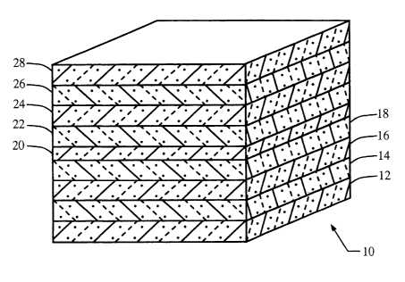
[0008] Figure 1 is a perspective view of a charge controlled avalanche
photodiode in accordance with one aspect of the present invention.
[0009] Figure 2 is a graph depicting the spatial dependence of an electric
field
placed across the depth of a charge controlled avalanche photodiode.
DETAILED DESCRIPTION OF THE PREFERRED EMBODIMENT
[0010] In accordance with a preferred embodiment of the present invention,
an epitaxial structure is provided for photoconductive purposes. The
photoconductive structure is an avalanche photodiode (APD) that is optimized
for
increased performance through a charge control layer. The particulars of the
structure and method of manufacture of the present invention are discussed
further
herein.
[0011] Referring to Figure 1, a perspective view of a charge controlled APD
is shown in accordance with the preferred embodiment. A substrate 12 is
provided as a base upon which the epitaxial structure is deposited. The charge
controlled APD 10 of the present invention may be manufactured in a number
suitable fashions, including molecular beam epitaxy and metal organic vapor
phase
epitaxy.
[0012] The substrate 12 may be composed of a semi-insulating material or
alternatively the substrate may be doped Indium Phosphate (InP). A buffer
layer 14
3
CA 02473223 2004-07-23
WO 03/065417 PCT/US03/03203
is disposed above the substrate 12 to isolate any structural or chemical
defects of
the substrate 12 from the remaining structure.
[0013] An n-type layer 16 is disposed upon the buffer layer 14 to serve as an
n-contact layer and thus collect electrons cascading through the charge
controlled
APD 10. The n-type layer may be composed of one of Indium Phosphate (InP) or
Indium Aluminum Arsenide (InAIAs). Disposed upon the n-type layer 16 is a
multiplication layer 18 composed of InAIAs. The multiplication layer 18
provides the
avalanche effect in which the current density of the electrons is amplified,
thereby
providing the APD gain.
[0014] , A charge control layer 20 is disposed upon the multiplication layer
18
in order to isolate the multiplication layer 18 from the top layers of the
charge
controlled APD 10. In the preferred embodiment, the charge control layer 20 is
composed of carbon-doped InAIAs. The charge control layer 20 is deposited only
to
a thickness of less than 100 angstroms. It is possible that the charge control
layer
20 could be as few as 2 angstroms in thickness, thus representing a two-
dimensional charge sheet. Preferably, therefore, the charge control layer 20
between 2 and 100 angstroms in thickness.
[0015] Two digital graded layers 22, 26 are disposed beneath and above an
absorption layer 24 in order to minimize any carrier trapping due to the
bandgap
between Indium Gallium Arsenide (InGaAs) and InAIAs materials. The first
digital
graded layer 22 is disposed upon the charge control layer 20. The absorption
layer
24 utilized for creating electron-hole pairs is disposed upon the digital
graded layer
22. The second digital graded layer 26 is then disposed upon the absorption
layer
24.
4
CA 02473223 2004-07-23
WO 03/065417 PCT/US03/03203
[0016] In the preferred embodiment, both the first and the second digital
graded layers 22, 26 are composed of Indium Aluminum Gallium Arsenide
(InAIGaAs). The absorption layer 24 is composed of InGaAs in order to maximize
the number of electron-hole pairs produced through photo-excitation.
[0017] A p-type layer 28 serving as a p-contact layer is disposed on the
second digital graded layer 26 in order to collect holes in a manner analogous
to the
n-type layer 16. The p-type layer 26 is preferably one of InP or InAIAs, as
described
above for the n-type layer 16. In related embodiments, the p-type layer 28 and
the
n-type layer 16 may be of the same material, or alternatively, they may be
composed
of differing materials within the set of InP or InAIAs.
[0018] The charge controlled APD 10 described with reference to Figure 1
provides much improved performance over a typical epitaxial APD. In
particular, the
charge control layer 20 is particular adept at maintaining a high electric
field in the
multiplication layer 18 while maintaining a low electric field in the
absorption layer
24.
[0019] Figure 2 is a graph representative of electric field values measured
for
dependency upon depth in the charge controlled APD 10 against various voltage
biases. In particular, it is notable that the absorption layer 24 is typically
disposed
between 0.25 and 1.25 pm from the surface of the p-type layer 28. Similarly,
the
multiplication layer 18 may be disposed between 1.25 and 1.75 pm from the
surface
of the p-type layer 28.
[0020] Accordingly, it is evident from Figure 2 that the charge control layer
20,
disposed between the absorption layer 24 and the multiplication layer 18, is
responsible for a increase in the electric field between the respective
layers. In
CA 02473223 2004-07-23
WO 03/065417 PCT/US03/03203
particular, for a -5V bias, the electric field in the absorption layer 24 is
approximately
zero, whereas the electric field in the multiplication layer 18 is on the
order of -1.75 x
103 V/cm. For a voltage of -30 volts, the electric field in the absorption
layer 24 is
approximately -1.0 x 10³, whereas the electric field in the multiplication
layer 18 is on
the order of -5.0 x 10³ V/cm. Moreover, as the thickness of the charge control
layer
20 is less than 100 angstroms, it also provides substantially decreased
carrier transit
time, resulting in overall efficiencies in the APD response time.
[0021] As described, the present invention consists of an avalanche
photodiode having a charge control layer. In particular, the charge control
layer is
carbon-doped and less than 100 angstroms in thickness, thereby providing an
increased electric field gradient between the absorption and multiplication
layers of
the device. It should be apparent to those skilled in the art that the above-
described
embodiments are merely illustrative of but a few of the many possible specific
embodiments of the present invention. Numerous and various other arrangements
can be readily devised by those skilled in the art without departing from the
spirit and
scope of the invention as defined in the following claims.
6