Note: Descriptions are shown in the official language in which they were submitted.
CA 02474556 2004-07-26
WO 03/065416
PCT/US03/03181
ENHANCED PHOTODETECTOR
FIELD OF THE INVENTION
[0001] The present invention relates to a semiconductor-based
photodetector,
and in particular to a high-speed, broad bandwidth photodetector having
enhanced
absorption characteristics.
BACKGROUND AND SUMMARY OF THE INVENTION
[0002] There is a well-known tradeoff between high speed and sensitivity in
a
photodetector. High bandwidth signal detection requires a short transit time
of the
carriers and thus a thin absorption layer. However, the geometrical
constraints on
the absorption layer thickness results in a reduced absorption and lower
responsivity.
[0003] One type of semiconductor-based photodetector is termed a p-i-n
junction diode, or a PIN diode. This type of structure is generally composed
of a
number of solid semiconductive sandwiched together in an epitaxial structure.
In
particular, a p-type semiconductor material and an n-type semiconductor region
are
separated by an intrinsic semiconductor.
[0004] In a PIN diode, the depletion layer extends into each side of
junction by
a distance that is inversely proportional to the doping concentration. Thus,
the p-i
depletion layer extends well into the intrinsic material, as does the
depletion layer of
the i-n junction. Accordingly, a PIN diode functions like a p-n junction with
a
depletion layer that encompasses the entirety of the intrinsic material. The
primary
advantages inherent to this structure are twofold. First, the addition of the
intrinsic
I
CA 02474556 2004-07-26
WO 03/065416
PCT/US03/03181
layer permits a fractional increase in the amount of light to be captured by
the diode.
Secondly, due to the extended depletion layer, the PIN diode has a very small
junction capacitance and corresponding fast response.
[0005] Most attempts at increasing the speed of PIN diodes have focused on
reducing the capacitance at the junction. At least one proposed design has
included
an undoped drift region for this purpose, effectively increasing the size of
the intrinsic
portion of the diode. Although this solution is suitable for decreasing the
junction
capacitance, it unfortunately increases the transit time for the carriers and
thus
reduces the response time of the photodetector. As such, there is a need in
the art
for an improved photodetector that strikes the proper balance between
capacitance
and response time, while increasing the responsivity of the device.
[0006] Accordingly, the present invention includes a photodiode having a
first
p¨type semiconductor layer and an n-type semiconductor layer coupled by a
second
p-type semiconductor layer. The second p-type semiconductor layer has graded '
doping along the path of the carriers. In particular, the doping is
concentration
graded from a high value near the anode to a lower p concentration towards the
cathode. By grading the doping in this way, an increase in absorption is
achieved,
improving the responsivity of the device. Although this doping increases the
capacitance relative to an intrinsic semiconductor of the same thickness, the
pseudo
electric field that is created by the graded doping gives the electrons a very
high
velocity which more than compensates for this increased capacitance. Further
embodiments and advantages of the present invention are discussed below with
reference to the figures.
2
CA 02474556 2011-06-14
[0006.1] In accordance with one aspect of the present invention, there is
provided a photodiode comprising: a semi-insulating substrate layer; a first p-
type
semiconductor layer; an n-type semiconductor layer; and a second p-type
semiconductor layer disposed between the first p-type semiconductor layer and
the
n-type semiconductor layer such that the second p-type semiconductor is
directly
adjacent to the n-type semiconductor, the second p-type semiconductor layer
having a graded doping concentration along the path of the carriers.
[0006.2] In accordance with another aspect of the present invention, there
is
provided a photodiode comprising: a first p-type semiconductor layer; an n-
type
semiconductor layer; and a second p-type semiconductor layer disposed between
the first p-type semiconductor layer and the n-type semiconductor layer such
that
the second p-type semiconductor is directly adjacent to the n-type
semiconductor,
the second p-type semiconductor layer having a graded doping concentration,
the
graded doping concentration defining a first concentration adjacent to the
first
p-type semiconductor layer and a second concentration adjacent to the n-type
semiconductor layer, the first concentration being greater than the second
concentration, and the first concentration being located at a position xo and
defining a concentration po, and the graded doping concentration being
governed
by the following equation:
-x
p = p oe
2a
CA 02474556 2011-06-14
over the depth D of the second p-type semiconductor layer for all x and D
greater
than zero.
[0006.3] In
accordance with a further aspect of the present invention, there is
provided a method of fabricating a photodiode comprising: providing a
substrate
layer; depositing an n-type semiconductor layer on the substrate; depositing a
second p-type semiconductor layer having a p-type dopant on the n-type
semiconductor layer; grading the p-type dopant of the second p-type
semiconductor layer from a first concentration to a second concentration,
wherein
the first concentration is greater than the second concentration; and
depositing a
first p-type semiconductor layer on the second p-type semiconductor layer,
wherein
the second p-type semiconductor layer is between the first p-type
semiconductor
layer and the n-type semiconductor layer such that the second concentration is
directly adjacent to the n-type semiconductor layer, and wherein the first
concentration is located at a position xo and defines a concentration po, and
further
wherein the graded doping concentration is governed by the following equation:
-x
p = p
over the depth D of the second p-type semiconductor layer for all x and D
greater
than zero.
2b
CA 02474556 2011-06-14
[0006.4] In
accordance with yet a further aspect of the present invention, there
is provided a photodiode having a first p-type semiconductor layer and an n-
type
semiconductor layer comprising: a second p-type semiconductor layer disposed
between the first p-type semiconductor layer and the n-type semiconductor
layer
such that the second p-type semiconductor is directly adjacent to the n-type
semiconductor, the second p-type semiconductor layer having a graded doping
concentration, wherein the graded doping concentration is governed by the
following equation:
-x
p= poet'
over the depth D of the second p-type semiconductor layer for all x and D
greater
than zero.
2c
CA 02474556 2004-07-26
WO 03/065416
PCT/US03/03181
BRIEF DESCRIPTION OF THE DRAWINGS
[0007] Figure 1 is an energy band diagram of a pin photodiode in
accordance
with the present invention.
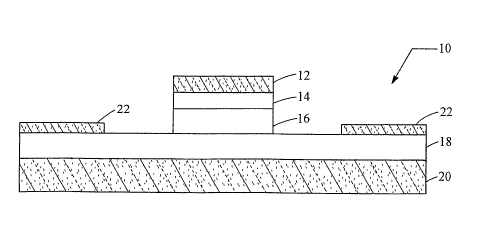
[0008] Figure 2 is a cross-sectional view of a basic configuration of a
pin
photodiode in a surface illuminated structure in accordance with the present
invention.
[0009] Figure 3 is a graph representing the relationship between the
electric
field and the electron velocity according to an aspect of the present
invention.
[0010] Figure 4 is a graph representing the relationship between the
doping
concentration and the relative depth of a semiconductor layer of the present
invention.
DETAILED DESCRIPTION OF THE PREFERRED EMBODIMENT
[0011] In accordance with a preferred embodiment of the present invention,
an epitaxial structure is provided for photoconductive purposes. The
photoconductive structure is a modified PIN diode that is optimized for
increased
performance through an enhanced layer having a graded doping concentration.
The
particulars of the structure and method of manufacture of the present
invention are
discussed further herein.
[0012] Referring to Figure 1, an energy band diagram of a PIN photodiode
10
shows the relative energy revels of the semiconductor materials that form the
photodiode 10. In particular, the photodiode 10 is comprised of a group of
semiconductor materials, including a first p-type semiconductor layer 14, a
second
p-type semiconductor layer 16, and an n-type semiconductor layer 18. An anode
layer 12 is shown adjacent to the first p-type semiconductor layer 14 to
collect holes.
3
CA 02474556 2004-07-26
WO 03/065416
PCT/US03/03181
[0013] The first p-type semiconductor layer 14 is selected from a group
comprising tertiary semiconductors, or group 111-V semiconductors.
Accordingly, the
first p-type semiconductor layer 14 is either two elements from group III
combined
with one element from group V or the converse, two elements from group V
combined with one element from group III. A table of representative groups of
the
periodic table is shown below.
GROUP II GROUP Ill GROUP IV GROUP V
Zinc (Zn) Aluminum (Al) Silicon (Si) Phosphorus (P)
Cadmium (Cd) Gallium (Ga) Germanium (Ge) Arsenic (As)
Mercury (Hg) Indium (In) Antimony (Sb)
[0014] In the preferred embodiment, the first p-type semiconductor layer 14
is
InAlAs. However, it is understood that the first p-type semiconductor layer 14
may
be any tertiary semiconductor that provides the necessary bandgap for
optimized
operation of the photodiode 10.
[0015] The n-type semiconductor layer 18 is also selected from a group
comprising tertiary semiconductors, or group 111-V semiconductors. As before,
the n-
type semiconductor layer 18 is either two elements from group III combined
with one
element from group V or the converse, two elements from group V combined with
one element from group III. In the preferred embodiment, the n-type
semiconductor
layer 18 is InAlAs. However, it is understood that the n-type semiconductor
layer 18
may be any tertiary semiconductor that provides the necessary bandgap for
optimized operation of the photodiode 10.
[0016] The second p-type semiconductor layer 16 is also selected from a
group comprising tertiary semiconductors, or group III-V semiconductors. In
the
4
CA 02474556 2004-07-26
WO 03/065416
PCT/US03/03181
preferred embodiment, the second p-type semiconductor layer 16 is InGaAs with
a
graded doping concentration. However, it is understood that the second p-type
semiconductor layer 16 may be any tertiary semiconductor that provides the
necessary low bandgap for optimized operation of the photodiode 10.
[0017] In order to achieve a graded doping concentration, the second p-
type
semiconductor layer 16 is not doped in a typical manner. In general, a p-type
semiconductor is fabricated by using dopants with a deficiency of valence
electrons,
also known as acceptors. The p-type doping results in an abundance of holes.
For
example, in a type III-V semiconductor, some of the group III atoms may be
replaced
with atoms from group II, such as Zn or Cd, thereby producing a p-type
material.
Similarly, as group IV atoms act as acceptors for group V atoms and donors for
group III atoms, a group IV doped III-V semiconductor will have an excess of
both
electrons and holes.
[0018] Figure 2 is a cross-sectional view of a basic configuration of a
photodiode 10 in a surface illuminated structure designed in accordance with
the
present invention. A substrate layer 20 is provided for growing the
semiconductor
structure. The n-type semiconductor layer 18 is deposited upon the substrate.
The
first p-type semiconductor layer 14 and the second p-type semiconductor layer
16
are deposited in a manner such that the second p-type semiconductor layer 16
is
directly adjacent to the n-type semiconductor layer 18. As before, an anode
layer 12
is deposited on the first p-type semiconductor layer 14 for collecting holes.
Also
shown is a cathode layer 22, or n-type contact layer, for collecting
electrons.
[0019] As noted, it is a feature of the second p-type semiconductor layer
16
that it includes a graded doping concentration. The presence of dopants in the
CA 02474556 2008-01-29
second p-type semiconductor layer 16 is controlled in order to optimize the
performance of the photodiode. A first concentration 15 is located near the
first p-
type semiconductor 14, and a second concentration 17 is directly adjacent to
the
n-type semiconductor 18. Preferably, D is between 800 and 1,000 angstroms
deep,
i.e. the dimension parallel to the travel of the carriers.
[0020] In the
preferred embodiment, the first concentration 15 is greater than
the second concentration 17. In particular, the first concentration 15 is
located at
a position x0 and defines a dopant concentration 130. A preferred doping
concentration gradient is governed by the following equation:
-x
(1) P = P õe
over the depth D of the second p-type semiconductor layer 16 for all x and D
greater than zero. A generic representation of the dopant concentration p is
shown
in Figure 4.
[0021] The
graded doping structure of the second p-type semiconductor layer
16 results in improved performance of the photodiode 10. During operation,
incident light is absorbed in the second p-type semiconductor layer 16 of the
photodiode 10. The light that is absorbed in the second concentration 17 part
of the
second p-type semiconductor layer 16 produces electrons and holes which drift
to
the anode 12 and cathode 22 under the influence of the large drift electric
field.
Although this is the usual situation in standard uniformly low doped absorber
PIN
photodetectors, in the present invention, the photoresponse of the carriers is
more
complex.
[0022] The
electrons generated in the second concentration 17 part of the
second p-type semiconductor layer 16 reach the cathode with their saturation
velocity and are collected. The holes generated in the second concentration 17
part
6
CA 02474556 2008-01-29
of the second p-type semiconductor layer 16 travel to the anode 12, thus
entering
the first concentration 15 where the concentration of dopants is relatively
high and
where they are collected, thus ending their transit time.
[0023] By way of comparison, the light that is absorbed in the first
concentration 15 part of the second p-type semiconductor layer 16 also
produces
electrons and holes. In this case however, the holes are readily collected in
the first
concentration 15 and thus do not add substantially to the transit time of the
carriers
or reduce the bandwidth of the photodiode 10. Accordingly, insofar as the
holes are
concerned, the graded doping concentration of the photodiode 10 does not add
to
their transit time or reduce the detector bandwidth in either in the first
concentration
15 or the second concentration 17.
[0024] Another aspect of the graded doping concentration of the second p-
type semiconductor layer 16 is the creation of a pseudo-electric field. The
electrons
generated in the first concentration 15 region are subject to this pseudo-
field shown
below as
E ikTdp 1
(2)
q) dx p
where k is Boltzman's constant, T is the temperature, q is the charge of an
electron,
and the value ¨is the doping concentration gradient.
dx
[0025] The pseudo-field E produces an "overshoot" electron velocity, i.e.
the
electron velocity is potentially many times faster than the saturation
velocity. A
typical electron saturation velocity is on the order of 5x106 cm/sec. However,
the
exponential gradient shown in Equation (1) with D=1,000 angstroms yields a
field
E=2.5kV/cm, which corresponds to an electron overshoot velocity as large as
3x10⁷
7
CA 02474556 2011-06-14
cm/sec. A graph depicting the relationship between the magnitude of the pseudo-
field E and the electron velocity is shown in Figure 3.
[0026]As described, the present invention improves upon the state of the art
in
photodiodes by implementing a graded doping concentration. In such a manner,
the net absorption of a photodiode can be increased without substantially
reducing
the overall bandwidth of the device. It is further understood that it may be
advantageous to optimize the overall speed by adjusting the doping
concentration,
the capacitance of the device, and the total thickness of the absorption
region. It
should be apparent to those skilled in the art that the above-described
embodiments are merely illustrative of but a few of the many possible specific
embodiments of the present invention. The scope of the claims should not be
limited by the preferred embodiments set forth in the examples, but should be
given the broadest interpretation consistent with the description as a whole.
8