Note: Descriptions are shown in the official language in which they were submitted.
CA 02474975 2004-07-30
WO 03/065599 PCT/KR02/00163
POWER AMPLIFICATION APPARATUS OF PORTABLE
TERMINAL
TECHNICAL FIELD
The present invention relates to a power amplifier in a mobile hands;,t used
for wireless communication services. More particularly, the invention relates
to a
power amplifier in a mobile handset that may improve efficiency and linearity.
BACKGROUND ART
Recently, as mobile handsets used for wireless communication services are
becoming smaller and lighter, many studies are conducted to extend talk time
of
mobile handsets having small-size batteries.
In a conventional mobile handset, the Radio Frequency (RF) power amplifier
consumes most of the power consumed by the overall system of the mobile
handset.
Thus, low efficiency of the RF power amplifier degrades the efficiency of the
overall
system and accordingly reduces the talk time.
For this reason, much effort has been concentrated on increasing efficiency
of the RF power amplifier in the field of power amplification. In one
approach, a
Doherty-type power amplifier has been introduced recently as a circuit for
increasing
efficiency of the RF power amplifier.
Unlike other conventional power amplifiers, whose efficiency is low over the
low output power range, the Doherty-type power amplifier is designed to
maintain an
1
CA 02474975 2004-07-30
WO 03/065599 PCT/KR02/00163
optimum efficiency over a wide output power range. The carrier amplifier,
which is
composed of relatively small transistors, operates to maintain the optimal
efficiency
up to a certain low output power level. The peak amplifier operates in
cooperative
fashion with the carrier amplifier to maintain a high efficiency until the
power
amplifier, as a whole, produces a maximum output power. When the power
amplifier operates within a low power output range, only the carrier amplifier
is
operational; the peak amplifier, being biased as a class -B or -C, does not
operate.
Theoretically, the above-mentioned Doherty-type power amplifier is
designed to operate while meeting the linearity specification over an entire
output
power range and where high efficiency is maintained.
However, as described above, because the Doherty-type power amplifier
comprises a carrier amplifier and a peak amplifier that operate with each
other, the
Doherty-type power amplifier in practice does not satisfy the linearity
specification
(e.g., in terms of phase or gain characteristics) over the entire output power
range
where high efficiency is maintained.
In summary, in the above-mentioned Doherty-type power amplifier in the
related art, it is difficult to predict the linearity characteristic of the
device and it is
also difficult to expect any enhancement of linearity in such device because
the peak
amplifier is biased at a low DC current level such as class -B or -C.
On the other hand, recent researches conducted to increase efficiency of the
RF power amplifier have also introduced switch-mode power amplifiers.
The switch-mode power amplifier is designed to be operated differently in
various different modes corresponding to its output power levels to improve
both
efficiency determining the maximum talk time and linearity determining the
speech
2
CA 02474975 2004-07-30
WO 03/065599 PCT/KR02/00163
quality. In the switch-mode power amplifier, switches are used to adjust paths
of
power transmission so that the power amplifier provides its output power,
bypassing
the power stage if the required output power level is low. In contrast, if
high output
power level is required, the paths are adjusted through switches so that the
power
amplifier provides its output power via the power stage.
The switch-mode power amplifier is also known as a bypass switching power
amplifier because it bypasses the power stage depending on the required output
power
level. Generally in a bypass switching power amplifier, a switch for two
modes,
namely, Single Pole Double Through (SPDT) switch is used at the place where
the
paths are divided for the different modes to designate the relevant paths.
Also,
generally, the SPDT switch is used at the place where the respective paths
corresponding to the modes join.
The SPDT switch is used in the bypass switching power amplifier at the
point where mode branching occurs in order to enhance the isolation level
between
1 S the respective modes and thus, to optimize the operations in the
respective modes.
As described above, because the bypass switching power amplifier in the
related art uses a number of switches for operation in various modes depending
on the
output power levels, output power is decreased due to the losses occurring at
the
switches of matching units located in front of and behind the power stage.
Further,
gain and efficiency are decreased and the Adjacent Channel Power Ratio (ACPR)
is
increased at a given output power level.
The ACPR specification is generally satisfied in a power amplifier through
the back-off that operates a power amplifier at an output power level lower
than P 1 dB
( 1 dB Compression Output Power). Thus, in the bypass switching power
amplifier,
3
CA 02474975 2004-07-30
WO 03/065599 PCT/KR02/00163
the available output power is limited to some degree due to the losses caused
by
switching and the back-off operation required for meeting the ACPR
specification.
This limitation reduces efficiency to some extent, thereby resulting in the
reduction in
the battery lifetime.
Moreover, the bypass switching power amplifier has disadvantages in that a
number of switches that must be used in the amplifier enlarge the size of the
amplifier
and, further, increase the price of the amplifier.
DISCLOSURE OF INVENTION
There is a need to overcome the drawbacks of the prior art and to provide at
least advantages described hereinafter. In order to solve the above problems
pertaining to the previous technology, a specific embodiment of the present
invention
provides a power amplifier in a mobile handset that improves efficiency and
linearity
by controlling, for example, input DC-bias voltage applied to a peak amplifier
according to the output power levels. Specifically, in the low output power
mode,
input DC-bias voltage applied to the peak amplifier is controlled so that the
power
amplifier is operated in the Doherty mode and, in the high output power mode,
input
DC-bias voltage applied to the peak amplifier is controlled to be increased so
as to
sufficiently manage the non-linearity characteristic of the power amplifier.
The power amplifier in a mobile handset according to one pr-~ferred
embodiment of the present invention comprises: a phase difference compensation
means, coupled to input terminals of a carrier amplifier and a peak amplifier,
for
compensating phase difference to equalize phases of output powers from the
carrier
4
CA 02474975 2004-07-30
WO 03/065599 PCT/KR02/00163
amplifier and the peak amplifier at an output stage of the power amplifier; an
output
matching unit for transmitting the output powers from the carrier amplifier
and the
peak amplifier to the output stage; and a voltage control means for detecting
the level
of the output power transmitted to the output stage and controlling input DC-
bias
voltage applied to the peak amplifier in accordance with the detected output
power
level.
In the preferred embodiment, the phase difference compensation means is
implemented with a 3dB hybrid coupler, for example, for distributing certain
input
powers to the carrier amplifier and the peak amplifier, minimizing
interference
between the carrier amplifier and the peak amplifier and transmitting signals
in such a
manner that the phase of input power applied to the peak amplifier is
substantially 90°
delayed from the phase of input power applied to the carrier amplifier.
Preferably, the phase difference compensation means includes a phase
difference compensator, connected in between the input stage of the power
amplifier
and the peak amplifier, for delaying the phase of input signal applied to the
peak
amplifier by 90° from the phase of input signal applied to the carrier
amplifier.
In the preferred embodiment, the voltage control means comprises: an
envelope detector for detecting the level of output power transmitted from the
output
matching unit to the output stage; a comparison and determination unit for
determining by comparison whether the output power level detected by the
envelope
detector deviates from the low output power range; and a voltage controller
for
controlling input DC-bias voltage applied to the peak amplifier according to
the result
of the determination made by the comparison and determination unit.
The voltage control means controls input DC-bias voltage applied to the peak
5
CA 02474975 2004-07-30
WO 03/065599 PCT/KR02/00163
amplifier in such a manner that the power amplifier is operated in the Doherty
mode
if the level of output power transmitted from the output matching unit to the
output
stage is within the low output power range. On the other hand, if the level of
output
power transmitted from the output matching unit to the output stage deviates
from the
low output power range, the voltage control means controls input DC-bias
voltage
applied to the peak amplifier in such a manner that the input DC-bias voltage
applied
to the peak amplifier is increased up to the point satisfying the non-
linearity
characteristic of the power amplifier.
BRIEF DESCRIPTION OF THE DRAWINGS
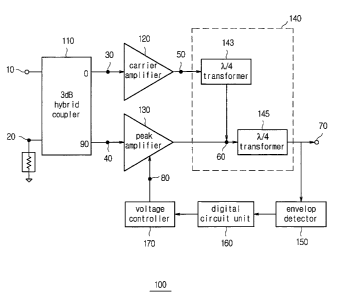
Fig. 1 is a block diagram showing the structure of a power amplifier in a
mobile handset in accordance with one, preferred embodiment of the present
invention.
Fig. 2 shows an equivalent circuit of a 3dB hybrid coupler that can be used in
the preferred embodiment of the present invention.
Fig. 3 is a block diagram of an output matching unit illustrated in Fig. 1.
Fig. 4 shows an equivalent circuit of an output matching unit implemented
with lumped elements.
Fig. 5 is a graph illustrating efficiency characteristics dependent on input
DC-bias voltage applied to a peak amplifier.
Fig. 6 is a graph illustrating non-linearity characteristics dependent on
input
DC-bias voltage applied to the peak amplifier.
Fig. 7 is a graph illustrating efficiency characteristics corresponding to
6
CA 02474975 2004-07-30
WO 03/065599 PCT/KR02/00163
modes of the power amplifier in accordance with the preferred embodiment of
the
present invention.
Fig. 8 is a graph illustrating non-linearity characteristics corresponding to
modes of the power amplifier in accordance with the preferred embodiment of
the
present invention.
Fig. 9 is a graph illustrating gain characteristics corresponding to modes of
the power amplifier in accordance with the present invention.
Fig. 10 is a block diagram showing the structure of a power amplifier in
accordance with a second preferred embodiment of the present invention.
**Description of the codes at important parts of diagrams**
110: 3dB hybrid coupler 120: carrier amplifier
130: peak amplifier 140: output matching unit,
150: envelop detector 160: digital circuit unit
170: voltage controller 180: phase difference compensator
BEST MODE FOR CARRYING OUT THE INVENTION
Hereinafter, a detailed description will be given with reference to the
attached drawings as to an exemplary power amplifier in a mobile handset in
accordance with various embodiments of the present invention.
Fig. 1 illustrates the structure of an exemplary power amplifier in a mobile
handset in accordance with the first preferred embodiment of the present
invention.
The power amplifier 100 illustrated in Fig. 1 comprises a 3dB hybrid coupler
110, a
7
CA 02474975 2004-07-30
WO 03/065599 PCT/KR02/00163
carrier amplifier 120, a peak amplifier 130, an output matching unit 140, an
ervelope
detector 150, a digital circuit unit 160 and a voltage controller 170.
The 3dB hybrid coupler 110 distributes certain input powers to the carrier
amplifier 120 and the peak amplifier 130, minimizes interference between the
carrier
S amplifier 120 and the peak amplifier 130 and transmits signals in such a
manner that
the phase of input power of peak amplifier 130 is 90° (~,/4) delayed
from the phase of
input power of the carrier amplifier 120. Accordingly, the 90° (~,/4)
phase delay
occurring at the output matching unit 140 between the phases of output powers
from
the carrier amplifier 120 and the peak amplifier 130 is compensated and the
phases of
output powers at the output stage are equalized.
As described above, the 3dB hybrid coupler 110's compensation of phase
difference between the phases of output powers from the carrier amplifier 120
and the
peak amplifier 130 obtains the optimum output power by equalizing the phases
of
output powers at the output stage.
Fig. 2 shows an equivalent circuit of the 3dB hybrid coupler 110 in
accordance with the preferred embodiment of the present invention. After
signals
are inputted into input stage 10 of the 3dB hybrid coupler 110, which has the
signal
coupling of about 3dB or more, such signals are transmitted to the carrier
amplifier
output terminal 50 and to the peak amplifier output terminal 60. At this time,
the
signal outputted to the carrier amplifier output terminal 50 and the signal
outputted to
the peak amplifier output terminal 60 have a phase difference of 90°
(~,/4, or quarter-
wave).
As an example, the 3dB hybrid coupler 110 can be implemented with a
transmission line, such as a coupled line coupler, a Lange coupler, a branch
line
8
CA 02474975 2004-07-30
WO 03/065599 PCT/KR02/00163
coupler or other like coupling circuits known in the art. As another example,
the
3dB hybrid coupler 110 may be implemented using a Microwave Monolithic
Integrated Circuit (MMIC) chip. In yet another example, the 3dB hybrid coupler
110 may be implemented with lumped elements 111, 112, 113, 114, 115, 116, 117
and 118, as shown in Fig. 2. In still yet another example, the 3dB hybrid
coupler
110 may be implemented by the Low Temperature Co-fired Ceramic (LTCC)
method.
The carrier amplifier 120 amplifies signals outputted from 3dB hybrid
coupler 110 and outputs the amplified signals. The carrier amplifier 120
includes a
transistor that can be sized smaller than that of a transistor constituting
peak amplifier
130. The ratio of a transistor's size to the other transistor's size, in part,
determines
an output power range over which the maximum efficiency can be maintained. The
higher this ratio, the wider the output power range over which the maximum
efficiency can be maintained.
The peak amplifier 130, which is another amplifier for amplifying signals
outputted from the 3dB hybrid coupler 110 and outputting the amplified
signals, is
not substantially operated while low-level input signals are applied to
carrier
amplifier 120. This is made possible by adjusting the level of input DC-bias
voltage
applied to peak amplifier 130 in such a way that peak amplifier 130 is biased
at class -
B or -C, where little DC current flows. Over the low output power range where
peak amplifier 130 is not substantially operated, the carrier amplifier 120
has output
impedance having a relatively constant and high value. As a result, the
carrier
amplifier 120 can obtain the maximum efficiency at an output power level which
is
lower than the highest output power level that carrier amplifier 120 may
generate.
9
CA 02474975 2004-07-30
WO 03/065599 PCT/KR02/00163
The output matching unit 140 includes a first ~,/4 transformer 143 for
matching impedance of output power applied from carrier amplifier 120 and
transmitting the output power applied from the carrier amplifier 120 to the
output
stage 70; and a second ~,/4 transformer 145 for matching impedance of output
power
applied from the peak amplifier 130 and transmitting the output power applied
from
the peak amplifier 130 to the output stage 70.
Fig. 3 is a block diagram of the output matching unit 140 illustrated in Fig.
1.
By adjusting a and (3 of the first ~,/4 transformer 143 and the second ~,/4
transformer
145, in the output matching unit 140, in the low output power range where the
peak
amplifier 130 is not operated, the carrier amplifier 120 may achieve the
maximum
efficiency at an output power level which is lower than the highest output
power level
that the carrier amplifier 120 may generate.
The first ~,/4 transformer 143 and the second ~,/4 transformer 145 may be
implemented with ~,/4 transmission lines (T-lines), as shown in Fig. 3, or
with lumped
elements 143a, 143b, 143c, 143d, ..., 145a, 145b, 145c, 145d, etc., as shown
in Fig.
4, or with like elements. Alternatively, the first ~,/4 transformer 143 and
the second
~,/4 transformer 145 may be implemented by the LTCC method.
The envelope detector 150 detects the level of output power transmitted from
the output matching unit 140 to output stage 70.
The digital circuit unit 160 is configured to determine whether the output
power level detected by the envelope detector 150 deviates from the low output
power range Q and applies a control signal to the voltage controller 170
according to
the result of the determination.
The voltage controller 170 is configured to control the level of input DC-bias
CA 02474975 2004-07-30
WO 03/065599 PCT/KR02/00163
voltage applied to peak amplifier 130 based on the control signal applied from
the
digital circuit unit 160.
Fig. 5 is a graph illustrating efficiency characteristics as determined by,
for
example, the input DC-bias voltage applied to peak amplifier 130.
As a current starts to flow in peak amplifier 130, the peak amplifier 130
commences its operation. This changes the output impedance of carrier
amplifier
120, thereby optimizing efficiency of power amplifier 100 to a certain
constant level
as indicated by D in Fig. 5. Accordingly, as indicated by curve D in Fig. 5,
the
Power Added Efficiency (PAE) has the maximum value from the point P (when the
peak amplifier 130 starts to operate) to the point when the power amplifier
100
provides the highest output power. Thus, as illustrated, improved efficiency
characteristics are achieved through an exemplary power amplifier, according
to an
embodiment of the present invention, in comparison with the efficiency
characteristic
of a general power amplifier indicated by curve A in Fig. 5. As described
above,
this is made possible by operating the peak amplifier 130 at class -B or -C.
However, illustrated by the graph of Fig. 6 are non-linearity characteristics
as
an input DC-bias voltage is applied to peak amplifier 130. Values of the
overall
non-linearity characteristics (as indicated by curve D in Fig. 6) may be
difficult to
predict and, thus, the non-linear distortion of the power amplifier becomes
undesirable. Accordingly, ACPR criterion R, which may be required by a
specific
system, may not be maintained up to the desired output power level associated
with
point S.
In other words, as illustrated in Fig. 5 and Fig. 6, compared with general
power amplifiers known in the related art, and if the peak amplifier 130 in
the power
11
CA 02474975 2004-07-30
WO 03/065599 PCT/KR02/00163
amplifier 100 is operated at class B or C (that is, if the power amplifier 100
is
operated in a typical Doherty mode), then power amplifier 100 shows improved
efficiency characteristics. However, in terms of linearity, the power
amplifier might
have less predictable values when operating in the high output power range.
Therefore, an exemplary power amplifier in accordance with an embodiment
of the present invention meets high efficiency and linearity requirements in
the low
output power range, such as at point Q, where the ACPR criterion R required by
the
system is satisfied. Criterion R is met by setting the input DC bias voltage
applied
to the peak amplifier 130 in such a way that the peak amplifier 130 can be
operated at
class -B or -C where little DC current flows, and thus that the power
amplifier 100 is
operated in the Doherty mode. On the other hand, in the high output power
range,
the power amplifier achieves excellent linearity by adjusting input DC bias
voltage
applied to the peak amplifier 130 in such a way that the power amplifier 100
is
operated in the operation range (B or A) where the input voltage applied to
the peak
I S amplifier 130 is increased up to point R satisfying the non-linearity
specification of
the power amplifier 100.
Fig. 7 is a graph illustrating efficiency characteristics corresponding to
modes of the power amplifier in accordance with an embodiment of the present
invention. Fig. 8 is a graph illustrating non-linearity characteristics
corresponding to
modes of the power amplifier in accordance with the present invention. Fig. 9
is a
graph illustrating gain characteristics corresponding to modes of the power
amplifier
in accordance with the present invention. In the present invention, the earner
amplifier 120 and the peak amplifier 130 may be operated to have the same
linear
gain characteristics irrespective of the relevant modes. However, the overall
system
12
CA 02474975 2004-07-30
WO 03/065599 PCT/KR02/00163
is not affected even if the carrier amplifier 120 and the peak amplifier 130
are
implemented to be operated with different linear gain characteristics
according to the
relevant modes.
Fig. 10 is a block diagram showing the structure of a power amplifier in a
mobile handset in accordance with second preferred embodiment of the present
invention. The power amplifier according to the second preferred embodiment of
the present invention is substantially the same as the power amplifier 100 of
the first
preferred embodiment, in terms of the structure and operation. Therefore, the
same
reference numerals refer to the same parts in the power amplifiers according
to the
first and the second preferred embodiments. Thus, a detailed description of
the
power amplifier according to the second preferred embodiment will be omitted
herein.
As shown in Fig. 10, another exemplary power amplifier in accordance with
second preferred embodiment comprises a phase difference compensator 180 which
replaces 3dB hybrid coupler 110 of the first preferred embodiment. The phase
difference compensator 180 is connected in between the input stage 10 and the
peak
amplifier 130 to make input signal applied to the peak amplifier 130 and input
signal
applied to the carrier amplifier 120 have phase difference of 90°
(~,/4).
As described above, because input signal applied to the peak amplifier 130
and input signal applied to the carrier amplifier 120 have a phase difference
of 90°
(~,/4) through the operation of the phase difference compensator 180, when the
output
powers from the carrier amplifier 120 and the peak amplifier 130 join in the
output
matching unit 140, there would be no phase difference and thus the optimum
output
power may be obtained.
13
CA 02474975 2004-07-30
WO 03/065599 PCT/KR02/00163
If a phase difference compensator 180 is used instead of the 3dB hybrid
coupler 110, the phase difference compensator 180 may be implemented with one
simple transmission line. Alternatively, the phase difference compensator 180
may
be implemented with lumped elements because the simple transmission line may
be
approximated to inductance values. In this manner, the power amplifier rnay be
implemented without a complex 3dB hybrid coupler 110 or a lauge-size
transmission
line outside of the amplifier. Furthermore, because the phase difference
compensator 180 may be integrated within a single chip, the overall size of
the power
amplifier 100 may be reduced and the price of the power amplifier 100 may also
be
reduced.
Hereinafter, a detailed description will be given as to the operation of the
power amplifier in a mobile handset implemented according to the present
invention.
The envelope detector 150 detects the level of output power transmitted to
the output stage 70 and supplies the detection result to the digital circuit
unit 160.
Then, the digital circuit unit 160 determines whether the output power level
detected
by the envelope detector 150 deviates from the low output power range Q and
applies
a control signal to the voltage controller 170 in accordance with the result
of such
determination. If the level of output power transmitted to the output stage 70
is
within the low output power range Q (mode 0), the voltage controller 170
controls
input DC-bias voltage applied to the peak amplifier 130 in such a manner that
the
power amplifier 100 is operated in the Doherty mode (i.e., so that the peak
amplifier
130 is operated at class -B or -C). In contrast, if the level of output power
transmitted to the output stage 70 deviates from the low output power range Q,
(namely, in the high output power range) (mode 1), the voltage controller 170
14
CA 02474975 2004-07-30
WO 03/065599 PCT/KR02/00163
controls input DC-bias voltage applied to the peak amplifier 130 in such a
manner
that the input DC-bias voltage applied to the peak amplifier 130 is increased
so that
the ACPR is improved up to point R where the non-linearity specification of
the
power amplifier 100 is satisfied.
Although several embodiments of the present invention have been disclosed
for illustrative purposes, those skilled in the art will appreciate that
various
modifications, additions and substitutions are possible, without departing
from the
scope and spirit of the invention as disclosed in the accompanying claims.
INDUSTRIAL APPLICABILITY
As described above, the present invention provides a power amplifier in a
mobile handset that improves efficiency and linearity, by controlling an input
DC-
bias voltage applied to a peak amplifier according to the relevant output
power levels.
Specifically, in the low output power mode, input DC-bias voltage to the peak
amplifier is controlled so that the power amplifier of the present invention
is operated
in the Doherty mode and, in the high output power mode, input DC-bias voltage
to
the peak amplifier is controlled to be increased so as to satisfy the non-
linearity
specification of the power amplifier.
Further, according to the present invention, the power amplifier can be
implemented through a simple process, and the size and the price of the power
amplifier may be reduced because only input DC-bias voltage applied to the
peak
amplifier is controlled.