Note: Descriptions are shown in the official language in which they were submitted.
CA 02475294 2004-08-04
WO 03/067516 PCT/US03/01084
Inventor: Scribner PATENT APPLICATION
Serial No. PCT No.
MICROELECTRONIC STIMULATOR ARRAY
BACKGROUND OF THE INVENTION
Field of the Invention
This invention deals generally with neural prosthesis, specifically the
concept of
achieving a retinal prosthesis for blind patients through the creation of an
electrical interface
between a high-density electrode array and the curved surface of the retina.
Description of the Related Prior Art
There is a great deal of recent interest in the area of neural prosthesis,
specifically the
concept of achieving a retinal prosthesis for blind patients has been
hypothesized by a number
of researchers and is an active area of medical research. In a normal eye, in
a basic concept
10, Figures 1a and 1b shows a ray trace of two photons 12 focused on a retina
21. Note that
the incoming photons 12 pass through several layers of transparent retinal
cells 16 and 18
before being absorbed by the photoreceptors 22. In a damaged eye, a retinal
prosthesis
device 24, as shown in Figures 1c and ld, is positioned against the retina 21.
In this case, the
photons 12 are absorbed by a microelectronic stimulating array or device 26
that is
hybridized to a glass piece 28 containing an embedded array of microwires. The
glass has a
curved surface that conforms to the inner radius of the retina 21. The
microelectronic
imaging device 26 is made of thin silicon containing very large scale
integrated (VSLI)
circuitry and photon detectors that convert the incident photons 12 to an
electronic charge.
CA 02475294 2004-08-04
WO 03/067516 PCT/US03/01084
Inventor: Scribner PATENT APPLICATION
Serial No. PCT No.
The charge is then converted to a proportional amount of electronic current
which is input to
the nearby retinal cell layer 18. The cells fire and a signal is sent to the
optic nerve 28.
A typical retinal prosthesis device combines two technologies: first,
nanochannel
glass (NGC) electrode arrays and secondly a two-dimensional (2-D) multiplexer
array. NGC
technology employs fiber optic fabrication techniques to produce thin wafers
of glass with
very small channels perpendicular to the plane of the wafer. Typical NGC
wafers that will
be required for retinal prosthesis devices are several millimeters in diameter
and can contain
millions of channels with channel diameters on the order of one micron. The
channels are
filled with a good electrical conductor and one surface of the glass is ground
to a spherical
shape consistent with the radius of curvature of the inside of the retina. The
electrical
conductors on the curved surface should protrude slightly to form efficient
electrodes.
The 2-D multiplexer array is similar to infrared focal plane array (IRFPA)
multiplexers that are microelectronic devices fabricated at silicon foundries.
An IRFPA
multiplexer is a 2-D array that reads out the infrared (IR) image captured by
a complimentary
detector array that converts photons into electrical charge. The charge is
integrated and stored
in each unit cell for a few milliseconds. The full image is then multiplexed
off the array at
frame rates compatible with commercial video. For a retinal prosthesis test
device that
obtains its input image from an external camera, the process is essentially
reversed and the
device acts as a de-multiplexer. That is, the prosthesis devices will perform
de-multiplexing
operations, but will be referred to here simply as a multiplexer.
The basic concept is straightforward: visual images can be produced in the
brain by
2
CA 02475294 2004-08-04
WO 03/067516 PCT/US03/01084
Inventor: Scribner PATENT APPLICATION
Serial No. PCT No.
electrical stimulation of retinal cells. Two-dimensional arrays of retinal
cells, such as
ganglion or bipolar cells, can be stimulated using two-dimensional arrays of
electrical
impulses with the spatial form of an image. The axons of the ganglion cells
then transmit the
image through the optic nerve and on to the visual cortex. This is in lieu of
the normal photo-
transduction process that occurs in a healthy retina. In approximately 90
percent of blind
patients, the photoreceptors are diseased, but the other retinal layers are
still responsive to
electrical stimulation.
Experimental test procedures, such as shown in Figure 2, use standard retinal
surgical
techniques performed in an operating room environment by an ophtalmologist. It
is necessary
that the patient be administered local anesthesia rather than general
anesthesia so that visual
perceptions can be orally recorded during the procedure.
There are a number of technical issues to be addressed in designing and
fabricating a
retinal prosthesis device, particularly if the device is to generate a high
resolution image.
First, there is the issue of creating an electrical interface between the high-
density electrode
array and the curved surface of the retina. The electrode array must have a
spherical,
convexed shape in order to conform to the spherical concaved surface of the
retina. The
electrode array must be bio-compatible and safe for permanent implantation.
Second, the
electrical stimulation pulse shapes and repetition rates, while generally well
known, may need
to be optimized for each individual recipient of a prosthesis device. The
pulse amplitude is of
course modulated within the retina to be proportional to the pixel value.
Third, direct
electrical stimulation of the ganglion cells precludes certain image
processing functions that
3
CA 02475294 2004-08-04
WO 03/067516 PCT/US03/01084
Inventor: Scribner PATENT APPLICATION
Serial No. PCT No.
normally would have occurred in earlier layers of the retina. Therefore,
computationally
based image preprocessing operations may need to be performed on the image
before
stimulation of the retina. Fourth, supplying power to a permanent implant will
need to be
engineered in a manner such that there are no wires or cables through the eye
wall. Fifth,
because a normal retina processes image information created by the
photoreceptors in a
simultaneous manner, it is assumed that a prosthesis device should similarly
excite retinal
cells in a simultaneous manner, as opposed to sequential raster scan that
might cause
synchronicity problems downstream in the lateral geniculate nucleus (LGN) or
visual cortex.
SUMMARY OF THE INVENTION
An object of this invention is to provide a device for achieving a retinal
prosthesis for
blind patients.
Another object of this invention is to provide a retinal prosthesis test
device for
providing visual images to the brain during acute human experiments to achieve
electrical
stimulation of the retina tissue.
Another object of this invention is to provide a device for implant into the
human eye
that will allow electrical stimulation of the retinal or any neural tissue so
as to provide visual
images to the brain.
These and other objects are accomplished by the retinal prosthesis test device
and
retinal implant device comprising two basic technologies -- nanochannel glass
(NGC)
electrode arrays and infrared focal plane array (IRFPA) multiplexers. In the
retinal prosthesis
4
CA 02475294 2004-08-04
WO 03/067516 PCT/US03/01084
Inventor: Scribner PATENT APPLICATION
Serial No. PCT No.
test device, the device is positioned against the retina using standard
retinal surgical
techniques in an operating room environment. The device is comprised of a thin
wafer of
glass (NGC) with very small channels perpendicular to the plane of the wafer.
The channels
are filled with a good electrical conductor forming microwires with one
surface of the glass
being ground to a spherical shape consistent with the radius of curvature of
the inside of the
retina. Electrical conductors protrude slightly from the NGC on the curved
surface to form
electrodes. The NGC is hybridized to a silicon IRFPA multiplexer using indium
bump
bonds. An image is serially input into the multiplexer via a very narrow,
flexible micro-
cable. The multiplexer is mounted on a ceramic carrier such that
interconnecting bond pads
on each are in close proximity to one another. A video image is read into each
of the unit
cells on the multiplexer in pixel-by-pixel manner. Discrete samples of the
analog video are
input and stored as electrical charge on a MOS capacitor. After all unit cells
have been loaded
with the pixel values for the current frame, a biphasic pulse is sent through
each unit cell and
into the corresponding area of the retina. The biphase pulse is modulated in
proportion to the
pixel value stored therein. Because the biphasic pulse flows in parallel from
a global external
connection, the adj acent retinal neurons are all stimulated simultaneously,
analogous to image
photons stimulating photoreceptors in a normal retina.
A permanent retinal implant device uses an NGC array hybridized to a silicon
chip in
an identical manner to the retinal prosthesis test device, however, the image
is no longer
multiplexed onto the chip through a wire from an external camera, but instead,
the image is
simultaneously generated within each cell through a photon-to-electron
conversion using a
5
CA 02475294 2004-08-04
WO 03/067516 PCT/US03/01084
Inventor: Scribner PATENT APPLICATION
Serial No. PCT No.
silicon photodiode. The photons propagate directly into the backside of the
device.
Electrical power and any control signals are transmitted through an
inductively driven coil or
antenna on the chip. The device collects the charge in storage capacitors via
the photon-to-
electron conversion process, stimulates the neural tissue with biphasic pulses
in proportion to
the stored charges, and resets the storage capacitors to repeat the process.
BRIEF DESCRIPTION OF THE DRAWINGS
Figure 1a shows a general diagram of a ray trace of photons incident on a
retina
without a prosthesis device (a normal eye).
Figure 1b shows an interior view of a ray trace of photons incident on a
retina
without a prosthesis device (a normal eye).
Figure 1c shows a general diagram of a ray trace of photons incident on a
retina with
a prosthesis device ( prosthesis device positioned against the retina).
Figure 1d shows an interior view of a ray trace of photons incident on a
retina with a
prosthesis device (prosthesis device positioned against the retina).
Figure 2 shows a retinal prosthesis test device positioned against a retina.
Figure 3a shows a side-view of a fully packaged retinal prosthesis test
device.
Figure 3b shows an enlarged view of a nano-channel glass (NCG) electrode
array.
Figure 4 shows a conceptual layout (floor plan) of a silicon chip for the
retinal test
prosthesis.
Figure 5 shows a conceptual design of a unit cell for the retinal prosthesis
test device
6
CA 02475294 2004-08-04
WO 03/067516 PCT/US03/01084
Inventor: Scribner PATENT APPLICATION
Serial No. PCT No.
showing the external inputs from off-chip.
Figure 6 shows a block diagram of ancillary electronics for the retinal
prosthesis test
device.
Figure 7 shows a side-view of a permanent implant device.
Figure 8 shows a conceptual design of a unit cell for a permanent implant
device.
Figure 9 shows a conceptual layout (floor plan) of a silicon chip for a
permanent
implant device.
DESCRIPTION OF THE PREFERRED EMBODIMENT
In the preferred embodiment of a retinal prosthesis test device utilizing a
microelectronic stimulator array 30, as shown in Figure 3a, the nanochannel
glass (NGC)
electrode arrays 32 is hybridized to silicon multiplexer 34 using indium bump
bonds, a
technique from infrared (IR) focal plane array (1RFPA) multiplexers. An image
is serially
input onto the multiplexer 34 via a very narrow, flexible micro-cable 36. The
micro-cable 36
is approximately six inches in length and is custom made using gold leads
patterned on
polyimide strips. A ceramic carrier 38 with gold-filled via holes 42 provides
a mechanically
convenient means of routing interconnects from the top-side 44 of the ceramic
carrier to the
back-side 46. By designing the ceramic carrier such that the top-side contacts
to the via-holes
44 are in close proximity to bond pads 48 on the silicon multiplexer 34, the
interconnection
may be made with conventional tab-bonds 52 (thin gold ribbons fused to
interconnects with
mechanical pressure as is common practice in the microelectronics industry and
is well
7
CA 02475294 2004-08-04
WO 03/067516 PCT/US03/01084
Inventor: Scribner PATENT APPLICATION
Serial No. PCT No.
known to those skilled in the art. This keeps all of the interconnects 52 from
protruding
above the spherical curved envelop defined by the polished NCG 32 and
therefore prevents
damage to the tab bond interconnects 52 or to a patients retina 54. A critical
issue for any
neural prosthesis device is biocompatibility and safety. Because the duration
of any tests with
the retinal prosthesis test device 30 are very short (less than an hour),
biocompatibility issues
are primarily reduced to acute effects of the testing and need not address the
more difficult
chronic issues that arise with permanent implants. Note that the surface of
the packaging
shown in Figure 3a consists only of glass 32 , platinum (Pt) electrodes 56 ,
and silicon
encapsulation 5~. However, as with any medical instrumentation, a major safety
issue is
electrical shock hazard. Note that the purpose of the device is to provide
minimal electrical
stimulation of retinal tissue using very low voltages and the smallest current
possible, i.e.,
preferably about one volt and 1 ALA per unit cell for about 1 millisecond
(every frame at a
frame rate of 60 Hz). To protect a patient from any electrical shock, the
patient is isolate from
high voltages using optocouplers (not shown) which are powered by low voltage
electrical
batteries (not shown), a technique well known to those skilled in the art.
Specific requirements for the NCG 32 are that the channels 56 making up the
NCG
32, as shown in Figure 3b, be small enough so that many microwires can be
connected to
each unit cell of the multiplexes array. This is for redundancy and to help
simplify the
hybridization alignment. If the NCG wires were to approach the size of the
unit cell, then a
one-to-one alignment and hybridization would be required. This would be very
problematic,
because of irregularities in the NCG periodicity and the possibility of
shorting nearest
8
CA 02475294 2004-08-04
WO 03/067516 PCT/US03/01084
Inventor: Scribner PATENT APPLICATION
Serial No. PCT No.
neighbor cells (not shown). On the other hand, very narrow channels 56 imply
very high
length-to-width aspect ratios of the channels 56 in the NCG 32. This makes it
difficult to
fabricate large area NCG 32 samples with the proper thickness. It is expected
that a
reasonable design size for the channels 56 should be on the order of a micron.
The NCG channels 56 must be filled with a high conductivity material 62, such
as
platinum, to create microwires. Fabrication of the microwires can be performed
using
electrodeposition or infusion of molten metal under pressure, techniques that
are well known
to those skilled in the art. After the channels 56 have been filled with
conductive material
and the continuity of the microwires has been confirmed, one side of the glass
32 must be
polished to create a spherical surface 64. This is accomplished by carefully
grinding and
polishing of the glass/metal composite. The radius of curvature is nominally
half an inch in
order to provide a conformal fit against the inside of the retina 54. This is
critically important
as it allows positioning of the high-density electrodes in the NCG 32 against
the retinal 54
tissue. The polishing process will create slightly recessed microwires with
respect to the
curved NCG 32 surface. This is because the metal is softer than the glass.
Therefore further
processing may be necessary to create electrodes that protrude slightly above
the curved
surface 64 of the NCG 32. In preparation for hybridizing the NCG 32 to the
multiplexes 34,
or the microwires may be hybridized directly to the indium bumps 66 on the
multiplexes 34
or the glass is etched so the microwires protrude slightly from the NCG 32.
This is similar to
the manner used to form the protruding electrodes on the curved side 64 of the
NCG 32.
A conceptual layout of the multiplexes 34 is shown in Figure 4. The silicon
9
CA 02475294 2004-08-04
WO 03/067516 PCT/US03/01084
Inventor: Scribner PATENT APPLICATION
Serial No. PCT No.
multiplexes 34 performs several operations in a sequential order. During the
first step, an
image is read onto the multiplexes 34, pixel-by-pixel to each unit cell 72.
The row shift
register 74 and column shift register76 control the routing into each unit
cell 72. The discrete
samples of analog video are input and stored as charge on MOS capacitor. This
operation
occurs every 60"' of a second in a manner compatible with a RS-170 television
format
allowing the use of the test prosthesis 30 with standard video equipment. A
multiplexes 34
that has a read-on and read-off capability has several input signals including
a pixel clock,
start-of-frame clock, bias voltage, ground, and analog input (RS-170). A
digital electronics
block 78 is of major importance because it generates switching pulses that
routes image data
into the unit cells 72 by controlling the row shift register 74 and the column
shift register 76..
Without the on-chip digital electronics 78, there might be a dozen or more
clocks that would
need to be input to the device. That would make the cable 27 from external
drive electronics
through the eye wall 29 (as shown in Figure 2) much larger and more
cumbersome. The
use of IRFPA multiplexes technology greatly simplifies cable 27 problems
through the eye
wall 29.
20 Referring again to Figure 4, after all the unit cells 72 have been loaded
with the pixel
values for the current frame, the next step is to send a biphasic pulse to
that unit cell 72
which in turn is modulated in proportion to the pixel value stored in each
unit cell 72.
Because the biphasic pulse flows in parallel from a global external
connection, the adjacent
retinal neurons are all stimulated simultaneously. This is an important
feature of the design
25 because it is synchronistic action analogous to imaged photons stimulating
photoreceptors in
CA 02475294 2004-08-04
WO 03/067516 PCT/US03/01084
Inventor: Scribner PATENT APPLICATION
Serial No. PCT No.
a normal retina. Finally, the electrodes are all connected to ground to
prevent any possible
charge build up at the electrode-neuron interface.
There are several important consideration in designing a device that performs
all these
operations successfully. First the multiplexes 32 operation should be designed
with many of
the requirements that exist for an IRFPA, for example, good uniformity, low
noise, and high
dynamic range. Of course, the retinal prosthesis test device 30 moves image
data in the
opposite direction than an IRFPA multiplexes, that is, image data moves onto
the device
rather than off the device, but otherwise the specifications are analogous.
Figure 5 shows a
generic design for a unit cell 72. Note that the unit cell 72 stores the pixel
value and then
uses it to modulate the biphasic pulse 82 that is input to the retinal tissue
54 through the NCG
32. Note that the biphasic pulse 82 and the image data 84 are both generated
off-chip. This
allows for greater flexibility during human testing as any image sequence can
be input and
combined with any shape of biphasic pulse 82. The switch 86 at the bottom of
Figure 5
provides the capability to connect the retinal tissue 54 to ground 88 to avoid
any possibility of
charge build-up.
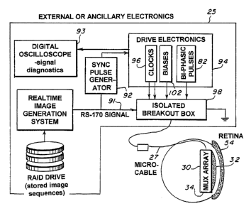
Referring to Figure 6, the operation of the retinal prosthesis test device 30
during
acute experiments is controlled and powered by external ancillary electronics
25. The input
signal is an image sequence at data rates fast enough to achieve 60 frames per
second. The
multiplexes 34 is designed to sample the multiplexed input signal in a manner
compatible
with the RS-170 format. This allows the retinal prosthesis test device 30 to
be interfaced
directly with any standard video camera. This includes the use of a computer
which stores
11
CA 02475294 2004-08-04
WO 03/067516 PCT/US03/01084
Inventor: Scribner PATENT APPLICATION
Serial No. PCT No.
digital imagery and can display sequential fields at a 60 Hz rate (RS-170
interlaces two fields
per frame at a rate of 30 frames per second). The actual control of the
microelectronic
multiplexes 34 is done with precisely timed pulses generated by a set of
signal clocking
boards 96 in a manner similar to that used in typical IRFPA's. The sync pulse
generator 92 is
used to synchronize the RS-170 signal 91 with the clocking pulses 96.
Basically, the sync
pulse generator 92 detects the beginning of each RS-170 field and then sends a
corresponding
pulse to the drive electronics 94 that triggers the clocking signals 96
required to control each
field of the image data input to the multiplexes 34, synchronizaton of the
pulses can be
monitored with an oscilloscope 93. The isolated breakout box 98 electrically
isolates the
human subject from high voltage power supplies. The box 98 contains opto-
couplers that
isolate the clock 96 and biphasic pulse signals 82 and low voltage batteries
supplying bias
potentials 102. .
The biphasic pulses 82 used to stimulate the retinal tissue 54 may be
programmable
such that any pulse shapes can be tested. This has several important
implications for the
development process. First, because the input impedance to the retinal tissue
54 has both a
resistive and capacitive reactance associated with it, a square wave voltage
pulse will not
produce the desired square wave current pulse. Neurobiologists tend to favor
square wave
current pulses to achieve efficient neural stimulation. With knowledge of the
output
impedance at the electrode-retina interface, a voltage shape can be computed
that will provide
a square wave current pulse, thus providing efficient stimulation. Second,
there is evidence
that various layers of the retina 54 can be stimulated with different shaped
pulses - probably
12
\
CA 02475294 2004-08-04
WO 03/067516 PCT/US03/01084
Inventor: Scribner PATENT APPLICATION
Serial No. PCT No.
because of their differing frequency responses. Specifically, it is expected
that either the
ganglion or bipolar cells can be selectively stimulated. Stimulating the
bipolar cells instead
of the ganglion cells has the advantage of reaching more deeply into the
retina 54, allowing a
more natural form of stimulation.
Direct electrical stimulation of the ganglion cells precludes certain
processing
functions that normally would have occurred in the earlier layers of the
retina 54. Therefore,
it may be necessary to perform certain functions on the incoming imagery
before stimulation
to compensate for the missing processing. Unfortunately, a detailed model of
human retinal
functions has never been confirmed. Nevertheless, it has been shown that many
intracellular
recordings from the retinas of rabbits are very similar in mammailian vertebra
species in
general.
In another preferred embodiment, a permanent implant device 40, as shown in
Figure
7, that is fully self-contained and responds to incident photons naturally
imaged through the
lens of the eye, similar to that shown in Figures 1c and ld, is taught. The
device 40 is
surgically implanted in a patients eye and has with no external connections
passing through
the eye wall. The basic design of this device 40 is based extensively on the
retinal prosthesis
test device 30 taught above. Specifically, the permanent implant device 40
would use a NCG
array 102 hybridized to a silicon chip 104 in an identical manner to the
retinal prosthesis test
device 30. However, the unit cell 106 circuitry is redesigned because the
image is no longer
being multiplexed onto the chip through a cable from an external camera, but
instead, the
image is simultaneously generated within each unit cell 106 through a photon-
to-electron
13
CA 02475294 2004-08-04
WO 03/067516 PCT/US03/01084
Inventor: Scribner PATENT APPLICATION
Serial No. PCT No.
conversion using a silicon photodiode 108, as shown conceptually in Figure 8.
The photons
112 propagate directly into each unit cell 106 because the silicon chip 104 is
used in a back-
illuminated configuration -- essentially the photons 112 enter through the
backside of the
silicon chip 104.
Packaging the device 40, obviously, differs from that of the retinal
prosthesis test
device 30. Packaging the permanent implant device 40 requires that the photons
112 be
allowed to pass through the backside of the device 40. This is a simple matter
of eliminating
the ceramic carrier taught in the retina prosthesis test device 30. Thinning
the silicon chip
104 is necessary because of the need for good quantum efficiency. The
packaging scheme for
the permanent implant device 40 is shown in Figure 7. Note that the silicon
chip 104 can be
thinned to a few tens of microns so that the overall mass of the object is
primarily that of the
NCG array 102 making it more amenable for surgical attachment to the retina
114.
It will be noted that there is no need for any multiplexing functions in the
permanent
implant device 40, therefore the design of the chip 104 is much simpler. Also
there are no
ancillary electronics, however, the silicon chip 104 significantly differs
from that previously
set forth, as shown in Figure 9. Although there are no multiplexing
requirements, there are
two new requirements, Specifically, these are external power and command
signals necessary
to adjust the operation of the device 40. Transmitting power and signals onto
the device 40
are implemented with an inductively driven coil or antenna 116. The major on-
chip electronic
adjustments needed are control of bias supplies 118 and biphasic pulse
generator 122 plus the
14
CA 02475294 2004-08-04
WO 03/067516 PCT/US03/01084
Inventor: Scribner PATENT APPLICATION
Serial No. PCT No.
standard digital electronics 124 that supply timing for the simultaneous
operation of the unit
cell 106 sequences. Again the operation of the device 40 is to collect charge
in the storage
capacitors of the unit cells. The on-chip power receiver 126 provides
conditioned power to
operate all the on-chip electronics. The frame rate would be nominally 60
frames per second,
but because there is no longer a need to be compatible with the RS-170 format,
the frame rate
could be adjusted to anything desired.
Pacleaging of the permanent implant device 40 is very demanding. Along with
issues
of biocompatibility is the question of device lifetime. Permanent implants
might need to
operate for several decades. Similar requirements exist for other electronic
implants such as
cardiac pacemakers and cochlear prosthetics. The encapsulation of the
permanent implant
device 40 is easier in one respect than that of the retinal prosthesis test
device 30 there are no
connecting cables to the device 40. In the case of the latter device 30,
encapsulation was not
a critical issue because the duration of the experiments are typically less
than one hour.
Cables connected to any neural prosthesis are subject to mechanical forces
that over time can
damage seals and ultimately cause failures. Because the permanent implant
device 40 is
completely wireless (no cable connections), simple encapsulation should be
achievable with
high integrity.
The specific teachings of this approach to neural implants is a new intra
ocular device,
and has several extremely important advantages over any device taught by the
prior art. First,
the use of the NCG enables the creation of a curved surface allowing the
positioning of the
electrodes in extremely close proximity to the retinal cells over a large
area. NCG also allows
CA 02475294 2004-08-04
WO 03/067516 PCT/US03/01084
Inventor: Scribner ~ PATENT APPLICATION
Serial No. PCT No.
the creation of very small electrodes (on the order of a micron) with very
high densities
(thousands of electrodes per square millimeter). Regarding the multiplexes for
the retinal
prosthesis test device 30, as well as the unit cell size for the permanent
implant device 40, the
unit cell size can be made as small as practical based on the latest
microelectronic design
rules.
The multiplexes technology taught in the retinal prosthesis test device 30
uses only a
small number of electrical leads through the eye wall while allowing a high
data rate to the
retina. In essence, this allows the input of image sequences to the retina, at
high resolution
and rapid frame rates. The electrical leads may be fabricated on a small and
flexible
microcable. This is critical to performing human experiments and testing. This
is in
comparison to directly coupling all stimulating electrodes to individual
leads. For example, a
simple 8 x 8 test array when directly coupled to input electronics outside the
eye would
require 64 input leads. The cabling and accompanying connectors for such a
device becomes
very cumbersome.
The devices taught here 30 and 40 basically solves the technical problems of
an earlier
concept envisioned by the research group at the Wilmer Ophthalmological
Institute working
with North Carolina State University (NCSU). An approach similar to NCSU is
also under
study by an MIT/Harvard team. Other efforts are proceeding in the United
States, Germany
and Japan that build on the basic idea of stimulating retinal cells with a
small number of
electrodes on a microelectronic chip. However, none of these approaches
addresses the
difficult issue of high-density electrodes in close proximity to the retina
for achieving very
16
CA 02475294 2004-08-04
WO 03/067516 PCT/US03/01084
Inventor: Scribner PATENT APPLICATION
Serial No. PCT No.
high-resolution imagery.
A second approach is to stimulate the retina with a microelectronic chip from
behind
the retina, either replacing the diseased photoreceptors or positioning the
chip just behind
them.
A third approach is to skip the retina altogether and stimulate the visual
center of the brain.
In this approach, an array, with penetrating microelectrodes is positioned
against a visual
cortex. This involves invasive brain surgery through the cranium. From a
surgical point of
view, the intra ocular approach is the least invasive.
Although this invention has been described in relation to an exemplary
embodiment
thereof, it will be understood by those skilled in the art that still other
variations and
modifications can be affected in the preferred embodiment without detracting
from the scope
and spirit of the invention as described in the claims.
17