Note: Descriptions are shown in the official language in which they were submitted.
CA 02476174 2004-08-12
Low-coherence interferometric apparatus
for light-optical scanning of an object
1o The present invention refers to a low-coherence
interferometric apparatus for light-optical scanning of
an object by detecting the position of light-remitting
sites which are located, at variable distances from the
apparatus, along a scan path which extends in a scan
direction (i.e. in the direction of the detection light
beam; "z-direction"). Hereafter this is referred to as
Low Coherence Distance Scan (LCDS).
Such apparatuses, and the corresponding methods are
2o utilized for examining a variety of objects. They allow
to determine, with a highest level of precision, the
distance to one or a plurality of reflecting sites of an
object or to provide a tomographical picture. Significant
areas of use are the automatic measurement of object
surfaces and analysis of the optical scattering behavior
inside an object. The latter is especially significant in
the medical field (tissue diagnostics).
In some applications it is sufficient to scan the object
onedimensionally, i.e. only along a scan path which
extends in the direction of the beam. Most cases of use,
however, require to obtain, by means of an additional
lateral scan, information about reflecting structures in
a scan plane or (three-dimensionally) in a volume
segment. This requires a two- or three-dimensional scan,
which, in the simplest case, may be achieved by one- or
CA 02476174 2004-08-12
2
two-dimensional lateral shifting of the interferometer.
Such methods allow generation of a multidimensional
tomographical picture and are commonly called OCT
(Optical Coherence Tomography).
It is common to all LCDS methods that light of a low-
coherent (spectrally broadband emitting) light source is
split into two light paths, i.e. a measurement light
path, which penetrates into the test specimen, and a
l0 reference light path. Before striking a detector, both
partial 'light paths are combined in such a manner that
interference occurs. To this end the apparatus contains
an interferometer device, which, in addition to the low-
coherent light source, usually contains a beam divider, a
reference reflector and the detector. The light paths
between these elements form interferometer arms. The
light from the light source passes through a light source
arm to the beam divider, where it is split. A first
fraction of light is irradiated, as measurement light,
onto the object in the scan direction, whilst a second
portion of light, as reference light, reaches the
reference reflector via a reflector arm. Both light
fractions are reflected (the measurement light at light
reflecting sites in the examined object, the reference
light at the reference reflector) and travel back along
the same light path (object arm, reference arm) to the
beam divider. Here the light fractions are recombined and
further transported as detection light via a detector arm
to the detector.
During scanning, the longitudinal scan position is being
varied in a,fast sequence. Normally, this is achieved by
changing the relationship of the path lengths of the
reference light path and the measurement light path.
Thereby the position along the scan path is varied, for
CA 02476174 2004-08-12
3
which the conditions for interference of the measurement
light and the reference light are met (namely that the
optical path lengths of both light paths differ by no
more than the coherence length of the light source). At
each point of time the present scan position is the
position on the scan path for which the optical length of
the measurement light path is the same as the optical
length of the reference light path (from the beam
division to the beam junction; "Coherence condition").
to Normally, the reference mirror is displaced in the
direction of the reference beam, thereby reducing or
increasing the length of the reference light path.
Further details about a plurality of known LCDS devices
are described in corresponding literature sources,
including the following publications:
1) WO 95/33971
2) J. M Schmitt "Compact in-line interferometer for low
coherence reflectometry", Optic Letters 1995, 419
through 421.
3) WO 97/27468.
The present invention refers especially to applications
in which an extremely fast longitudinal scan is desired.
An important example is the continuous examination of
multilayer foils (multi-foils) for production
surveillance or quality control. The foil passes with
high speed along a measurement head, and continuous
control has to be applied to determine whether a certain
desired foil thickness (for example 100 Vim) is maintained
within predetermined limits. Such cases of utilization
require a very high scan speed. Assuming, for example, a
surface spot diameter, to which the examination refers,
of 8 ~m and a travel speed of 10 m/sec, measurement data
CA 02476174 2004-08-12
4
would have to be recorded approximately every 0,8 sec.
This corresponds to a minimum scan rate of 1,25 MHz. At
256 spots per longitudinal scan, this results in a
repetition rate of 4,9 kHz. Such high repetition rates
cannot be achieved by a mirror displacement.
Several proposals have been made to achieve a higher
repetition rate with LCDS devices.
l0 In the publication
4) K.F Wong et al: "400-Hz mechanical scanning optical
delay line", Optics Letters 1993, 558-560,
an optical retarding section is described, which may be
integrated into the reference arm of an interferometer.
The variation of the optical path length is achieved by a
combination of an angular dispersion grating and a mirror
which is pivotable within a very restricted angular
range.
A similar device is also described in
5) US Patent 6,111,645 and
6) G.J. Tearney et a1: High-speed phase- and group-delay
scanning with a grating-based phase control delay
line", Optics Letters 1997, 1811-1813,
as part of a LCD device which is reported to be suitable
for extremely fast scanning. In these publications, the
basic principle used in citation 4) is generalized in the
sense that a dispersion grating should be utilized in
connection with a spectral phase shifter. Also non-
mechanical possibilities for the realization of a
spectral phase shifter, especially an acousto-optical
modulator (AOM), are described.
CA 02476174 2004-08-12
A disadvantage of these proposals is the double passage
of light through the retarding unit composed of the
angular spectral grating and optical phase shifter which
requires a very difficult alignment, since a precise
5 reentrance into a single-mode light conducting fiber is
required. Additionally, a high loss of intensity is
caused by this light path.
Additional efforts for solutions proposed by the prior
to art are discussed in the initial sections of citations 5)
and 6 )
A modification of the optical path length may be
achieved by piezoelectric fiber stretching. This,
however, requires a relatively large-sized unit and
does not allow a sufficiently high repetition rate. In
addition, the energy consumption is high.
- The longitudinally moveable mirror in the reference
channel may be replaced by a pivoting glass cube (see
also US Patent 6,144,456). This causes, however, a
non-linear change of the optical path length and a
dispersion which depends on the optical path length.
Again, the achievable repetition rates do not satisfy
high requirements.
Based on this situation the technical problem addressed
by the present invention is to provide an interferometric
apparatus which allows, with tolerable expenditure, an
extremely high repetition rate of longitudinal scanning.
This problem is solved by a low-coherence interferometric
apparatus for light-optical scanning of an object, by
detecting the position of light-remitting sites which are
located along a scan path running in a scan direction,
with a low-coherence interferometer comprising a low-
coherent light source, a reference reflector and a
CA 02476174 2004-08-12
detector, wherein light emitted from the light source is
split by a beam divider into two optical paths and a
first fraction of the light is irradiated as measurement
light onto the object and reflected at a light-remitting
site located at a variable scan position on the scan
path, and a second fraction of the light is irradiated as
reference light onto the reference reflector where it is
reflected, the adjustable scan position is varied along
the scan path to perform a scan, and the measurement
to light and the reference light are combined at a beam
junction~in such a manner that the resulting detection
light, upon striking the detector, generates an
interference signal which contains information about the
reflection intensity of the measurement light relative to
the respective scan position, characterized in that a
variable wavelength selection device is positioned in the
light path of the detection light between the beam
junction and the detector, by which a wavelength-
dependent selection of the detection light is performed
in such a manner that the detector selectively receives
preferably light with wavelengths which correspond to a
predetermined sequence of wavenumbers k, and different
sequences of wavenumbers k can be set for varying the
scan position along the scan path.
Contrary to the above explained earlier efforts to
achieve extremely fast longitudinal scans, the scanning
unit for setting the scan position is integrated in the
light path of the detection light downstream from the
joining of the reference light and the measurement light.
According to the invention the variation of the
longitudinal scan position is not based on a change of
the relationship of the length of measurement- and
reference light paths, but on a selection of a sequence
of wavelengths of the interfering detection light. This
CA 02476174 2004-08-12
7
selection is varied by means of the wavelength selecting
device in such a manner that the sequence of wavenumbers
("k-profile of the wavelength selecting device)
corresponding to the selected wavelengths coincides with
that k-profile of the interferometer which corresponds to
the respective scan position. This will hereafter be
explained in detail, based on the figures.
The physical phenomenon utilized in the invention has
to been known for a long time as so-called "Muller stripes".
Occasionally, it was also used in the context of
interferometric methods. BE 4309056 describes the
possibility to determine the distance of light scattering
sites, i.e. their intensity distribution in the direction
of the detection beam, by spectrally decomposing the
light by means of a spectral device, the spectrum being
detected with a location-sensitive light detection
device, for example a row of photodiode cells. According
to the document this arrangement allows to determine by
2o Fourier transformation the intensity distribution of the
detected spectrum. This method is inadequate for fast
longitudinal scans, since by far too much time is
required for data interpretation of the photodiodes and
processing by means of a Fourier transformation.
Additionally, the detector signal is quite weak in view
of the required good local resolution. Therefore the S/N
(signal/noise) ratio is bad.
Several important advantages are achieved by the
invention:
- A complete longitudinal scan may be accomplished with
a very high repetition rate (10 - 100 kHz). For many
applications, especially for the continuous inspection
of moving objects, it is important that an even higher
CA 02476174 2004-08-12
8
scanning frequency per scanning site (1 - 10 MHz) is
possible.
The measurement head of the device can be miniaturized
very well, since the scanning unit is disposed in the
detection light path, which can be connected with the
remaining portions of the interferometer, which may be
integrated into a compact measurement head, by means
of light conducting fibers.
- Evaluation is not dependent upon phase-sensitive
1o information in the detection light path and is,
therefore, quite robust. Also the risk of signal
distortions caused by misalignment is relatively low.
- The light intensity recorded by the detector is high
(especially as compared with DE 4309056), since no
location-selective detection is required.
- In case that the optical dispersion in the measurement
light path is different from the dispersion in the
reference light path, this results with prior devices
in a lack of signal precision. In the context of the
present invention, such dispersion differences may be
offset by correspondingly adjusting the k-profile of
the wavelength selecting device.
Hereafter the invention will be explained in more detail,
based on exemplary embodiments shown in the figures. The
features shown and described may be used separately or in
combination to create preferred embodiments of the
invention. In the figures:
Fig. 1 shows a schematic representation of a LCDS
apparatus according to the invention,
CA 02476174 2004-08-12
9
Fig. 2 shows a schematic representation of a part of a
first embodiment of a variable wavelength
selection device,
Fig. 3 shows a schematic representation of a part of a
second embodiment of a wavelength selection
device,
Fig. 4 shows a diagram to explain the analog and
digital selection by means of a spatial light
selection device,
Fig. 5~ shows a graphical representation of the
superposition of two different wavelengths,
Fig. 6 shows a graphical representation of the k-
profile of an interferometer when the
measurement light is reflected by a light-
remitting site located at a defined scan
position,
Fig. 7 shows a schematic representation of a first
embodiment of a mechanically variable spatial
light selection device,
Fig. 8 shows a schematic representation of a second
embodiment of a mechanically variable spatial
light selection device,
Fig. 8a shows an enlarged cutout of figure 8,
Fig. 9 shows a schematic representation of a part of a
third embodiment of a wavelength selection
device,
Fig. 10 shows a schematic representation of a part of a
fourth embodiment of a wavelength selection
device,
Fig. 11 shows a schematic representation of a part of a
fifth embodiment of a wavelength selection
device,
CA 02476174 2004-08-12
Fig. 12 shows a schematic representation of part of a
sixth embodiment of a wavelength selection
device.
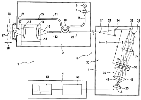
5 The LCDS apparatus 1 shown in Fig. 1 consists of a
measurement head 2, a scanning unit 3 and an electronic
unit 4. The representation is not to scale and is
strongly schematic. Constructive details which are not
essential for the function of the invention are not
10 shown .
The measurement head 2 and the scanning unit 3 contain
the optical components of a low-coherence interferometer
6. The light of a light source 7 is coupled via a lens 8
into a single-mode light conducting fiber which forms the
light source arm 9 of the interferometer 6. The primary
light transported in light source arm 9 is equally
divided by means of an optical coupler 10, acting as a
beam divider, as measurement light 16 into a sample arm
12 and, as reference light 22 into a reference arm 11, in
which arms the light transport also takes place inside
light conducting fibers. In the sample arm 12, the
measurement light 16 is coupled out by means of an
objective 13, composed of lenses 14 and 15. Lens 15
refocuses the measurement light 16 radiated through
aperture 17 towards a test specimen 18.
Both in sample arm 12 and in reference arm 11 a
reflection takes place, namely at a light-remitting site
20 of the measurement object 18 and at a reference
reflector 21, respectively. The reflected measurement
light 16 and the reflected reference light 22 are
recombined in optical coupler 10 and are transported as
detection light 24 in a detection arm 23 towards detector
25.
CA 02476174 2004-08-12
11
Up to this point, the construction of the interferometer
6 is essentially conventional and therefore needs not be
explained in more detail. Instead of the shown
interferometer device, another known configuration can
also be used. Especially, instead of the optical fiber
version using an optical fiber coupler 10, a free beam
arrangement with a free beam splitter can be used. In
principle, it is also possible to use separate optical
to elements as beam divider for light separation on the one
hand and~as beam uniting elements on the other hand.
Preferably, however, the same optical element 10 is used
for beam division and junction, as shown.
A specific feature of the interferometer device contained
in the measurement head 2 is that neither the reference
arm 11 nor the sample arm 12 contain means, by which the
lengths of both arms (generally expressed, the lengths of
the measurement light path and reference light path) are
changed relative to each other in order to vary the
longitudinal scan position along a scan section 27, shown
in dotted lines in Fig. l, in the scan direction
symbolized by arrow 28. Rather the variation of the scan
position, which is required to accomplish the
longitudinal scan, is produced by means of the scanning
unit 3 integrated into the light path of the detection
light 24, between the junction of the light (by means of
the optical coupler 10) and the detector 25.
Scanning unit 3 contains a variable wavelength selection
device, generally designated 30, whose essential
components may be seen more clearly in figures 2 and 3,
in two different embodiments. In the preferred case
shown, it comprises a spectral separation device 31, by
which the detection light 24 is spatially separated,
CA 02476174 2004-08-12
12
dependent on its wavelength ~. In the case shown, the
spectral separation device 31 is formed by a reflecting
spectral grating 32. However, also other optical elements
(transmission gratings, prisms), commonly used in
spectral devices may be chosen. Spectrally separated
light reflected from spectral grating 32 is focused onto
a spatial light selection device 38, by means of an
optical imaging system 36 which is composed of two
objectives 34 and 35. The first objective 34 collimates
to light emitted from entrance pupil 37 of the wavelength
selection device 30 onto the spectral separation device
31, while the second objective 35 focuses light emitted
from the spectral separation device 31 onto the light
selection device 38.
The spatial light selection device 38 has light passage
areas 39 and light blocking areas 40, alternately
disposed along a line, which preferably is straight and
extends in a spatial direction which is designated x in
2o the figures. In any case, the line of the alternating
light passage and blocking areas 39,40 must extend
transversally to the optical axis A of detection light
24, such that light which, dependent on its wavelength,
is spatially separated along the line by the spectral
separation device 31 strikes the alternating light
passage and blocking areas in such a manner that it is
transported towards the detector 25 with alternating
intensity, corresponding to the wavelength.
3o This may be achieved both with a transmission device,
shown in figure 2 and with a reflection device, shown in
figure 3. Detection light 24 passes through the light
passage areas 39 with less attenuation, as compared to
the blocking areas 40. For example, in figures 2 and 3,
light with wavelength ~1 striking the central section of a
CA 02476174 2004-08-12
13
light passage area 39 reaches detector 25 practically
without attenuation, whereas light with wavelength ~,2
centrally striking a blocking area is blocked nearly
completely. Light striking with wavelengths ~,3 between a
light passage area and a blocking area, is partially
attenuated. Based on figure 3, it becomes apparent that
the expressions "light passage area" and "light blocking
area" should not be understood, in a limiting manner, in
the sense of a transmission device where light passes
to through an optical element. On the contrary, the desired
alternating degree of attenuation may also be caused by a
reflecting optical element.
Figure 4 shows that in both cases of light selection,
i.e. the transmitting spatial light selecting device 42
according to figure 2, as well as the reflecting spatial
light selection device 43 shown in figure 3, the
transmission T and reflection R, respectively, of the
element varies, dependent on position x, preferably in
analog (especially sinusoidal) manner. Digital selection,
shown in figure in dotted lines is, however, also
possible. It is decisive that light selected according to
the defined k-profile of the wavelength selection device
is preferentially transported to the detector 25.
25 Preferably, the difference between the minimum light
attenuation of wavelengths corresponding to the k-profile
and the maximum light attenuation of the "blocked"
wavelengths ("selection contrast") should be as large as
possible.
According to the embodiments of the invention shown in
figures 1 through 3; the variable light wavelength
selection, in accordance with the k-profile of the
wavelength selection device 30, is achieved with a
constant angular dispersion of the wavelength-dependent
CA 02476174 2004-08-12
14
light separation, in combination with a variation of the
distance of the alternating light passage and blocking
areas 39,40 of the spatial light selection device 38.
Alternatively, it is also possible (and explained
hereafter, based on figure 11) to use a spectral
separation device 31 with variable angular dispersion in
combination with a constant spatial light selection
device 38. In principle, it is also possible that both
these elements are variable.
For example an electrically operated LCD mask may be used
as transmitting variable spatial light selection device
38 (figures 1 and 2). In this case, the minimum distance
of adjacent transmission areas is given by twice the
pixel distance of the mask. Larger distances may be
adjusted stepwise as multiples of this distance. An
approximately analog transmission variation may be
achieved if the pixel distance is much smaller than the
shortest desired distance between the transmission areas.
In this respect a reflection device of the type shown in
figure 3, where a DMD (Digital Mirror Device) can be used
as variable light selection device, is especially
advantageous. Such micromirror arrays are produced with
extremely small pixel distances, especially for
projection systems.
Hereafter, the principle used according to the invention
will be explained, based on figures 5 and 6.
Figure 5 shows, along a path ~z, the superposition of two
wave trains 45 and 46, oscillating in phase at the origin
(zero point). At the end of path ~z the wave trains are
again in phase, thus constructively interfering with each
other. It can be directly derived from the figure that
CA 02476174 2004-08-12
5
two wave trains interfere constructively under the
conditions shown, when their wavelength is an integer
fraction of Oz, i.e. when the condition ~ _ ~z/n
applies.
For the purpose of simplification, only two wave trains
were considered here. In reality, an interference of many
adjacent wave trains takes place. By considering the
correlation between wavenumber k and wavelength
to (k = 2 ~/~) the general rule may be derived that along a
path ~z those wave trains interfere constructively, whose
wavenumbers differ by
(1) ~k = 2 ~/Oz.
Such interference also takes places in the detection arm
of an interferometer. The origin zero point from which
path length ~z is measured, is defined by the point of
the measurement light path for which the optical path
lengths of the measurement light path and the reference
light path are identical. Hereafter, it will be
designated "point of coincidence of optical lengths". In
the context of the invention, the coincidence point is
significant in two ways:
30
a) On the one hand, it marks the point for which the
coherence condition explained further above is met.
In the common LCDS devices, this represents the basis
for longitudinal scanning.
b) At the same time, it marks the position at which the
measurement and reference light are in phase for all
wavelengths (provided there are no differences of
optical dispersion). The coincidence point is,
therefore, the zero point of the longitudinal scan
CA 02476174 2004-08-12
16
according to the invention. The actual scan position
is located at a distance 0z from the coincidence
point.
Figure 6 shows an interference spectrum resulting from
such a superposition (wavelength-depended intensity
normalized to the maximum value) in case of a light
source with a central wavelength ~o = 800 nm and a
spectral band width D~~H~ = 50 nm for an interference
1o path length ~z = 100 Vim.
Such a spectrum may be experimentally observed by placing
a reflector in the measurement light beam of a LCDS
device according to figure 1 at a distance 0z from the
coincidence point of the interferometer and by analyzing,
at the position of the spatial light selection device 38,
the intensity variation in x-direction along line 55,
i.e. the dependence of intensity upon the wavelength (by
means of a locally sensitive or displaceable detector).
2o The k-profile of the interferometer in the k-space
corresponds, for the chosen value of ~z, to this spectrum
in the ~-space.
From the above equation (1) a direct relation of the
distance of the maxima of the k-profile and ~z can be
derived mathematically. Consequently, in k-space the
points of maximum interference of the k-profile of the
interferometer are equidistant, as long as it is not
required to consider differences of optical dispersion
3o between the measurement light path and the reference
light path. Setting of a longitudinal scan position at a
distance Oz from the coincidence point is therefore
possible by setting the variable wavelength selection
device 30 to an equidistant sequence of wavenumbers k,
whose distances ~k are calculated in accordance with
CA 02476174 2004-08-12
17
equation 1. Since the correlation between ~ and k is not
linear (rather reciprocal) the corresponding spectrum in
~-space is not strictly equidistant. When considering a
relatively narrow band spectrum, as shown in figure 6 the
sequence of the selected ~-values is, however,
approximately constant, too.
As repeatedly mentioned, the preceding considerations are
based on the assumption that na optical dispersion has to
l0 be taken into account, i.e. the dependence of the
refractive index of the wavelength in the measurement
light path is the same as in the reference light path. In
commonly used LCDS devices, the spatial resolution of the
scan signal is negatively influenced by dispersion
differences. Therefore considerable efforts are usually
made to achieve, by an adequate choice of the light
conducting means, as much similarity of the optical
dispersion of both light paths as possible. In the
context of the present invention it is, however, possible
to offset in a simple manner the dispersion differences
between the light path of the measurement light 16 and
the light path of the reference light 22, by choosing the
sequence of the wavenumbers k which are selected by the
longitudinal wave selection device 30, deviating from an
equidistant sequence, in such a manner that the
difference in dispersion is offset. In other words, the
k-profile of the wavelength selection device is adapted
to the k-profile of the interferometer, which is not
equidistant, considering the dispersion. Experimentally,
this may take place in a relatively simple manner by
positioning a reflector in a plurality of different scan
positions on the scan path 27 and, for example as above
described, measuring the resulting spectrum in the
detection light path of the interferometer. According to
this procedure a k-profile of the interferometer is
CA 02476174 2004-08-12
18
obtained for each scan position within the Bz range. The
same k-profiles are also selected by the wavelength
selection device 30 and varied to accomplish a
longitudinal scan.
After passage of the wavelength selection device 30,
selected light 24 strikes the photosensitive surface of a
detector 25. The detector 25 is not locally selective,
i.e. it transforms the entire light intensity which it
1o receives into an electrical signal which is transferred
to the electronic unit 4, where it is evaluated.
According to the preferred embodiment shown in figures 1
to 3, a condenser lens 48 is arranged in front of the
detector 25, acting as light collecting element 49. It is
thus possible to capture, with a comparative small
detector surface, the entire light which passes through
the wavelength selection device 30.
Inside electronic unit 4, the intensity of light captured
2o by detector 25, is recorded by an evaluation unit 50,
dependent on the setting of the k-profile of the
wavelength selection unit 30. To each k-profile, the
corresponding value of the scan position ~z is allocated.
The intensity of the measurement signal, after deducting
a base line (i.e, the difference of the intensity from
the base line signal), corresponds to the intensity of
the reflection at the respectively selected scan
position.
Although scanning is not based on a modification of the
relation of the optical wavelengths of the measurement
light path (measured up to the coincidence point) and of
the reference light path, this does not mean that the
position of the reference reflector 21 in the reference
light path must be constructively fixed. On the contrary,
CA 02476174 2004-08-12
19
for the purpose of the alignment of the device, it can be
advantageous to make this position adjustable. During the
scanning procedure, however, the length of the reference
light path remains constant.
Figures 7 and 8 show two different embodiments of a light
selection device 38 which may be mechanically varied. A
common feature of both is that on a pivotable disc 54 and
56, respectively, light passage and blocking areas 39,40
1o are provided in the form of stripes which extend in such
a manner~that their stripe distance, measured along a
line 55 running across the disk surface, varies during
rotation of the disk. The light passage and blocking
areas may be produced in any desired shape, for example
by photo-lithographic processing of a metal-coated glass
plate.
In the case of the disk 54 shown in figure 7 the light
passage areas 39,40 are straight and parallel. A line 55
which is effective regarding the wavelength selection
(i.e. the line, upon which the spectrum of the spectral
separation device is projected) runs in such a manner
that the effective distance of areas 39,40 varies when
the disk 54 rotates.
In the embodiment shown in figures 8 and 8a, the light
passage and blocking areas 39,40 converge at a border
stripe 56 over sections of length 1 towards each other in
such a manner that their distance, relative to line 55,
3o upon which the spectrum is projected, decreases in each
segment 57 during rotation. During the passage of a
segment 57, a complete scan takes place, so that a very
high scan speed is achieved. For example, with a rate of
100 rotations per second and 100 segments 57 (with
replicated structures), a repetition rate of 10 kHz may
CA 02476174 2004-08-12
be achieved. Since the curvature of the line structure of
areas 39,49 may be chosen freely, it is possible to adapt
the light selection with respect to dispersion
differences of the measurement- and reference lights
5 paths.
In connection with figures 2 and 3, the possibility was
already described to utilize for the spatial light
selection device 38 an optical element (LCD, DMD) which
to allows selective setting of transmission or reflection in
different partial sections of its surface by electronic
means. Another example of this general principle is shown
in figure 9. In this case the detection light 24
originating from the spectral separation device 31 is
15 focused on the surface of an AOM (Acousto-Optical
Modulator). Inside the AOM, continuous sound waves are
generated. The resulting vibrations in the crystal (which
consists, for example, of TeOz) result in a spatial light
selection under an angle which corresponds to the first
20 order diffraction. Detector 25 and condenser lens 48 are
arranged at this diffraction angle relative to the
optical axis of light striking AOM 59. Contrary to the
earlier described embodiments, the light passage and
blocking areas 39,40 of the spatial light selection
device 38 formed by AOM 59 are not stationary on its
surface, but move continuously in x-direction. The
function of the invention is, however, not negatively
affected by this fact.
3o Figure 10 shows that the optical imaging function,
required in scanning unit 30, not necessarily has to be
provided by additional construction elements. For example
an arcuate spectral grating 60 may be utilized as a
spectral separation device 31. It provides not only the
spectral separation, but also the required collimation of
CA 02476174 2004-08-12
21
the light coming from the entrance pupil 37 onto the
spatial light selection device 38.
As already stated, figure 11 shows an alternative
embodiment of the variable wavelength selection device
30. Here a spectral separation device 31 with variable
spreading is used in combination with a constant spatial
light selection device 38. In this case the detection
light 24 coming from entrance pupil 37 and collimated by
objective 34 is spectrally separated by an AOBD (Acousto-
Optic Beam Deflector). The AOBD forms a variable spectral
grating having a grating distance which depends on the
applied electrical frequency. By means of the second
objective 35, the resulting spectral components are
focused upon a constant spatial light selection device
38.
Figure 12 shows a variable wavelength selection device 30
which is basically different from the earlier described
embodiments inasmuch as it is not based upon the
combination of a spectral separation device with a
spatial selection device. Here, detection light 24 coming
from the detection light guide 23 is coupled into a light
guide 64 with partially reflecting terminal faces having
a refractive index which depends on the electrical field
intensity. Photoconductor 64 is surrounded by two
electrodes 65, 66 to which a variable voltage V can be
applied in order to vary the electrical field strength
inside the photoconductor 64. Based on the Fabry-Perot
3o Effect, the alteration of the refractive index in
photoconductor 64 caused by the alteration of the
electrical field strength results in a variation of the
optical path which, in turn, causes a light wave
selection due to interference.