Note: Descriptions are shown in the official language in which they were submitted.
CA 02484791 2004-11-04
WO 03/105211 PCT/EP03/05658
- 1 -
Title of the Invention
Method for the Production of a Hetero-bipolar Transistor,
and Hetero-bipolar Transistor
Specification
The invention relates to a method for the production of a
hetero-bipolar transistor, as well as to a hetero-bipolar
transistor.
Hetero-bipolar transistors (HBTs), particularly in
composite semiconductor materials based on GaAs, typically
have a relief structure with an emitter shape designated as
a mesa, over a base layer, whereby the contacts for
controlling the base are spaced laterally at a distance
from the emitter mesa structure.
It is known that the long-term stability of the component
properties, particularly the current amplification, can be
significantly improved by means of passivation of the
semiconductor surface of the base layer, between the base
contacts and the emitter mesa, using a semiconductor
material that has been made to be weaker for carrying
charges. Such a passivation layer is referred to as a
ledge, both for HBTs in general and also in the following.
In this connection, the ledge generally consists of emitter
semiconductor material, and typically has a low layer
thickness; in the case of an emitter composed of several
semiconductor layers, it consists at least of the material
CA 02484791 2004-11-04
WO 03/105211 PCT/EP03/05658
- 2 -
of the emitter layer that immediately follows the base
layer.
A method is known, for example, from U.S. 5,298,439, in
which a lithographically structured metallic emitter
contact serves as a mask for ion-reactive anisotropic
etching of the emitter mesa, whereby a thin residual layer
of the emitter semiconductor material TnGaP having a
thickness of approximately 70 nm is left on the base layer,
which consists of GaAs, to the side of the emitter mesa.
In further lithographic steps, the structure of the ledge
is defined in this residual layer, whereby ion-reactive
etching methods (RIE) are used once again.
U.S. 5,668,388 describes a particularly advantageous layer
structure for the emitter of an HBT on GaAs, which takes
advantage of the highly selective etchability between GaAs
and InGaP in a layer sequence having several GaAs layers
and several InGaP layers. In particular, a first emitter
layer of InGaP having a layer thickness of approximately 30
nm is deposited on the GaAs base layer, and this is covered
by a GaAs layer having a thickness of only 5 nm, and then
additional InGaP and GaAs layers. In a first step, the
mesa structure is etched using an emitter metal contact
structured previously as an etching mask, down to the very
thin GaAs layer, whereby slight under-etching of the
semiconductor layers under the contact metal layer occurs.
Subsequently, the lateral structure of the ledge is defined
in a photoresist layer that is applied over the entire
surface, and the thin GaAs layer and the InGaP emitter
CA 02484791 2004-11-04
WO 03/105211 PCT/EP03/05658
- 3 -
layer are etched away in the regions not protected by the
photoresist.
A similar layer sequence with alternating GaAs and InGaP
layers is used as the basis in IEEE Device Letters, Vol. 17,
No. 12, p. 555-556, in order to etch the semiconductor
layers of the emitter back laterally under the metallic
emitter contact, by means of the alternating use of
selective etching agents, using wet chemistry, whereby a
-' ledge and an emitter mesa that is etched back further
laterally, relative to the former, are formed under the
masking metallic emitter contact. In this connection,
particular advantage is taken of the fact that GaAs also
forms a lateral etch stop for an enclosed InGaP layer. In
this method, the ledge is aligned relative to the emitter,
in self-adjusting manner, without any additional
lithography steps, whereby the adjustment of the lateral
dimensions causes problems because of the wet-chemical
etching processes that are repeatedly used. The metallic
emitter contact serves, at the same time, as a mask for
subsequent vapor deposition of contact metal for the base
contact. A self-adjusting alignment of the emitter contact
and the base contacts of an HBT is also known from EP 0 480
803 B1, where a defined distance between the emitter mesa
and the base contacts is adjusted by means of lateral
spacers on an emitter mesa. A lateral indentation in the
spacer layers prevents short-circuits between the emitter
contact and the base contact.
CA 02484791 2004-11-04
WO 03/105211 PCT/EP03/05658
- 4 -
The present invention is based on the task of indicating a
method for the production of an HBT (or a comparably
structured component) as well as an HBT particularly
produced according to such a method, having particularly
good long-term stability of the component properties.
Solutions according to the invention are described in the
independent claims. The dependent claims contain
advantageous embodiments and further developments of the
v invention.
The method according to the invention, with early
deposition of a passivation layer, results in advantageous
component properties, in that the passivation layer
deposited on the ledge reliably prevents damage to the
ledge layer, i.e. the interface of the ledge to the base
layer in subsequent process steps. The passivation layer
is structured and, with this structure, serves as a mask
for subsequent etching of the ledge. In this connection,
it is advantageous if this etching of the ledge is carried
out using a gentle isotropic, particularly wet-chemical
etching method, so that damage to the base layer that is
exposed in this process can be precluded. It turns out
that HBT components produced in this manner have a very
good long-term stability of the electric component
properties, in reproducible manner. The passivation layer
preferably remains on the ledge permanently, so that the
latter is reliably protected against damage during
subsequent process steps.
CA 02484791 2004-11-04
wo 03/105211 PcT/EP03/05658
- 5 -
It is advantageous to deposit nitride, particularly Si3N4,
on the ledge layer, i.e. in the case of a particularly
advantageous combination of the first emitter layer with a
semiconductor etch stop layer for the ledge region that
covers the former and can be selectively etched relative to
it, on this etch stop layer. Nitride adheres very well to
the semiconductor surface, so that no gap formation between
the semiconductor layer and the passivation layer occurs,
which could result in uncontrolled and/or non-uniform
-v etching of the ledge under the passivation layer. The
passivation layer can also consist of different materials,
preferably materials deposited in partial layers, one after
the other, for example in order to achieve more rapid layer
growth, for example of nitride and oxide, whereby
preferably the material that adheres better to the
semiconductor material, which is nitride in the example, is
deposited first, i.e-. directly on the semiconductor surface.
It is advantageous if the passivation layer is also
deposited on the vertical flanks of the mesa, for example
in an essentially isotropic process such as gas phase
deposition CVD, so that the structure of the mesa remains
uninfluenced by the etching of the ledge layer, which is
gentle on crystals and is wet-chemical etching, in
particular, and by the subsequent process steps.
Structuring of the passivation layer can take place, in a
first embodiment, using a mask produced by means of
photolithography which, at the same time, can serve as a
mask for producing metallic base contacts in a lift-off
CA 02484791 2004-11-04
WO 03/105211 PCT/EP03/05658
- 6 -
process. Preferably, however, a cover layer of the emitter
mesa, which particularly also serves as a first mask for
the structuring of the emitter mesa in a prior step, is
used as a second mask or as the basis for the second mask
for structuring of the passivation layer. The use of the
cover layer as a mask for structuring the passivation layer,
which in turn masks the etching of the ledge, has the
result that the semiconductor emitter mesa has a lateral
indentation under the cover layer, which essentially
- possesses the lateral dimension of the ledge. The use of
the structured cover layer for the first and the second
mask results in a particularly symmetrical and/or uniform
and precisely adjustable sizing of the ledge, because of
the self-adjusting alignment when using an essentially
anisotropic etching method, which proves to be particularly
advantageous for the long-term stability properties of the
components produced in this manner. According to an
advantageous further development, the space surrounded on
several sides by the cover layer, the semiconductor emitter
mesa, and the ledge, is permanently filled up with a
defined dielectric, particularly a polymer, preferably BCB
(benzocyclobutene), in order to prevent uncontrolled
deposition of materials from subsequent process steps.
A metallic emitter contact can serve as the cover layer, in
a manner actually known from the state of the art,
particularly in the embodiment having a second
photolithography mask. Preferably, however, the cover
layer is not formed by the metallic emitter contact, but
rather by a dielectric layer deposited on the latter,
CA 02484791 2004-11-04
WO 03/105211 PCT/EP03/05658
-
preferably an oxide, which remains essentially uninfluenced
by the subsequent etching steps, after the initial
structuring. The dielectric cover layer allows the
production of a lateral indentation by means of under-
etching, with particularly great precision, by means of
selective etching of the metallic emitter contact layer and
the structuring of the emitter semiconductor layers with
essentially the lateral structures of the metallic contact,
which is then only under-etched slightly in the
semiconductor layers. For this purpose, electrochemical
influences of the cover layers, which offer only the side
flanks as contact surfaces for a wet-chemical etching agent,
are minimized, for one thing. For another thing, as a
result of the automatic slow-down of the etching rate of
the emitter semiconductor layers when the lateral
structures of the emitter contact that serves as the
etching mask for the~emitter semiconductor layers, in this
regard, when these are etched, preferably by means of wet-
chemical etching, are reached, further under-etching of the
lateral structure of the metallic contact in the emitter
semiconductor layers can be kept very low, so that
variations of the lateral structure of the emitter
semiconductor layers due to an insufficiently controllable
etching rate or, in particular, due to a crystalline-
dependent etching rate, can be prevented or kept low, to a
great extent, and the lateral indentation determined by the
under-etching of the dielectric cover layer in the metallic
contact layer and therefore also the lateral expanse of the
ledge away from the emitter mesa can be precisely adjusted.
CA 02484791 2004-11-04
WO 03/105211 PCT/EP03/05658
_ g _
Depending on the layer structure of the emitter, it can be
advantageous to deposit a protective layer in an
intermediate step, particularly after the emitter
semiconductor mesa has been completed, to a great extent,
which layer protects the structure that has already been
etched from the renewed effects of the etching agent during
subsequent steps, and can be removed again before
deposition of the passivation layer. In an advantageous
embodiment, such a protective layer can be produced without
additional masking.
In the following, the invention will be explained in
greater detail, using preferred exemplary embodiments,
making reference.to the figures. These show:
Fig. 1 a first advantageous method sequence,
Fig. 2 a preferred method sequence,
Fig. 3 another advantageous method sequence.
In the following description of the exemplary embodiments,
the point of departure is a particularly advantageous layer
sequence, which is also already indicated in the document
U.S. 5,668,388 that was mentioned initially. In this
connection, the semiconductor layers 2 to 10 form the
vertical profile of an HBT on the GaAs substrate 1, whereby
2 represents the highly doped subcollector, 3 represents an
InGaP stop layer, 4 represents the collector having a low
doping, 5 represents the base, 6 represents the InGaP
CA 02484791 2004-11-04
WO 03/105211 PCT/EP03/05658
_ g _
emitter, 7 represents a very thin GaAs stop layer, 8
represents an InGaP stop layer, which can also be used as a
ballast resistor at an increased thickness, 9 and 10
represent the GaAs/InGaAs emitter contact, which ends in 10
with a highly doped InGaAs layer (Fig. la). After wet-
chemical pretreatment, the metallic contact layer 11 and
the contact reinforcement 12, which is also metallic, are
applied (Fig. 1b). Preferably sputtered diffusion barriers
such as WT1N, WSiN, TaN, or WTiSIN are used. The double
layer consisting of 11 and 12 should have a slight
mechanical bias, possess good adhesion properties on InGaAs,
and can preferably be structured in a plasma based on
fluorine. After deposition of the oxide layer 13, the
production of a first mask structure 13a in this oxide
layer takes place by means of the resist mask 14 (Fig. lc,
d), which structure subsequently masks the etching of the
metal layers 12 and il (Fig. le, f). As a result of the
lateral etching rates of the layers 11-13, which differ as
a function of the etching parameters, with low lateral
removal of the oxide 13a, the overhung structure shown in
Fig. 1f is formed. The lateral etching of the metallic
layers 11 and 12 is independent of direction and can be
well controlled, so that the dimension of under-etching can
be precisely adjusted. After the photoresist is removed,
the semiconductor emitter mesa in the layers 9 and 10 is
structured, preferably by a wet-chemical process (Fig. lg).
In this connection, the metal layers lla, 12a remain
essentially unchanged. This etching process takes place
selectively with regard to the InGaP layer 8, which is
retained over its entire area. In the case of the wet-
CA 02484791 2004-11-04
WO 03/105211 PCT/EP03/05658
- 10 -
chemical etching of the semiconductor layers 9 and 10, the
etching preferably proceeds significantly more rapidly
perpendicular to the layer plane than in the layer plane,
in known manner. Here, complete etching of the layers 9
and 10 in regions not covered by the metal layer 11 can be
reliably achieved by means of a predetermined time and/or
optical observation of the etching progress and, at the
same time, it can be guaranteed that the semiconductor
layers 9, 10 show only a slight further under-etching of
'9
-' the metal layer ll and essentially follow the precisely
adjustable lateral structure of the latter.
The flanks of the layers 9a and l0a of the emitter mesa,
which have been etched up to that point, are protected from
lateral etching attack by means of a photoresist mask 17 in
Fig. 1h, the lateral dimensions of which are not critical.
Subsequently, the InGaP layer 8 is etched using a wet-
chemical process, e.g. in HCl, selectively with regard to
the GaAs layers 7 and 9a, whereby the lateral under-etching
in the case of the InGaP etching is very high and the
protection layer 17 is greatly under-etched. The lateral
removal of the layer 8 automatically stops at the GaAs
layer 9a (Fig. li), however, in known manner. After
removal of the photoresist 17, a double layer consisting of
S1N and Si02 (15, 16) is applied isotropically, preferably
in a plasma deposition process (Fig. lj). This double
layer is removed in an anisotropic etching process, with
the cover layer structure 13b as a mask, which layer is
laterally broadened by the passivation layer 15, 16,
whereby no removal takes place under the overhang of 13b,
CA 02484791 2004-11-04
WO 03/105211 PCT/EP03/05658
- 11 -
so that the lateral structure indicated as 15a, 16a is
formed in the double layer 15, 16, above the semiconductor
layers 6, 7, the progression of which structure is
essentially dependent on the shape of the oxide mask 13a
with the broadened regions resulting from the passivation
layer 15, 16. By means of weakening the anisotropism of
this etching towards the end of the etching process, a
slight undercut of the oxide layer 16a in the nitride layer
15a that lies underneath it can occur. The GaAs layer 7
acts as a vertical etch stop. Subsequently, the structure
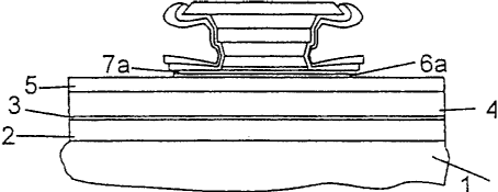
of 7a and 6a is etched from 6 and 7 (Fig. 11), using the
known methods for wet-chemical etching of GaAs and InGaP.
The etching preferably takes place selectively, in two
steps, whereby th,e GaAs layer 7 is removed in a first step,
and an undercutting of the mask 15a remains slight, because
of the very slight thickness of that layer. The etching of
the InGaP layer 8 preferably takes place by means of HC1,
so that the GaAs layer 7a again acts as a lateral etch stop.
The emitter is now in the region of 8a, while the region
outside of that is defined as a ledge. The ledge having
semiconductor layers 6a, 7a has a very uniform lateral
expanse relative to the mesa, as a result of this self-
adjusting production, relative to the emitter mesa, which
expanse is primarily determined by the initial under-
etching of the oxide mask 13a in the production of the mesa.
Fig. 2a starts from the process stage of Fig. lg. The
photoresist layer 17 shown in Fig. lh and li is replaced,
in Fig. 2b, with the photoresist spacer pieces 21 that are
produced in self-adjusting manner, as the protective layer.
CA 02484791 2004-11-04
WO 03/105211 PCT/EP03/05658
- 12 -
For this purpose, the photoresist is applied over the
entire area and exposed by means of flood exposure. The
oxide mask 13a is transparent for this exposure. By means
of the metal layers lla and 12a that overhang relative to
the semiconductor layers 9a and 10a, protection against the
exposure of the photoresist exists at the flanks of 9a and
10a, and after development, this has the result that the
photoresist remains on these flanks as a protective layer
(Fig. 2b). The photoresist spacer pieces 21 protect the
v InGaAs contact layer l0a from a lateral attack of the
concentrated HC1 during the subsequent etching of the InGaP
layer 8 (Fig. 2c). The further process sequence
corresponds to the above exemplary embodiment. The masking
of a protective layer that covers the semiconductor layers
9a, 10a, here the photoresist layer 21, by means of the
metallic contact layer, is generally particularly
advantageous for the-production of a protective layer at
lateral flanks of an emitter mesa.
In addition, it can be provided, after deposition of the
-' double layer 15, 16 as a passivation layer, to permanently
fill the cavity surrounded on several sides by the masking
structure 13a, the mesa layers 8 to 12, and the base layer,
i.e. the layers deposited on the latter, in defined manner,
with a dielectric, preferably the temperature-stable
polymer BCB (benzocyclobutene). BCB is spun on, for
example, in liquid form, solidified at an elevated
temperature, planarized (18 in Fig. 2d), and removed again
by means of etching outside of the cavity, so that a
permanent filling 18a of BCB remains. By means of filling
CA 02484791 2004-11-04
WO 03/105211 PCT/EP03/05658
- 13 -
the cavity, which step can also be inserted into the
process sequence according to Fig. 1, it is guaranteed that
no resist or chemical residues, which might influence the
component properties, remain in this region during later
process steps.
In the exemplary embodiment according to Fig. 3, in
deviation from the previous exemplary embodiment, the oxide
layer 13 is structured into the shape 13c, only slightly
larger than the planned lateral dimension of the emitter
semiconductor mesa, and under-etched in the metallic layers
12c, 11c as well as the semiconductor layers 10c, 9c, and
8c with only a slight lateral indentation, as illustrated
in Fig. 3a.
A passivation layer 15, preferably again consisting of
nitride, is applied over the entire area of this mesa
structure as well as the layer 7 that is exposed in this
connection. A photoresist mask 19 produced by means of
photolithography, which encloses the emitter mesa as a
second mask with lateral over-extension, is transferred
into the passivation layer 15 as a structure 15c, by means
of an anisotropic etching method (Fig. 3b).
As in the other exemplary embodiments, the structure 15c of
the passivation layer serves as a mask for producing the
ledge 6c, 7c in the semiconductor layers 6 and 7. In this
exemplary embodiment, the ledge structure is not self-
adjusting relative to the emitter mesa (Fig. 3c).
CA 02484791 2004-11-04
WO 03/105211 PCT/EP03/05658
- 14 -
A metal layer 20 is deposited over the entire area of the
structure according to Fig. 3c, in which the photoresist
mask 19 continues to exist unchanged, and the base layer 5
is exposed outside of the ledge, which layer forms the
metallic base contacts 20c on the semiconductor layer 5
(Fig. 3d). The base contacts reach right up to the
structure 15c of the passivation layer. The metal layer
deposited on the photoresist mask 20 is removed in a lift-
off process (Fig. 3c). For a clean lift-off process, the
photoresist mask 19 has a slight overhang and side flanks
that are drawn in, in a downward direction.
Tt is also advantageous if the structure 15a in the
passivation layer moves back slightly relative to the
vertical projection of the photoresist mask, which can be
achieved by means of weakening the anisotropism during the
etching of the passivation layer.
The characteristics indicated above and in the claims as
well as evident from the figures can be advantageously
implemented both individually and in various combinations.
The invention is not restricted to the exemplary
embodiments described, but rather can be modified in many
different ways, within the scope of the ability of a person
skilled in the art. In particular, different materials can
be used, other than the ones indicated as examples. If
different materials are selected, layers that are not
needed in terms of their function can be eliminated, and
other layers can be provided, in addition.