Note: Descriptions are shown in the official language in which they were submitted.
CA 02500479 2011-09-13
WO 2004/032254 PCTIUS2003/030696
-1-
ILLUMINATOR ASSEMBLY
Inventors: George W. Panagotacos, David G. Pelka, Roland Winston
BACKGROUND
The present invention relates generally and in various embodiments to
illuminator
assemblies. More specifically, the present invention relates generally and in
various
embodiments to illuminator assemblies including heat sinks.
Although various implementations of the present invention, among many, may be
described herein with reference to the specific illustrative embodiments
related to
particular applications, those skilled in the art will understand that the
invention is not in
any way intended to be, nor should be, limited to such embodiments and/or
applications.
Those having ordinary skill in the art and reference to the description of the
embodiments
disclosed and described herein will recognize that additional modifications,
applications,
and other embodiments may fall within the scope of the claimed invention, and
that there
may be additional fields in which the present invention may be practiced.
Compact sources of light are needed for a variety of applications in dentistry
and
surgery such as surgical cutting, curing of dental composite materials, and
activating
tooth-whitening materials, for example. Furthermore, dentists may use high
intensity light
for correcting diseases or defects in hard tissues such as the enamel and
dentin portions of
the teeth where drills are normally used. In other applications, for example,
dentists may
use high intensity light for curing a variety of resins and composites in a
patient's mouth
and for bleaching teeth. Dental composite curing and teeth bleaching
application
generally require sources of light that emit light having wavelengths in the
ultra violet
CA 02500479 2005-03-29
WO 2004/032254 PCT/US2003/030696
-2-
(UV) portion of the spectrum. Surgeons may use high power/high intensity
sources of
light in certain applications for correcting diseases or defects in soft
tissues for which
scalpels and other similar surgical cutting instruments are normally used.
Cutting
applications also may require sources of light that emit light having
wavelengths in
various portions of the spectrum.
Working in small confined areas such as a patient's mouth, for example,
requires
that the source of light be compact in size and highly maneuverable. Recent
advances in
solid state semiconductor technology in the field of laser diodes and light
emitting diodes
(LEDs) have enabled the miniaturization of these sources of light. Although
compact in
size, these solid state sources of light generally do not generate an adequate
amount of
power for the applications described above. When conventional solid state
sources of
light are driven with higher electrical input power to generate higher optical
output power,
thermal management becomes difficult and is an important obstacle to overcome
in order
to provide a source of light having enough intensity in optical output power
to make it
useful for certain dental and surgical applications, and other fields that may
require a high
intensity source of light for working in confined areas.
SUMMARY
In one general respect, embodiments of the present invention are directed to
an
apparatus that includes a lens having a light entrance end forming a recess, a
heat sink
having an end portion facing the recess, a light source positioned to transmit
light via the
recess into the lens in thermal communication with the heat sink, wherein heat
generated
by the light source is conducted to the heat sink.
In another general respect, embodiments of the present invention are directed
to a
method of providing optical radiation that includes providing a light source
that emits
light; using a heat sink member to stabilize the temperature of the diode
light source, the
heat sink member having an end portion facing a recess; transmitting light
from the light
source via the recess into a lens; transmitting heat generated by the light
source into the
CA 02500479 2005-03-29
WO 2004/032254 PCT/US2003/030696
-3-
heat sink; and delivering optical radiation through the lens having a light
entrance end
forming the recess.
In yet another general respect, embodiments of the present invention are
directed to
a method of treating a tooth that includes applying a tooth whitening material
to a tooth;
allowing the tooth to be exposed to the material in the absence of activating
light for a
substantial period of time; utilizing an array of diodes to produce activating
light having a
wavelength in the range 400-600 nm; emitting the light forwardly toward a
concave wall
defined by a lens; and applying the activating light to the material at a
power level of 100-
600 mW for a period of 20-40 seconds.
In still another general respect, embodiments of the present invention are
directed
to a method of curing a dental composite material, that includes applying a
dental
composite material to a tooth; utilizing an array of diodes to produce
activating light
having a wavelength in the range 400-600 nm; emitting the light forwardly
toward a
concave wall defined by a lens; and applying the activating light to the
dental material at a
power level of 100-200 mW for a period of 2-5 seconds.
Other apparatuses, systems, and/or methods according to embodiments of the
present invention will be or become apparent to one with skill in the art upon
examination
of the following drawings and detailed description. It is intended that all
such additional
apparatuses, systems, and/or methods be included within this description, be
within the
scope of the present invention, and be protected by the accompanying claims.
DESCRIPTION OF THE DRAWINGS
Embodiments of the present invention are described herein in conjunction with
the
following figures, wherein:
Figure 1 is a sectioned assembly view of one embodiment of an illuminator
assembly;
Figures 2 and 3 are side and end views, respectively, of one embodiment of a
lens;
CA 02500479 2005-03-29
WO 2004/032254 PCT/US2003/030696
-4-
Figures 4, 5, and 6 are side, end, and sectioned views, respectively, of one
embodiment of a lens holder;
Figures 7 and 8 are sectioned and end views, respectively, of one embodiment
of a
heat sink;
Figures 9 and 10 are side and end views, respectively, of one embodiment of a
heat
sink, Figure 9 showing wiring to LEDs, which are also shown in Figure 10;
Figures 11 and 12 are sectioned and end views, respectively, of one embodiment
of
a secondary heat sink;
Figure 13 is a sectioned view of one embodiment of the heat sink shown in
Figures
11 and 12;
Figure 14 is an end view of one embodiment of the heat sink shown in Figures
11,
12, and 13;
Figures 15 and 16 show one embodiment of a terminal board;
Figure 17 is an end view of one embodiment of a light source assembly showing
an LED array wiring configuration;
Figure 18 is an end view of another embodiment of a light source assembly
showing an LED array wiring configuration;
Figures 19, 20, and 21 show an end view, a sectioned view, and a side view,
respectively, of another embodiment of a terminal board; and
Figures 22 and 23 show a side view and an end view, respectively, of one
embodiment of an illuminator assembly.
DESCRIPTION
It is to be understood that the figures and descriptions of the various
embodiments
of present invention described herein, among others, have been simplified to
illustrate
representative elements of various embodiments of illuminator assemblies
comprising
various embodiments of light source assemblies that may be used in a variety
of
applications, such as, for example, applications requiring the use of high
intensity light
when working in confined quarters. The representative elements described
herein are
relevant for a clear understanding of the present invention. For purposes of
clarity,
CA 02500479 2005-03-29
WO 2004/032254 PCT/US2003/030696
-5-
however, other specific elements that would not facilitate a better or clearer
understanding
of the present invention may not be described herein. Those of ordinary skill
in the art
will appreciate, however, that these and other elements may be found in
conventional
illuminator assemblies and may be readily understood.
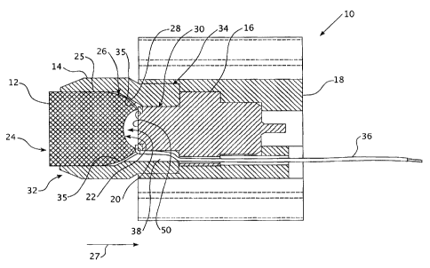
Figure 1 is a sectioned assembly view of one embodiment of an illuminator
assembly 10 in accordance with the present invention. The illuminator assembly
10 may
comprise a variety of components such as a lens 12, a lens holder 14, a first
heat sink 16,
and, optionally, a second heat sink 18, for example. The heat sink 16, 18 may
be any
substance or device for the absorption or dissipation of heat generated from a
process,
electronic device, or light source, for example. In one embodiment of the
present
invention, the lens 12 and the first heat sink 16 may be coaxially aligned. In
one
embodiment of the present invention, the first heat sink 16 and the lens
holder 14 also may
be coaxially aligned. In one embodiment of the present invention, the
illuminator
assembly 10 may include a housing 170 (e.g., see Figures 22, 23) extending
about the first
heat sink 16 and is in coaxial relation therewith. Further, the lens holder 14
may include
an end portion that is received into the housing 170. Also, in one embodiment
of the
present invention, the first heat sink 16 may act as a primary heat sink for
conducting heat
away from the light source while the second heat sink 18 may act as a
secondary heat sink
for conducting heat away from the first heat sink 16.
With reference to the embodiments depicted in Figures 1-23, the lens 12 may
include, for example, a light entrance end 20 forming a recess 22 and a light
exit end 24
where light generated by a light source assembly 50 (e.g., see Figures 9, 10,
17) located on
an end portion 30 of the first heat sink 16 is emitted. The lens 12 also may
include a
forward cylindrical portion 25 and a rearward portion 26 extending about the
recess 22
that defines an outer surface 28 that tapers in a direction 27 toward the
first heat sink 16
and/or the second heat sink 18.
The lens holder 14 may include a front portion 32 that extends about the
recess 22
of the lens 12 and may include a rear portion 34 for receiving the end portion
30 of the
CA 02500479 2005-03-29
WO 2004/032254 PCT/US2003/030696
-6-
first heat sink 16. Thus the end portion 30 of the first heat sink 16 projects
endwise into
the lens holder 14. The lens holder 14 also may define an inner wall 35 that
tapers in a
direction 27 toward the first heat sink 16 and/or the second heat sink 18. The
lens's
tapering outer surface 28 also may extend into the tapered portion of the lens
holder's
inner wall 35. The lens's outer surface 28 also tapers in the direction 27
toward the first
heat sink 16 and/or the second heat sink 18 and is oriented in adjacent
relation to the lens
holder's 14 inner wall 35.
The illuminator assembly 10 in accordance with one embodiment of the present
invention also may include a first current carrying wire 36 that extends
between the lens
holder 14 and the first heat sink 16 and/or the second heat sink 18. The first
current
carrying wire 36 may be used to supply electrical current to the light source.
The first
current carrying wire 36 may be received in an opening 38 formed in the lens
holder 14.
Figures 2 and 3 show a side view and an end view A-A, respectively, of one
embodiment of the lens 12 component of the illuminator assembly 10 according
to the
present invention. As discussed previously, the lens 12 may include, for
example, the
light entrance end 20 forming the recess 22 and the light exit end 24 for
emitting the light
generated by the light source assembly 50. As illustrated, the lens 12 has a
forward
cylindrical portion 25 and a rearward arcuate portion 26 that extends about
the recess 22.
The arcuate portion 26 defines an outer surface 28 that tapers in the
direction 27 toward
the first heat sink 16 and/or the second heat sink 18. In one embodiment of
the present
invention, the recess 22 may be re-entrant into the lens 12. The lens 12 may
include a
rearward wall 23 that is concave in a direction 21 toward the recess 22. In
one
embodiment of the present invention, the recess 22 may be filled with a light
transmitting
material, such as, for example, a light transmitting plastic material. For
example, the
recess 22 may contain an optical plastic material having a predetermined index
of
refraction. In one embodiment, the index of refraction of the optical plastic
material may
be substantially the same as the index of refraction as the lens 12 material.
Further, the
optical plastic material contained in the recess 22 may be curable by light
having a
CA 02500479 2005-03-29
WO 2004/032254 PCT/US2003/030696
-7-
wavelength in the ultra-violet (UV) portion of the optical spectrum, for
example. The lens
12, for example, may be a non-imaging lens and may be formed of a variety of
materials
such as optical polycarbonate, for example. In one embodiment of the present
invention,
the lens 12 may be a total internal reflection (TIR) lens.
Figures 4, 5, and 6 are side, end, and sectioned views, respectively, of one
embodiment of the lens holder 14 component of the illuminator assembly 10
according to
the present invention. The front portion 32 of the lens holder 14 defines a
first cavity 33
for receiving the light entrance end 20 of the lens 12. The front portion 32
and the inner
wall 35 of the lens holder 14 extend about the recess 22 of the lens 12. The
rear portion 34
of the lens holder 14 defines a second cavity 37 for receiving the end portion
30 of the first
heat sink 16 such that the end portion 30 of the first heat sink 16 including
the light source
assembly 50 projects endwise into the lens holder 14. The inner wall 35 of the
lens holder
14 tapers to a smaller diameter in the direction 27 toward the first heat sink
16 and/or the
second heat sink 18. The tapering outer surface 28 of the lens 12 extends into
the tapered
inner wall 25 portion of the lens holder 14. The outer surface 28 of the lens
12 is in
adjacent relation to the inner wall 35 of the lens holder 14 and is tapered
toward the first
heat sink 16 and/or the second heat sink 18. The lens holder 14 also defines
an opening 38
for receiving the first current carrying wire 36 therethrough. In one
embodiment of the
present invention, the lens holder 14 maybe formed of Teflon, for example.
Figures 7 and 8 are side and end views, respectively, of one embodiment of the
first heat sink 16 component, according to the present invention, where Figure
7 is a
sectioned view. The first heat sink 16 comprises a body portion 40, which may
include an
end portion 30 that faces the recess 22 portion of the lens 12. The end
portion 30 is
received into the second cavity 37 defined by the rear portion 34 of the lens
holder 14.
The end portion 30 also includes a face portion 31 for receiving the light
source assembly
50 (e.g., see Figures 9 and 10). In one embodiment of the present invention,
the face
portion 31 of the first heat sink 16 may be gold plated and/or gold/nickel
plated such that
the face portion 31 is rendered suitable for attaching a semiconductor die or
chip directly
CA 02500479 2005-03-29
WO 2004/032254 PCT/US2003/030696
-8-
thereon and is rendered suitable for accepting wire bonds thereon. For thermal
management purposes, the light source assembly 50 is placed in thermal
communication
or in contact with the body portion 40 or end portion 30 of the first heat
sink 16 and/or
with the second heat sink 18. Thus, the first heat sink 16 acts a thermal
conductor and its
body portion 40 conducts heat away from the light source assembly 50. The body
portion
40 of the first heat sink 16 also may transmit heat generated by the light
source assembly
50 to the second heat sink 18 formed about the first heat sink 16. The body
portion 40 of
the first heat sink 16 also may include a channel 42 formed therein for
receiving the first
current carrying wire 36 so that electrical current may be supplied to the
light source
assembly 50 located on the face portion 31 of the first heat sink 16. The body
portion 40
of the first heat sink 16 also may include an elongated portion 44, which may
define a
hollow portion 46 for receiving a second wire 48 (e.g., see Figure 9) therein.
The body portion 40 of the first heat sink 16 may be formed of a variety of
materials that are thermally conductive and/or electrically conductive
materials such as,
for example, aluminum, brass, bronze, copper, gold, nickel, platinum, steel,
and the like,
and/or any combinations of such materials including plated forms of such
materials. In
one embodiment, the first heat sink 16 may be nickel or gold plated copper. In
one
embodiment of the present invention, the first heat sink 16 may be nickel or
gold plated on
portions of the body 40 to make electrical connections. In other embodiments,
the first
heat sink 16 and the second heat sink 18 may be integrally formed.
Figures 9 and 10 are also side and end views, respectively, of one embodiment
of
the first heat sink 16 component according to the present invention. The first
heat sink 16
is shown wired to one embodiment of a light source assembly 50 according to
the present
invention. The light source assembly 50, may comprise, for example, a light
source 52
including a plurality or array of light emitting diodes 93 (LEDs) in
semiconductor die
form, and may be arranged in a predetermined manner as shown. The light source
assembly 50 is located on the face portion 31 of the first heat sink 16. The
light source
assembly 50 is positioned such that it faces the recess 22 formed on the light
entrance
CA 02500479 2005-03-29
WO 2004/032254 PCT/US2003/030696
-9-
portion 20 of the lens 12. Accordingly, the light emitted from the light
source 52 is
transmitted via the recess 22 and the material contained in the recess 22. In
one
embodiment of the present invention, the light source assembly 50 may comprise
one or
more LED semiconductor die(s) 93 die bonded to the face portion 31 of the end
portion 30
of the first heat sink 16. The light source assembly 50 also may include an
interface board
56 for making an appropriate physical electrical connection between a light
source power
supply and the light source 52. At one end, the first wire 36 is electrically
connected to
the interface board 56 at solder connection 58. At another end, the first wire
36 is
connected to a light source power supply. For example, the first wire 36 may
supply
electrical current to the light source 52 or may provide a return path (e.g.,
ground) for the
light source 52. The interface board 56 also may serve for receiving wire
bonds, e.g., from
the LED semiconductor dies 93.
A second wire 48 may be electrically attached to the elongated portion 44 of
the
first heat sink 16 by any well known means of attachment, such as a solder
connection 54,
a weld, screw, and the like. The second wire 48 also may be attached directly
to an outer
wall of the body portion as shown in Figure 9. In one embodiment of the
present
invention, the body portion 40 of the first heat sink 16 may be connected to
an electrical
connection of the light source assembly 50 through the second wire 48. The
electrical
connection may be used to supply power or a return path (e.g., ground) through
the second
wire 48. Those skilled in the art will appreciate, however, that the second
wire 48 may be
used as return signal or ground wire, without departing from the scope of the
present
invention.
The light source 52 may be coated with an optically transmissive encapsulating
material 60, such as UV curable adhesive optical acrylic material, for
example. In one
embodiment of the present invention, the encapsulating material 60 is placed
in a mold
such that its shape conforms to the surface contour of the recess 22 formed in
the light
entrance end 20 of the lens 12. Conforming the shape of the encapsulating
material 60 to
the contour of the recess 22 helps to transmit the light generated by the
light source 52 to
CA 02500479 2005-03-29
WO 2004/032254 PCT/US2003/030696
-10-
the lens 12 and through the light exit end 24 of the lens 12. The light source
assembly 50
will be discussed below in more detail with respect to Figures 15-21.
Figures 11 and 12 are sectioned and end views, respectively, of one embodiment
the second heat sink 18 component of the illuminator assembly 10 according to
the present
invention. Figure 13 is a sectioned view of the second heat sink 18 component
and Figure
14 is an end view thereof. The second heat sink 18 includes a body 62 having a
plurality
of fins 64 for conducting heat away from the first heat sink 16. The secondary
heat sink
body 62 defines an opening 66 for receiving the second wire 48 therethrough.
The
secondary heat sink body 62 also may define a passage or channel 68 for
receiving the
first wire 36 therethrough. The body 62 may be formed of a plurality of
thermally
conductive materials such as, for example, aluminum, brass, bronze, copper,
gold, nickel,
platinum, steel, and the like, and/or any combinations of such materials
including plated
forms of such materials. The materials may be the same or different form the
first heat
sink 16.
Figures 15 and 16 show a top view and sectioned view, respectively, of one
embodiment of the interface board 56 according to the present invention. The
interface
board 56 may comprise, for example, a substrate 57, which may be in the form
of a ring
defining an aperture or may have a shape that conforms to the face portion 31
of the first
heat sink 16. The substrate 57 may include, for example, an inner wall 70 and
an outer
wall 72. The substrate 57 may have a thickness 82 of about 0.025 inches, for
example.
In one embodiment of the present invention, the substrate 57 may be formed of
ceramic or any other material suitable for depositing metallic films thereon,
such as for
example, alumina, glass, silicon or other semiconductor, aluminum, copper,
gold, silver,
nickel, and the like. In one embodiment of the present invention, the
substrate 57 may
include a first metallic conductive film 74 processed on a top surface 76
thereof. In one
embodiment of the present invention the film 74 may be a thin film of gold, or
other metal,
suitable for wire bonding thereto, for example. The film thickness 80 may
range, for
example, from about 5 to about 10 microns. In one embodiment of the present
invention,
CA 02500479 2005-03-29
WO 2004/032254 PCT/US2003/030696
-11-
the top surface 76 of the substrate 57 may include a conductive pad 78 having
a second
metallic conductive film 79 processed thereon suitable for making a solder, or
other
electrical connection, thereto. Thus the conductive pad 78 may form an
electrical
connection between the first wire 36 and the interface board 56. The second
metallic
conductive film 79 may be, for example, a platinum silver paste having a
thickness
ranging from about 10 to about 16 microns, for example. The second metallic
conductive
film 78 may be suitable, for example, for attaching the first wire 36 to the
interface board
56 at a solder connection 58 for supplying electric current to the light
source 52, for
example. The first and second metallic conductive films 74, 79 may be
processed onto the
surface 76 of the interface board 56 by any one of a plurality of well known
methods for
processing such films, such as, for example, sputtering, vacuum deposition,
screen
printing and firing, and the like.
Figure 17 is an end view of one embodiment of the light source assembly 50,
shown in greater detail, including a nine up wiring configuration of the LED
array 52.
The LED array 52 comprises a plurality of LEDs semiconductor dies 93 die
bonded to the
face portion 31 of the first heat sink 16, for example. As discussed
previously, the face
portion 31 may provide a return path or ground connection to the power supply
for the
light source assembly 50. The interface board 56 also comprises the metallic
conducting
film 74 deposited on the surface 76 thereof. The metallic conducting film 76
may be
chosen for wire bonding any suitable type of wire bonds, such as, for example,
gold or
aluminum wire bonds. The LED semiconductor dies 93 may be wire bonded to the
top
surface 76 of the interface board 56 via wire bonds 94, for example. Electric
current may
be supplied to the LED semiconductor dies 93 via the wire bonds 94. The LED
semiconductor dies 93 may be interconnected to each other via wire bonds 96.
The LED
semiconductor dies 93 also may be connected to the face portion 31 of the
first heat sink
16 via wire bonds 98, for example. As shown, the LED array 52 is formed of
three banks
of LEDs 100, 102, 104, each comprising three LED semiconductor dies 93
interconnected
in series, for example. As discussed previously, the electrically conductive
wire 36 may
be connected to the interface board 56 through solder connection 58 and may be
used to
CA 02500479 2005-03-29
WO 2004/032254 PCT/US2003/030696
-12-
supply electric current to the light source assembly 50. The solder connection
58 may be
formed, for example, over the conductive pad 78 through the metallic
conducting film 79
deposited thereon. In one embodiment of the present invention the metallic
conducting
film 79 may be a palladium silver compound processed over the conductive pad
78, for
example.
Figure 18 is an end view of another embodiment of a light source assembly 110
comprising a light source 112 formed, for example, of one or more LED
semiconductor
dies 120, 122, 124. The light source 112 comprises a plurality of LED banks
114, 116,
118 in die form bonded to the face portion 31 of the first heat sink 16, for
example. Each
LED bank 114, 116, 118 may comprise one or more LED semiconductor dies 120,
122,
124 that emit light of a different wavelength. For example, the first LED bank
114 may
comprise an LED semiconductor die 120 that emits red light having an intensity
of up to
about 700 lumen, for example. The second LED bank 116 may comprise an LED
semiconductor die 122 that emits blue light having an intensity of up to 100
about lumen,
for example. The third LED bank 118 may comprise an LED semiconductor die 124
that
emits green light having an intensity of up to about 100 lumen. Those skilled
in the art
will appreciate, however, that embodiments of the present invention is not
limited to these
wavelengths and may include any combination of LED semiconductor dies 120,
122, 124
that emit light of any wavelength without departing from the scope of the
present
invention, including for example, LED semiconductor dies that emit amber light
having an
intensity of up to about 70 lumen.
As discussed previously the face portion 31 of the first heat sink 16 provides
one of
the electrical connections to the light source assembly 110. For example, in
one
embodiment of the present invention, the face portion 31 may provide a ground
connection or electric current return path to a light source power supply, for
example. The
light source assembly 110 also may comprise an interface board 126 including a
plurality
of individual wire bondable conductive pads 128, 130, 132, wherein each
individual
conductive pad 128, 130, 132 includes the metallic conducting film 74
deposited on the
CA 02500479 2005-03-29
WO 2004/032254 PCT/US2003/030696
-13-
surface thereof, for example, and the conductive film 74 is suitable for wire
bonding the
LED semiconductor dies 120, 122, 124 to the interface board 126. In one
embodiment of
the present invention, the three individual conductive pads 128, 130, 132 are
spaced 120
apart. Further, in one embodiment, the LED semiconductor dies 120, 122, 124
may be die
bonded to the face portion 31 of the first heat sink.
Electrical current may be separately supplied and separately controlled to
each
LED bank 114, 116, 118 through electrically conducting wires 134, 136, 138,
respectively.
Each wire 134, 136, 138 is connected to each conductive pad 128, 130, 132,
respectively,
via the solder connections 140, 142, 144, respectively. Therefore the relative
amount of
electrical current supplied to each LED bank 114, 116, 118 may individually
controlled so
that the relative light output intensity of each LED bank 114, 116, 118 may be
controlled.
Accordingly, the combined light output of each LED bank 114, 116, 118 may be
varied
through a wide range of wavelengths at various levels of intensity.
The individual LED semiconductor dies 120, 122, 124 forming any one of the LED
banks 114, 116, 118 may be interconnected to each other through
interconnecting wire
bonds 146. The first LED bank 114 may be connected to the conductive pad 128
via wire
bonds 148. Similarly, second and third LED banks 116, 118 may be connected to
conductive pads 130, 132 via wire bonds 150, 152, respectively. Each LED bank
114,
116, 118 may be connected to the face portion 31 of the first heat sink
through wire bonds
154.
Figures 19, 20, and 21 show a top view, sectioned view, and side view,
respectively, of another embodiment of an interface board 155 according to the
present
invention. In one embodiment of the present invention, the interface board 155
comprises
a substrate 157 in the form of a ring having an inner wall 156 and an outer
wall 158. In
one embodiment of the present invention, the substrate 157 may be formed of
ceramic or
any other material suitable for depositing metallic films thereon, such as for
example,
alumina, glass, silicon or other semiconductor, aluminum, copper, gold,
silver, nickel, and
the like. The substrate 157 thickness 160 may be about 0.04 inches, for
example.
CA 02500479 2005-03-29
WO 2004/032254 PCT/US2003/030696
-14-
In one embodiment of the present invention, the interface board's 155
substrate
157 may include a first metallic conductive film 162 processed on a top
surface 164
thereof. In one embodiment of the present invention the film 162 may be a thin
film of
gold, or any other metal, suitable for wire bonding, for example. The film
thickness 164
may be any thickness that provides sufficient electrical conductivity, such
as, a range from
about 5 to about 10 microns, for example. In one embodiment of the present
invention,
the top surface 164 of the substrate 157 also may include a conductive pad 166
having a
second metallic conductive film 168 processed thereon suitable for forming an
electrical
connection between any of the wires 36, 134, 136, 138 and the interface board
155
through the various solder connections 58, 140, 142, 144. The second metallic
conductive
film 168 may be, for example, a palladium silver paste having a thickness
ranging from
about 10 to about 16 microns, for example. The second metallic conductive film
168 may
be suitable, for example, for attaching any of the wires 36, 134, 136, 138 to
the interface
board 155 to provide electric current to the light source assembly 50, 110.
The first and
second metallic conductive films 162, 166 may be processed onto the surface
164 of the
interface board 155 using any one of a plurality of well known methods for
processing
such films, such as, for example, sputtering, vacuum deposition, screen
printing and firing,
and the like.
Figures 22 and 23 show a side view and a front view, respectively, of one
embodiment of a light source assembly 169 according to the present invention.
The light
source assembly 169 includes the lens 12, the lens holder 14, the first heat
sink 16, the
second heat sink 18, a housing 170, one or more standoffs 172, and a fan
assembly 174
including fan blades 176. The housing 170 extends about the first heat sink 16
and the
second heat sink 18 and is in coaxial relation therewith. The lens holder 14
has an end
portion received into the housing 170.
Embodiments of the present invention described above may be used in a variety
of
application such as, for example, processes for providing optical radiation.
This includes
providing the light source 52, 112 for emitting light of a predetermined
wavelength at a
CA 02500479 2005-03-29
WO 2004/032254 PCT/US2003/030696
-15-
predetermined intensity and using the first heat sink 16 or the second heat
sink 18 to
stabilize the temperature of the light source 52, 112. The first heat sink 16
may serve as a
heat sink member having an end portion facing the recess 20. The process also
includes
transmitting light from the light source 52, 112 via the recess 22 and into
the lens 12
portion. The first heat sink 16 conducts heat generated by the light source
assembly 50,
110 into the second heat sink 18. The optical radiation from the light source
52, 112 is
delivered through the lens 12 having a light entrance end 20 forming the
recess 22 and is
emitted through the light exit end 24 of the lens 12.
Furthermore, embodiments of the present invention also may be used to activate
tooth-whitening materials. For example, to whiten teeth, a tooth whitening
material is first
applied to the teeth. The teeth are then exposed to the material in the
absence of activating
light for a substantial period of time. The material is then exposed to light
having a
wavelength in the range 400-600 nm. The light is generated by the light source
52, 112
portion of the illuminator assembly 10 and is emitted forwardly toward the
concave wall
or recess 22 defined by the lens 12 and emerges from the light exit end 24 of
the lens 12.
The activating light may be applied to the material at a power level of 100-
600 mW for a
period of 20-40 seconds, for example.
Moreover, embodiments of the present invention may be used to cure dental
composite materials. For example, a dental composite material may be applied
to a tooth
and utilizing the light source 52, 112 comprising an array of LEDs 93, 120,
122, 124 to
produce activating light having a wavelength in the range 400-600 nm, for
example, the
material may be cured. The light may be emitted forwardly from the light
source 52, 112
toward a concave wall forming the recess 22 defined by the lens 12 at the
light entrance
end 20. In one embodiment of the present invention, the activating light may
be applied to
the dental material at a power level of 100-200 mW for a period of 2-5
seconds, for
example. In another embodiment of the present invention, the dental composite
material
may be a resin applied to a tooth.
CA 02500479 2005-03-29
WO 2004/032254 PCT/US2003/030696
-16-
Although the present invention has been described with regard to certain
embodiments, those of ordinary skill in the art will recognize that many
modifications and
variations of the present invention may be implemented. The foregoing
description and
the following claims are intended to cover all such modifications and
variations.
Furthermore, the components and processes disclosed are illustrative, but are
not
exhaustive. Other components and processes also may be used to make systems
and
methods embodying the present invention.