Note: Descriptions are shown in the official language in which they were submitted.
CA 02507177 2011-11-15
IMAGE PROJECTOR WITH FLEXIBLE REFLECTIVE ANALOG MODULATOR
FIELD F THE INVENTION
[0001] The present invention relates to an image projection system
comprising micromirror based light modulators, more specifically comprising at
least
one array of flexible reflective analog modulators (FRAMs) configured to
project a
bidimensional monochromatic or multicolour image.
BACKGROUND OF THE INVENTION
8 Light--find ieations-ina var. ety of elds-includin
projection displays for entertainment or training, printing, machine vision
and so on.
In particular, electrostatically actuated light modulators, otherwise known as
electrostatic light valves in the field of microelectrical mechanical systems
(MEMS),
may be used to control the propagation of light beams and the intensity
thereof in
various optical systems.
[0003] In most conventional systems, the light valves are comprised of
micromirrors whose surfaces are actuated between ON and OFF configurations
using digital ON/OFF actuation voltages applied thereon.
[0004] Generally, one of the ON or OFF configuration corresponds to a flat
micromirror surface, a high quality of which being quite difficult to achieve
and thus
explaining the difficulty in creating high quality systems based on such
conventional
light valve technology.
[0005] Furthermore, most conventional systems must generally operate with
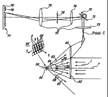
digital actuation voltages that provide static ON and OFF positions. As a
1
2612342.1
CA 02507177 2011-11-15
consequence, grey scale modulation levels potentially available through the
application of analog actuation voltages are not available in these systems.
[0006] Also, some conventional modulators generally provide a response time
which is too long for applications such as ultra-high resolution projection
systems.
[0007] Recently, a novel light modulator termed Flexible Reflective Analog
Modulator, hereinafter referred to as FRAM, has presented significant
improvements
over like modulators, namely in its ability to overcome some of the above and
other
drawbacks of conventional modulators. Consequently, the use and application of
these FRAMs in various optical apparatuses and systems have yet to be
addressed,
opening the possibility for a whole new realm of innovations in the fields
relying on
the use of light modulators, namely relating to optical intensity modulators
and image
projectors constructed on such technologies.
SUMMARY O THE INVENTION
[0008] It is therefore an aim of the present invention to provide a novel
optical
apparatus for modifying the divergence of at least one reflected beam, the
apparatus
comprising at least one Flexible Reflective Analog Modulator (FRAM).
[0009] It is also an aim of the present invention to provide a novel optical
system for modulating the light intensity of at least one reflected beam, the
optical
system comprising an optical apparatus for modifying the divergence of at
least one
reflected beam, and the apparatus comprising at least one Flexible Reflective
Analog
Modulator (FRAM).
[0010] It is a further aim of the present invention to provide a novel image
projecting system comprising an optical system for modulating the light
intensity of at
least one reflected beam, the optical system comprising an optical apparatus
for
modifying the divergence of at least one reflected beam, the apparatus
comprising at
least one Flexible Reflective Analog Modulator (FRAM).
2
2612342.
CA 02507177 2011-11-15
[0011] Therefore, in accordance with the present invention, there is provided
at least one flexible reflective analog modulator (FRAM), each said FRAM
generally
comprising a set of electrodes for applying an actuation voltage thereon and a
flexible reflective member of variable curvature for divergently reflecting an
input
beam therefrom to produce a reflected beam, said actuation voltage inducing an
electrostatic pressure on said flexible reflective member thus altering the
shape and
curvature of said member and inherently altering the divergence of said
reflected
beam.
[0012] Also in accordance with the present invention, there is provided an
optical apparatus for modifying the divergence of at least one reflected beam
comprising at least one light source generating at least one input beam, at
least one
FRAM, an illumination optics comprising at least one lens, said lenses
focusing said
input beams to produce at least one focused beam, said focused beams each
comprising a beam waist, each said FRAM having a FRAM position either in front
of,
behind or at one of said beam waists thus reflecting said focused beams
therefrom
and producing at least one reflected beam, the divergence of said reflected
beams
being determined by the position and curvature of said FRAMs, the latter being
controlled by an actuation voltage applied thereon, said actuation voltage
possibly
being modulated by a waveform that minimizes the FRAM response time.
[0013] Also in accordance with the present invention, there is provided an
optical system for light intensity modulation comprising the aforementioned
optical
apparatus for modifying the divergence of at least one reflected beam, and a
conversion optics for converting the variable divergence of said reflected
beams into
variable reflected beam intensities.
[0014] Further in accordance with the present invention, there is provided a
monochromatic image projector comprising the aforementioned optical system for
light intensity modulation coupled with a scanning mechanism and a projection
optics. For the operation of said image projector, said FRAMs are preferably
configured in at least one linear array, thus producing, when illuminated by
an
illumination optics designed to address said linear arrays, at least one line
of variable
3
2612342,1
CA 02507177 2011-11-15
intensity light dots. The lines of variable intensity light dots are then
scanned by said
scanning mechanism and projected through said projection optics to form a
bidimensional image.
[0015] Still further in accordance with the present invention, there is
provided
a monochromatic image projector, as described above, comprising an electronic
driver performing all FRAM driving functions, said FRAM driving functions
comprising
data processing, digital to analog conversion, waveform shaping, amplification
and
offset generation.
[0016] Still further in accordance with the present invention, there is
provided
a multicolour image projector comprising the aforementioned optical system for
light
intensity modulation coupled with a scanning mechanism and a projection
optics. For
the operation of said multicolour image projector, said light sources
preferably
comprise at least 3 laser light sources each operating at different
wavelengths, said
FRAMs being preferably configured in at least 3 linear arrays, thus producing,
when
illuminated by an illumination optics designed to address said linear arrays,
at least
one coloured line of variable intensity light dots. The coloured lines of
variable
intensity light dots are then combined and scanned by the scanning mechanism
and
projected through the projection optics to form a bidimensional multicolour
image.
[0017] Still further in accordance with the present invention, there is
provided
a multicolour image projector, as described above, comprising an electronic
driver
performing all FRAM driving functions, said FRAM driving functions comprising
data
processing, digital to analog conversion, waveform shaping, amplification and
offset
generation.
[0018] Accordingly, the present invention provides an optical apparatus
comprising at least one light source generating at least one input beam, at
least one
Flexible Reflective Analog Modulator (FRAM), said FRAM generally comprising a
flexible reflective member attached to a substrate by at least one leg
extending
outwardly therefrom, an electrode on said substrate and an electrode on said
flexible
reflective member thus forming a set of electrodes for applying an actuation
voltage
4
2612342.1
CA 02507177 2011-11-15
thereon, the optical apparatus further comprising an illumination optics
comprising at
least one lens, said lens focusing said input beam to produce at least one
focused
beam, said focused beam comprising a beam waist, said FRAM having a FRAM
position either in front of, behind or at one of said beam waist and a FRAM
orientation such that said focused beam is divergently reflected by said
flexible
reflective member of said FRAM to produce at least one reflected beam
therefrom.
[0019] The present invention also provides a light intensity modulator
comprising: an optical apparatus for variably modifying a divergence of at
least one
reflected beam comprising at least one light source generating at least one
input
beam, at least one Flexible Reflective Analog Modulator (FRAM), said FRAM
generally comprising a flexible reflective member attached to a substrate by
at least
one leg extending outwardly therefrom, an electrode on said substrate and an
electrode on said flexible reflective member thus forming a set of electrodes
for
applying an actuation voltage thereon, said FRAM having a natural FRAM
curvature
in the absence of an actuation voltage applied thereon defined by a natural
curvature
of said flexible reflective member, and a variable FRAM curvature adjusted by
a
range of actuation voltages applied thereon, said optical apparatus further
comprising an illumination optics comprising at least one lens, said lens
focusing
said input beam to produce at least one focused beam, said focused beam
comprising a beam waist, said FRAM having a FRAM position either in front of,
behind or at one of said beam waist and a FRAM orientation such that said
focused
beam is reflected by said flexible reflective member of said FRAM to produce
at least
one reflected beam therefrom, said reflected beam reflected by said FRAM
having a
variable reflected beam divergence dependent on the FRAM position and the
variable FRAM curvature of said FRAM, and thus on the range of actuation
voltages
applied thereon; and a conversion optics for converting the variable reflected
beam
divergence of said reflected beam into a variable reflected beam intensity.
[0020] The present invention further provides an image projector comprising:
an optical apparatus for variably modifying the divergence of at least one
reflected
beam comprising at least one light source generating at least one input beam,
a
2612342.1
CA 02507177 2011-11-15
plurality of independently operated Flexible Reflective Analog Modulators
(FRAMs)
organized in at least one linear FRAM array, said linear FRAM array comprising
at
least one FRAM, each said FRAM generally comprising a flexible reflective
member
attached to a flat substrate by at least one leg extending outwardly
therefrom, an
electrode on said substrate and an electrode on said flexible reflective
member thus
forming a set of electrodes for applying an actuation voltage thereon, each
said
FRAM having a natural FRAM curvature in the absence of an actuation voltage
applied thereon defined by a natural curvature of said respective flexible
reflective
member, a variable FRAM curvature adjusted by a range of actuation voltages
applied thereon, said optical apparatus further comprising an illumination
optics
configured to address said linear FRAM array, said illumination optics
focusing said
input beam to produce at least one focused beam, said focused beam comprising
a
beam waist, said FRAM array having a FRAM array position either in front of,
behind
or at one of said beam waist and a FRAM array orientation such that said
focused
beam is reflected by said flexible reflective members of said FRAMs of said
FRAM
array to produce a plurality of reflected beams therefrom, each said reflected
beam
reflected by a respective FRAM of said FRAM array having a variable reflected
beam
divergence dependent on the respective FRAM position and the variable FRAM
curvature of said respective FRAM, and thus on the range of actuation voltages
applied thereon; a conversion optics for converting the variable reflected
beam
divergence of each said reflected beam into a variable reflected beam
intensity, said
linear FRAM array of independently operated FRAMs thus producing at least one
line
of variable intensity light dots; and a scanning mechanism coupled to a
projection
optics, said scanning mechanism scanning through said at least one line of
variable
intensity light dots in a scanning direction perpendicular thereto, thus
projecting, in
conjunction with said projection optics, a bidimensional image.
BRIEF DESCRIPTION OF THE DRAWINGS
[0021] Having thus generally described the nature of the invention, reference
will now be made to the accompanying drawings, showing by way of illustration
a
preferred embodiment thereof, and in which:
6
2612342.1
CA 02507177 2011-11-15
[0022] Fig. IA is a graphical representation illustrating an approximate
variation of a reflected beam divergence with FRAM curvature for a micromirror
position zo = 0;
[0023] Fig. 113 is a schematic representation illustrating a FRAM intercepting
a focused beam, the FRAM being positioned at the beam waist of the focused
beam;
[0024] Fig. 2A is a graphical representation illustrating an approximate
variation of a reflected beam divergence with FRAM curvature for a positive
micromirror position, the dotted curve corresponding to the case zo=0 is
presented
here for comparison;
[0025] Fig. 2B is a schematic representation illustrating a FRAM intercepting
a focused beam, the FRAM being positioned in front of the beam waist of the
focused beam;
[0026] Fig. 3A is a graphical representation illustrating an approximate
variation of a reflected beam divergence with FRAM curvature for a negative
micromirror position, the dotted curve corresponding to the case zo=0 is
presented
here for comparison;
[0027] Fig. 3B is a schematic representation illustrating a FRAM intercepting
a focused beam, the FRAM being positioned behind the beam waist of the focused
beam;
[0028] Fig. 4 is a schematic representation illustrating a simplified system
for
converting the divergence variations of a FRAM-reflected beam into intensity
variations of same;
[0029] Fig. 5 is a schematic representation illustrating an improved system
for converting the divergence variations of a FRAM-reflected beam into
intensity
variations of same using a primary mirror of a Cassegrain system;
7
2612342.1
CA 02507177 2011-11-15
[0030] Fig. 6 is a schematic representation illustrating an optical system for
projecting a bidimensional image using linear FRAM arrays;
[0031] Fig. 7 is a graphical representation illustrating a simulation of a
FRAM
dynamic response to a 158V step function - structure dimensions = 25pm x 25pm,
mirror thickness = 0.15pm, mirror to substrate distance = 4.5pm;
[0032] Fig. 8 is a graphical representation illustrating a simulation of a
FRAM
dynamic response (FRAM dimensions as in Fig. 10) to an exponential voltage
variation with a time constant of 0.43ps;
[0033] Fig. 9 is a graphical representation illustrating a simulation of a
FRAM
dynamic response (FRAM dimensions as in Fig. 10) for decreasing exponential
voltage variations and a decreasing pressure ramp;
[0034] Fig. 10 is a graphical representation illustrating a simulation of a
FRAM dynamic response to OFF-ON switching with a two-step actuation waveform -
structure dimensions = 25pm x 15pm, mirror thickness = 0.1 pm, mirror to
substrate
distance = 2pm - two-step actuation parameters t1=0.275ps, P1=9kPa,
P2=15.5kPa;
[0035] Fig. 11A is a schematic representation illustrating the accelerated two-
step OFF-ON actuation function;
[0036] Fig. 11 B is a schematic representation illustrating the accelerated
two-
step ON-OFF actuation function; and
[0037] Fig. 12 is a block diagram illustrating of an electronic driver
designed
for the control of a FRAM array, wherein blocks with bold characters are part
of the
driver, while dotted blocks constitute comments.
DESCRIPTION OF THE PREFERRED EMBODIMENTS
[0038] Before proceeding with a detailed description of the present invention,
and to fully appreciate the utility of Flexible Reflective Analog Modulators
(FRAMs) in
8
2612342.1
CA 02507177 2011-11-15
same, it is important to review the basic optical and electrical principles
associated
with the use of FRAMs, and subsequently, in accordance with the preferred
embodiment of this invention, to discuss FRAM interactions with a focused
laser
beam, and other such light sources.
FRAM Basics
[0039] The FRAM, as disclosed in U.S. Pat. No. 7,088,493 to Alain et ai.,
generally comprises a thin flexible micromirror suspended over a substrate by
two
legs extending upwardly therefrom and hingingly supporting the micromirror at
opposite ends thereof. As will be apparent to a person of skill in the art, a
FRAM
structure may be constructed to include one, two, or more legs depending on
the
actual size and material properties of a given FRAM, possibly selected based
on the
specific use and application of the FRAM.
[0040] Generally, both the micromirror and the substrate comprise an
electrode for electrostatic actuation. The electrostatic actuation of the
FRAM, that is
by applying a voltage across the micromirror and the substrate electrodes, is
used to
control, for example, the curvature of the FRAM such that an optical beam
incident
thereon may be controllably reflected therefrom.
[0041] Illustratively, when an actuation voltage is applied between the
micromirror and substrate electrodes, an electrostatic force causes the
micromirror
to be pulled down towards the substrate thereby changing the form of the
mirror.
When the mirror is actuated, it can be curved inward to provide a concave, or
conversely convex, reflective surface. When the potential is released, the
mirror
returns to its rest position due to the restoring forces generated in the FRAM
structure, i.e. the material resilience of the micromirror and/or the
supporting legs.
Consequently, the application of a controllable potential to the substrate and
mirror
electrodes, for instance using a modulated analog or digital actuation
voltage,
provides a variably controllable mirror, for example defined by a variably
controllable
curvature.
9
2612342.1
CA 02507177 2011-11-15
[0042] The curvature of the unactuated FRAM, that is when no voltage is
applied thereon, is an important parameter that should be taken into account
for the
proper operation of the FRAM. This curvature is caused by the residual
internal
stress present in the FRAM structure. This internal stress can be controlled
through
fabrication parameters to achieve a determined residual curvature that can be
convex, associated with a compressive stress, or concave, associated with a
tensile
stress. In practice, the intermediate state corresponding to a flat mirror and
nominally
zero stress is very difficult to achieve. Typically, convex mirrors are
preferred as they
offer more flexibility for black level adjustment and a larger mirror stroke
that
potentially translates into better contrast in the image projection.
[0043] For the discussion on the operation of FRAM, the following definitions
are adopted. The FRAM curvature has its usual mathematical meaning, that is:
C = 1/R
where C is the FRAM curvature and R is the radius of curvature of the FRAM
optical
surface. R is positive if the center of curvature is located to the left of
the considered
optical surface when the illumination beam is incident from the right. With
this
convention for the radius sign, the curvature of a convex FRAM positioned for
reflecting an incoming light beam is positive. In the same position, a concave
FRAM
has a negative curvature.
FRAM Optics and Optical Systems
[0044] In accordance with a preferred embodiment of the present invention,
optical arrangements for modifying an incoming laser beam with a FRAM are
shown
in Figs. 113, 2B and 3B. In these configurations, a laser light source is used
as an
illumination source to generate an input beam 1. An illumination optics 2,
comprising
at least one lens 3 is used to focus the input beam 1, thus generating a
focused
beam 5, which is incident on a FRAM 4. The wavefronts of focused beam 5 may be
spherical, though alternative illumination optics 2 may be used to modify
input beam
1 to generate a focused beam 5 comprising cylindrical wavefronts which, in
general,
2612342.1
CA 02507177 2011-11-15
are used more efficiently in producing modulated light with the optical
arrangements
and systems described below, namely 2-D image projection systems. FRAM 4 can
be positioned either in front of (Fig. 2B), behind (Fig. 3B) or at (Fig. 1 B)
a beam waist
6 of focused beam 5 produced by illumination optics 2. In Figs. 1, 2 and 3, z
is
defined as a position along an optical axis 7 from beam waist 6, z being
positive
toward the illumination source.
[0045] Referring now to Fig. 4, input beam 1 is directed through illumination
optics 2, comprising at least one lens 3, generating a focused beam 5, which
is
incident on FRAM 4 at a position 19 along optical axis
7 either in front of, behind or at the beam waist of focused beam 5, thus
producing a
reflected beam 18 divergently reflected therefrom. In accordance with the
present
invention, when a gradually increasing voltage is applied to FRAM 4, the
curvature of
FRAM 4 changes, which inherently modifies the divergence of reflected beam 18
that
is being reflected therefrom. A divergent fraction 23 of reflected beam 18 is
defined
as the fraction of the reflected beam 18 diverging beyond the numerical
aperture of
illumination optics 2, and thus not being redirected back toward the light
source. A
returning fraction 24 of reflected beam 18 is defined as the fraction of the
reflected
beam 18 diverging within the numerical aperture of illumination optics 2, and
thus
being redirected back toward the light
source. Basically, the present invention proposes the use of the above
combination
of elements as an optical apparatus for modifying
the divergence of a reflected beam. Furthermore, by increasing the number of
FRAMs and/or the number of focused beams, the same apparatus may be used to
modify the divergence of a plurality of reflected beams. To support this
proposal, a
brief discussion of Gaussian optics as it relates to FRAMs, to focused laser
beams
incident thereon, and to reflected beams divergently reflected therefrom, is
presented
hereinafter.
[0046] Still referring to Fig. 4, Gaussian optics theory (Mouroulis P. and J.
MacDonald, "Geometrical Optics and Optical Design", Oxford University Press,
New
11
2612342.1
CA 02507177 2011-11-15
York, 1997) allows calculation of the divergence of reflected beam 18 as a
function of
the FRAM curvature:
0 = eo ICI [(2 z0 - 1/C)2 + (2 ZR)1
where 0 is the divergence of reflected beam 18, 8o is the divergence of
focused
beam 5, zo is the position 19 of FRAM 4 along optical axis 7 with respect to
the beam
waist of focused beam 5, and ZR defines the Rayleigh range of focused beam 5.
The
value of ZR is given by:
ZR = (TT W 2)/ A
where wo and A are respectively the size of the beam waist, and the
wavelength, of
focused beam 5. In the discussion below, the FRAM curvature matching the
wavefront of focused beam 5 for a given FRAM position zo is noted C,,,,(zo).
In that
specific case, reflected beam 18 is essentially indiscernible from focused
beam 5 as
the divergence of the former is identical to the divergence of the latter.
[0047] Fig. 1A graphically illustrates the variation of a reflected beam
divergence with FRAM curvature for a FRAM position zo of 0; with reference to
Fig.
I B, FRAM 4 is positioned at beam waist 6. In this case, Cwm(Zo) = 0,
representing a
flat mirror, which also corresponds to the curvature value for which the
minimum
reflected beam divergence is obtained. In this particular case where z0 = 0,
the
minimum reflected beam divergence coincides with the divergence 00 of focused
beam 5.
[0048] Fig. 2A graphically illustrates the variation of a reflected beam
divergence with FRAM curvature for a positive FRAM position zo > 0; with
reference
to Fig. 2B, FRAM 4 is positioned in front of beam waist 6. As can be seen,
with Z.
positive, the minimum divergence mn is smaller than 00 and is obtained for a
FRAM
curvature of Cwm(zo)/2. For curvature values 0 and Cwm(zo), the reflected beam
divergence coincides with the divergence 80 of focused beam 5. Referring now
to
Fig. 4, for a position 19 of FRAM 4 in front of the beam waist of focused beam
5, and
12
2612342.1
CA 02507177 2011-11-15
for FRAM curvatures 0 < C < CWm(zo), the divergence of reflected beam 18 is
inferior
to the divergence of focused beam 5, implying that reflected beam 18 could be
practically entirely redirected through illumination optics 2 in the direction
of the light
source; the return fraction 24 of reflected beam 18 in this case would thus
comprise
close to 100% of same. For FRAM curvatures above C,Nm,(zo) or below 0, the
divergence of reflected beam 18 is greater than the divergence of focused beam
5,
implying that reflected beam 18 can be discerned from focused beam 5, and the
divergent fraction 23 of the reflected beam 18 may be collected by a
conversion
optics 20, described below. This last condition will be discussed further in
association
with OFF and ON states of FRAM-based systems.
[0049] Fig. 3A is similar to Fig. 2A but with zo negative. In this case,
Cwm(zo) is
negative and, as for zo positive, the minimum divergence 8min is smaller than
80 and
is obtained for a FRAM curvature of CN,m(zo)/2. Again, for C = 0 and Cwm(zo),
the
divergence value is 80, and the same conditions will apply for FRAM OFF and ON
states. It is interesting to note that, in general, for a given position zo
other than 0 and
a given absolute value of a FRAM curvature, the divergence of a reflected beam
is
higher for a FRAM curvature with a sign opposite to the sign of z0.
[0050] Also as per the present invention, the aforementioned optical
apparatus for modifying the divergence of at least one reflected beam is
coupled to
conversion optics converting variations in the divergence of a reflected beam
into
variations in the intensity of same. This combination thus provides an optical
system
for light intensity modulation.
(0051] In Fig. 4, a simple configuration for accomplishing the above is
illustrated. As previously discussed, input beam 1, provided by a laser light
source in
a preferred embodiment of the present invention, is directed through
illumination
optics 2, comprising the at least one lens 3 providing focused beam 5 incident
on
FRAM 4. As mentioned above, for a
reflected beam divergence below a given divergence corresponding to the
numerical
aperture of lens 3, substantially all of reflected beam 18 is collected by
lens 3 and
13
2612342.1
CA 02507177 2011-11-15
propagated back toward the light source. The divergent fraction 23 is
practically null
and substantially no light reaches point A. This corresponds to a minimum
light
intensity and to a nominal black level. When the divergence is increased
beyond the
numerical aperture of illumination optics 2, the divergent fraction 23 of
reflected
beam 18 is collected by conversion optics 20, in this Fig. 4 comprised of
single lens
21, which focuses the divergent fraction 23 to the point A forming a single
light dot 22
(note that herein, the term light dot is meant to include any optical
convergence of
light into a point, which could be circular, oblong, square or have any other
shape).
The optical intensity of light dot 22 is inherently dependent on the optical
energy
confined to the divergent fraction 23 and thus to the divergence of reflected
beam 18,
which, as seen in Figs. 1A, 2A and 3A, is strictly dependent on the curvature
of
FRAM 4 and the position of same relative to the beam waist of focused beam 5.
Consequently, as the divergence of reflected beam 18 is gradually increased
beyond
the numerical aperture of lens 3, so is the intensity of light dot 22 at point
A.
[0062] Tho above example is quite simple and inefficient. Other, better and
more efficient optical systems exist to perform the same type of conversion
(Cassegrain optics, Schlieren optics, mask arrangements combined with optics,
etc...). Fig. 5 gives an example of such a system based on Cassegrain optics.
An
input beam 1, provided by a laser light source in a preferred embodiment of
the
present invention, is directed through an illumination optics 2, again
comprised of a
single lens 3, providing a focused beam 5 incident on a FRAM 4 at position 19
along
optical axis 7 either in front of, behind or at the beam waist of focused
beam 5. Again, when the divergence of reflected beam 18 is increased beyond
the
numerical aperture of lens 3, divergent fractions 23 of reflected beam 18 are
collected by a conversion optics 40, this time comprising a Cassegrain system
primary mirror 41 and a focusing lens 42, wherein the primary mirror 41
redirects
divergent fractions 23 into collimated beams 45, which are ultimately focused
by lens
42, with resulting beams 46 converging from lens 42 to a point B forming a
single
light dot 47 of variable/adjustable intensity.
14
2612342.1
CA 02507177 2011-11-15
[0053] Without affecting significantly the generality of the present
discussion,
it can be assumed that the optical system converting divergence change into
light
intensity modulation is such that a low divergence corresponds to a low light
intensity. A person of ordinary skill in the art will understand that a
similar system
may also be developed wherein the converse is true, that is wherein a low
divergence corresponds to a high light intensity. Such systems may also be
used in
the above and following examples without extending the general scope and
nature of
the present disclosure.
[0054] The above-described optical systems, wherein for instance a low
divergence corresponds to a low intensity, generally exhibit a divergence
threshold
below which the produced light intensity is low and substantially constant.
This
intensity corresponds to the nominal black level of the optical system. When
the
divergence produced by the FRAM is above the threshold, the light intensity
increases steadily with the absolute value of the FRAM curvature. The
divergence
threshold should be such that it is possible to position the FRAM to produce
divergence values below the divergence threshold for a range of FRAM curvature
values. This allows the realization of a high quality black level.
Simultaneously, the
divergence threshold should be kept as small as possible to maintain the
optical
system energetic efficiency as high as possible. When both conditions for the
divergence threshold selection are fulfilled, it can be seen from Figs. 2A and
3A that
in the cases with zo 0 0 and for a given threshold, there is a larger
curvature range
for which the obtained divergence is below the threshold than in the case of
zo = 0.
This translates into a lower sensitivity of the nominal black level adjustment
to the
FRAM curvature and associated actuation voltage. This lower sensitivity of the
black
level adjustment in the cases with zo * 0 has also an impact on the optical
settling
time of the black level. In general, as soon as the FRAM mechanical
oscillations
around the equilibrium position for the black level correspond to curvature
values
within the range for which the obtained divergence is below the threshold, the
black
level is stabilized. Therefore, the black level settling time is typically
shorter for a
larger curvature range with corresponding divergences below the threshold.
This
means that the black level optical settling time for cases with zo 0 0 is
generally
2612342.1
CA 02507177 2011-11-15
shorter than for the case of zo = 0. In the particular case where the
divergence
threshold of the optical system is between 0o and 0mi, it is not possible to
obtain a
high quality black level with zo = 0; parameter zo must be different than 0.
It is
interesting to note that the presented scheme for light modulation does not
rely on an
optically flat micromirror state to produce the nominal black level, a common
feature
of conventional systems. This is an important advantage since such a flat
mirror
state is difficult to obtain in practice.
[0055] Up to this point, the discussion was restricted to optical arrangements
comprising a single FRAM, namely an optical apparatus for modifying the
divergence
of a reflected beam and a light modulating system comprising the optical
apparatus
and an appropriate conversion optics for converting variations in divergence
into
variations in intensity. Therefore, also in accordance with the present
invention, the
aforementioned FRAM-based light modulating system is modified to comprise at
least one linear array of FRAMs instead of a single FRAM. In this FRAM array-
based light modulating system, the FRAMs are coupled with appropriate
illumination
and conversion optics to produce at least one line of light dots whose
intensities are
modulated according to the actuation voltages applied to each FRAM
individually.
For this configuration, the light beam illuminating the linear FRAM arrays can
no
longer be composed of a single spherical wavefront train, as generated by an
illumination optics comprising a single lens, such as described in Figs. 4 and
5.
[0056] Referring now to Fig. 6, there is defined appropriate illumination
optics
52 that can modify the wavefront of an input beam 1 to properly address a FRAM
array 54 at a position 59 along optical axis 7 in front of, behind or at an
effective
beam waist of a focused beam 55. For simplicity, this example will be limited
to the
illumination of FRAM array 54 comprising a single linear FRAM array 54'. One
option
is to select the illumination optics 52 such that it produces focused beam 55
comprising cylindrical wavefronts. In practice, the focused beam 55 with
cylindrical
wavefronts would be represented by a narrow line of light illuminating FRAM
array
54. Another option is to illuminate FRAM array 54 with focused beam 55
comprising
an array of spots, one light spot corresponding to each FRAM 4 of FRAM array
54.
16
2612342. 1
CA 02507177 2011-11-15
To generate such an illumination pattern from a single Gaussian beam emitted
by a
laser, illumination optics 52 would comprise either an appropriate diffractive
optical
element or a microlens array. In each of the above examples, each FRAM 4 of
FRAM array 54 would divergently reflect a respective fraction of focused beam
55,
generating a plurality of reflected beams 58, the divergence of each reflected
beam
being dependent on a respective FRAM curvature and position. Reflected beams
58
of divergence greater than the numerical aperture of illumination optics 52
will each
comprise a divergent fraction 63 to be converted into a reflected beam
intensity, and
thus a visible light dot at point C, by appropriate conversion optics 60.
Reflected
beams of divergence lesser than the numerical aperture of illumination optics
52 will
not be collected by conversion optics 60 and will thus generate, in practical
terms, a
black level light dot at point C. The combined reflected beams will thus
generate a
line of variable intensity light dots at point C.
[0057] Still in accordance with the present invention, an image projector
comprises the combination of the FRAM array-based light modulating system,
with a
scanning mechanism and a projection optics. Still referring to Fig. 6, the
light
modulating system described above is coupled to a scanning mechanism 70, in
this
example comprising a single flat mirror scanner 71, and projection optics 72,
here
comprising lenses 73, 74 and 75, capable of displaying a 2-D image 76 on a
screen
77. The line of light dots (i.e. pixels) of variable intensities produced at
point C by
FRAM array 54, the FRAM array 54 still comprising one linear FRAM array 54',
is
scanned across screen 77, in a scan direction 78 perpendicular to the line of
light
dots, through projection optics 72. The information controlling the actuation
voltage
of each FRAM 4, and therefore the intensity of each light dot at point C, is
updated
for each displayed line throughout the scan process. This produces a 2-D image
76
composed of light dots of variable intensity. Due to the typically short
response time
of the FRAMs, namely below 5 ps, the resulting system allows display of
thousands
of image lines at high a frame rate.
[0058] Necessarily, the above configuration, when comprising a single laser
light source, provides a monochromatic projection system. Another embodiment
of
17
2612342.1
CA 02507177 2011-11-15
the present invention comprises an immediate extension of this monochromatic
projection system. In general, a multicolour projection system can be achieved
by
using at least two laser light sources operating at different wavelengths. For
instance,
three light sources operating at different wavelengths and thus providing
three
coloured beams possibly of colours red, green and blue, could be used in a
multicolour projection system to provide most colours in the visible spectrum.
For
example, still referring to Fig. 6, a multicolour projection system comprises
three
conversion optics 60 adapted to address the divergent fractions 63 of three
reflected
beams 58 of different colors, each controlled by respective FRAM arrays 54'.
The
latter are positioned at respective positions 59 along optical axis 7 either
in front of,
behind or at the effective beam waists of respective focused beams 55. Each
coloured beam is directed by an appropriate illumination optics 52 to a
respective
linear FRAM array 54' to produce, in conjunction with an appropriate
conversion
optics 60, at least one line of light dots of a given colour. The three lines
of light dots
of different colours are then combined and propagated toward a scanner and a
projection optics to produce a 2-D colour image on screen 77.
[0059] As will be apparent to a person of ordinary skill in the art, other
optical
setups and system configurations can be applied to the systems presented
herein
without departing from the general scope and nature of the present disclosure.
For
instance, many other types of illumination optics, conversion optics and
scanning/projection mechanisms may be considered to provide a similar result.
Furthermore, other light sources may be used to replace the laser light
sources
described herein. It will be readily understood that the FRAM systems can be
designed to benefit from the great versatility and applicability of the FRAM
technology to develop various optical solutions unavailable with conventional
light
valves.
FRAM Actuation Voltage Waveforms and Electronics
[0060] In a preferred embodiment of the present invention, the actuation
voltages applied individually to each FRAM of a FRAM array are modulated by an
electronic driver, specifically designed for the control of the FRAM array,
using
18
2612342.1
CA 02507177 2011-11-15
predetermined waveforms to reduce the response time of each FRAM. Reduced
response times inherently improve the frame rate and resolution of the
aforementioned monochromatic and multicolour projection systems.
[0061] To illustrate the effectiveness of such actuation waveforms, dynamic
response simulations of various FRAM microstructures under the influence of
various
actuation voltage waveforms are presented hereinbelow. Though the illustrated
results of the following discussion refer to simulated FRAM responses to
various
actuation voltages, experimental results have also been obtained for similar
actuation
conditions to support the following. For instance, experimental FRAM responses
to
ramp-like actuation voltages, as will be discussed further with reference to
the
simulated results of Fig. 9, confirm the impact of such actuation voltage
waveforms
and their ability to improve the responsiveness and accuracy of FRAM-based
systems.
[0062] Referring first to Fig. 7, a simulation of the response of a FRAM
microstructure to a voltage waveform in the shape of a simple step function
shows
that the FRAM microstructure is clearly underdamped; simulations were
performed
for a 25pm x 25pm micromirror structure with a mirror thickness of 0.15pm and
an
electrode-to-mirror gap of 4.5pm. This causes the FRAM to overshoot and
oscillate
around its equilibrium position for a relatively long time. The FRAM
stabilization time
is a critical parameter for projection applications due to its effect on the
achievable
resolution in the scan direction. Alternate voltage waveforms can be used to
minimize the oscillations of the FRAM.
[0063] Various voltage waveforms, inherently corresponding to electrostatic
pressure waveforms since the electrostatic pressure is proportional to the
square of
the voltage, can be used to reduce the FRAM settling time. For example,
exponentially varying voltage waveforms have been investigated. Such waveforms
are mathematically described as:
V=Va(1-e t/T) (0 pm to maximum deflection: actuation)
V=Vo e -t/' (maximum deflection to 0 pm: deactuation)
19
2612342.1
CA 02507177 2011-11-15
where T is the time constant of the exponential waveform and Va the voltage
required
to reach a specified micromirror curvature. Simulations using such exponential
waveforms to activate a FRAM, of same structure dimensions as that studied in
Fig.
7, are presented in Fig. B. These results indicate that it is possible to
reduce the
FRAM oscillations significantly by selecting the time constant of the
exponential
waveform carefully. For the structure considered, a time constant of 0.43 Ns
achieves settling times typically shorter than 5 ps and even times below 2 ps.
These
dynamic results were obtained for mirror actuation. When the inverse case is
considered (mirror deactuation), it becomes more difficult to reduce mirror
oscillations using pressure variations corresponding to an exponentially
decreasing
voltage since pressure is a non-linear function of applied voltage. For the
same
structure, activated with a voltage decreasing exponentially with a time
constant of
0.43 ps (see Fig. 9), the settling time is about 9 ps. If the time constant is
increased
to 3.26 ps, the settling time decreases to 5.3 ps which is similar to the
settling time of
a mirror actuation obtained with a time constant of 0.43 ps.
[0064] The dynamic response of a FRAM, of same structure dimensions as
that studied in Fig. 7, to a decreasing electrostatic pressure ramp of the
form:
P=Po(1-t/6),0<t<O
P=O, t?b
which corresponds to a voltage waveform of the form:
Voc Po112 (1-t/6)112 0< t < b
V=O, t >_b
where Po is the initial pressure and b the ramp duration, is also presented in
Fig. 9
using 6=2 ps. This indicates that this type of pressure variation is effective
in
reducing the FRAM oscillations if the ramp duration iS is carefully selected.
In the
example shown, the time required to stabilize the FRAM is as short as 2.6 ps.
As
2612342.1
CA 02507177 2011-11-15
stated hereinabove, experimental results applying such ramp-like actuation
voltage
waveforms also support these simulated results.
[0065] Another way to limit the oscillations of the FRAM is to take advantage
of the speed reduction occurring each half period of the FRAM oscillation.
This leads
to the so-called two-step function actuation described below. At t= 0, a first
step
function is applied with a pressure load P1 selected to achieve FRAM overshoot
down to the target equilibrium position zeq. At time t1, defined as the time
corresponding to the FRAM displacement zeq, the velocity is null. A second
step
function is then applied with a pressure load P2 providing static equilibrium
at zeq.
Because at t1 the electrostatic force is made equal to the restoring force,
the
equation for the FRAM dynamics becomes mi = 0 with initial conditions z(t,) =
0
and z(t1) = zeq. This leads to z(t) = zeq. Ideally, after t1, the structure is
stopped at the
target position. Simulations were performed for a 25pm x 15pm
micromirror.structure
with a thickness of 0.1 pm and an electrode to mirror gap of 2 pm (see Fig.
10). In
this case, P1 = 9 kPa and t1 = 0.275 ps. The stabilization is reached after
0.29ps.
Almost no oscillations are observed in this example.
[0066] A modified version of the two-step actuation function, the so-called
accelerated two-step function, can also be used. The principle here is to
accelerate
the FRAM by applying a larger pressure P, during a time t', shorter than t,.
The
deceleration down to zeq, is still due to the restoring and damping forces.
Figs. 11A
and 11 B present the schematic diagrams of z(t) and P(t) for this type of OFF-
ON and
ON-OFF actuation waveforms, respectively. The accelerated two-step function
requires the application of a high voltage but this voltage can be fixed while
t', only is
varied. Only the range of the pressure P2 needs to have a high resolution and
it
remains the same for all types of actuations because it determines the
precision of
the equilibrium position. This actuation function provides potentially shorter
response
times and the same theoretical advantages as the two-step function.
[0067] Another possible actuation waveform worth mentioning is a filtered
step function. The filter applied to the step function eliminates frequencies
21
2612342.1
CA 02507177 2011-11-15
corresponding to the lower resonant frequencies of the device from the step
function
spectrum. This is effective in reducing the energy coupled into the preferred
oscillating modes of the device, which, in turn, minimizes overshoot, unwanted
oscillations and response time.
[0068] Besides providing the appropriate actuation waveform to minimize the
FRAM response time, the electronic driver powering and controlling the FRAMs
must
perform a set of functions essential to its proper operation. It must be
possible to
apply an offset voltage to FRAM micromirrors to adjust their low voltage
curvature. A
coarse offset voltage can also be applied to the common electrode located
underneath all the micromirrors, thus generating an identical coarse offset
value for
all the micromirrors in the array. It must also be possible to select a fine
offset value
for each individual micromirror to be directly applied thereon. This way, the
total
offset value for each micromirror may be adjusted to correct for possible
irregularities
arising from micromirror to micromirror. The individual offset values result
from a
calibration procedure and can be loaded in the driver circuit only once before
operating the FRAMs. The actuation voltage values corresponding to the
required
grey levels are added to the individual offset values and applied on each
micromirror.
A high actuation voltage resolution of at least 11 bits is required to allow
for the
implementation of data processing algorithms that correct for the gamma
function
and for the irregularities among mirrors. The data set activating the FRAM
array
must be refreshed simultaneously for all micromirrors up to 300,000 times per
second. In the context of 2-D image projection, this would allow the display
of up to
5000 image lines at a frame rate of 60 Hz. As already mentioned, features (for
example, selectable time constant for exponentially varying actuation voltage)
must
be included to the electronic driver to provide some flexibility in adjusting
the
actuation waveform shape to minimize the micromirror overshoot and settling
time.
[0069] Fig. 12 presents a block diagram summarizing the features of an
electronic driver specifically designed for the proper control of a FRAM array
in
accordance with the present invention. The data carrying the information
required to
generate the light intensity pattern, as well as the calibration data of the
system in
22
2612342.1
CA 02507177 2011-11-15
question, is fed through a data processing algorithm which computes the
actuation
voltage to be applied to each FRAM, taking into account the gamma function,
the
mirror irregularity correction determined during calibration, the individual
offset
required of each mirror, and waveform shaping. The digital data, coded at a
high
resolution, namely 11 bits or more, and processed for a high mirror data
refresh rate,
namely in the range of 300kHz, is converted to an analog voltage of
appropriate
waveform, which is further amplified before being applied to the FRAM array.
Additionally, the calibration data of the system is utilized to set a static
coarse
voltage offset to all FRAMs. Ultimately the fully calibrated and optimized
FRAM
based image projector will be able to produce up to 5000 colour image lines at
a
frame rate of 60Hz.
[0070] As presented herein, FRAM-based optical systems can be used in a
variety of applications. Namely, the use of FRAMs to provide accurately
controlled
light modulation, for instance in high-resolution projection systems, can be
highly
beneficial over the use of conventional light valves.
[0071] For example, the simple construction of the FRAMs renders FRAMS
easy and less costly to produce. Furthermore, the rapid response time of the
FRAMs
allows for the creation of dynamic 2D images using line- by-line imaging from
a
single line array of micro-modulators, as opposed to the 2D arrays required by
slower
modulators, which are generally much more difficult to construct. Also, FRAM
systems do not rely on an optically flat micromirror state to produce a good
black (or
white) level, optically flat micromirror states being generally difficult to
achieve. Still
further, the FRAM systems may support analog as well as digital actuation
voltages
and waveforms thereby allowing for the greater control and application of
black,
white and various grey level states. Ultimately, FRAM-based systems provide
greater
applicability and versatility through improved control, actuation and design
options
and characteristics.
[0072] While this invention has been described with reference to the
illustrative embodiments, this description is not intended to be construed to
a limiting
23
2612342.1
CA 02507177 2011-11-15
sense. Various modifications or combinations of the illustrative embodiments,
as well
as other embodiments of the invention, will be apparent to persons skilled in
the art
upon reference to the description. It is therefore intended that the described
invention
encompass any such modifications or embodiments.
24
2612342,1