Note: Descriptions are shown in the official language in which they were submitted.
CA 02514679 2005-07-27
WO 2004/062095 PCT/KR2003/000020
HIGH EFFICIENCY POWER AMPLIFICATION APPARATUS WITH
MULTIPLE POWER MODE
TECHNICAL FIELD
The present invention relates to a power amplifier in a mobile handset.
More particularly, the present invention relates to a multiple power mode
power
amplifier with high efficiency appropriate for amplifying power corresponding
to
various output power levels without using bypass switching circuits.
BACKGROUND ART
Recently, as mobile handsets used for wireless communication services are
becoming smaller and lighter, many studies are conducted to extend talle time
of
mobile handsets having small-size batteries. In a conventional mobile handset,
the
Radio Frequency (RF) power amplifier consumes most of the power consumed by
the overall system of the mobile handset. Thus, low efficiency of the RF power
amplifier degrades the efficiency of the overall system and thus reduces the
talk
time.
For this reason, most of the researches in this field concentrate on
increasing efficiency of the RF power amplifier. A multiple power mode power
amplifier is one of the devices introduced recently as a result of such
researches
conducted to increase efficiency of the RF power amplifier.
The multiple power mode power amplifier is configured to operate its own
power stage corresponding to desired situations and is operated in several
operation
modes corresponding to output power levels. Usually, bypass switching circuits
1
CA 02514679 2005-07-27
WO 2004/062095 PCT/KR2003/000020
are used for such operations of the multiple power mode power amplifier.
If low output power is required, path of power transmission is adjusted to
bypass power stage. In contrast, if the high output power is required, path of
power transmission is adjusted to pass the power stage in order to provide
high
output power. Using the conventional multiple power mode power amplifier that
selectively performs mode transition corresponding to desired output power
levels,
it is possible to reduce DC power consumption at the time of transferring
signals of
low output power.
However, more than one power stages among a plurality of power stages
connected to each other in serial should be switched in order to implement the
multiple power mode power amplifier and more than one bypass switching
circuits
and a complex logical control circuit for controlling the bypass switching
circuits
are required for the switching operation.
Power losses caused by switching operations at the bypass switching
circuits causes reduction of output power and the reduction of output power
causes
reduction of efficiency of the multiple power mode power amplifier. Further,
there
is another problem in that Adjacent Channel Power Ratio (ACPR) gets worse.
Furthermore, the size of the entire system gets larger due to bypass switching
circuits and the complex logical control circuit additionally added for
controlling
the bypass switching circuits, so that the related art multiple power mode
power
amplifier is considered as retrogressive considering a trend towards a small-
sized
mobile handset and the enlarged size of the entire system is disadvantageous
in
price competitiveness.
Hereinafter, a detailed explanation will be given as to a related art multiple
power mode power amplifier using bypass switching circuit with reference to
the
2
CA 02514679 2005-07-27
WO 2004/062095 PCT/KR2003/000020
attached drawings.
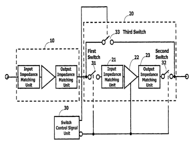
Figure 1 illustrates a related art multiple power mode power amplifier using
bypass switching circuits. The multiple power mode power amplifier illustrated
in
Figure 1 is configured using 3 bypass switching circuits. -
If the power amplifier is operated in the high power mode, both a first
switch 31 and a second switch 32 are closed and a third switch 33 is open, so
that
output of a driver 10 including an impedance matching unit is inputted into a
power
stage 22. In contrast, if the power amplifier is operated in the low power
mode,
both the first switch 31 and the second switch 32 are open and the third
switch 33 is
closed, so that output of the driver 10 including the impedance matching unit
bypasses the power stage 22.
Since the multiple power mode power amplifier illustrated in Figure 1 uses
3 bypass switching circuits, the degree of freedom in configuration of the
multiple
power mode power amplifier increases. However, at the same time, it has
disadvantages in that the size of the entire system increases and power loss
of the
entire system increases due to power loss of the bypass switching circuits.
Especially, power loss of the second switch 32 connected to an output terminal
of
the power stage affects efficiency and linearity of the operation in the high
power
mode a lot, so that a bypass switching circuit having great power capacity and
excellent loss characteristic should be used and the necessity of using the
bypass
switching circuit requires high cost.
Figure 2 illustrates a related art multiple power mode power amplifier using
other bypass switching circuits. The multiple power mode power amplifier
illustrated in Figure 2 is configured using not serial switches but shunt
switches.
In the high power mode, a shunt switch of a second bypass switching
3
CA 02514679 2005-07-27
WO 2004/062095 PCT/KR2003/000020
circuit 49 is connected to the ground and is operated with a third impedance
transformer 48 as an impedance matching unit. A first impedance transformer 47
transforms a load of an output stage including the second bypass switching
circuit
49 and the ~ third impedance transformer 48 into the optimum impedance Zopt
that
S makes an output of a power stage 45 maximum. A switch of a first bypass
switching circuit 44 is connected to an input terminal 43 of the power stage.
In the low power mode, the second bypass switching circuit 49 is
connected to an output terminal of a second impedance transformer and the
first
impedance transformer 47 forms an impedance matching unit together with the
second impedance transformer 46 and the third impedance transformer 48 by
transforming an output impedance of the power stage 45 which is off into
impedance of j50ohms. The switch of the first bypass switching circuit 44 is
connected to the input terminal of the second impedance transformer 46, so
that a
bypass is formed. The first bypass switching circuit 44 may be configured
using
two diode switches and the second bypass switching circuit 49 may be
configured
using one shunt diode switch.
Since the power amplifier illustrated in Figure 2 should use at least 3
switches, characteristic gets worse due to own losses of the switches and
price
competitiveness also gets worse due to an increase of the power amplifier's
size.
Figure 3a illustrates a related art multiple power mode power amplifier
using a bypass switching circuit, of which switching circuit is connected to
an
output terminal of ~,/4 bypass transmission line. The multiple power mode
power
amplifier illustrated in Figure 3a includes a carrier amplifier 51 and has a
bypass
implemented by a bypass switching circuit configured by using ~,/4 bypass
transmission line 52 and a shunt switch 53.
4
CA 02514679 2005-07-27
WO 2004/062095 PCT/KR2003/000020
In the high power mode, the shunt switch 53 of the bypass switching circuit
is connected to the ground and the bypass switching circuit including the
shunt
switch 53 is operated as an open stub by being connected to the 7~/4 bypass
transmission line 52.
In the low power mode, the shunt switch 53 of the bypass switching circuit
is connected to an output terminal of the carrier amplifier 51 and is operated
as an
bypass together with the ~,/4 bypass transmission line 52.
Figure 3b illustrates a related art multiple power mode power amplifier
using a bypass switching circuit, of which switching circuit is connected to
an input
terminal of ~,/4 bypass transmission line.
The difference between the multiple power mode power amplifier
illustrated in Figure 3b and the multiple power mode power amplifier
illustrated in
Figure 3a is only the order of a ~,/4 bypass transmission line and a bypass
switching
circuit.
Since the multiple power mode power amplifier illustrated in Figures 3a
and 3b includes only one bypass switching circuit, it has an advantage in that
the
size of the entire system is small. However, at the same time, it has an
disadvantage in that bandwidth is limited due to use of a ~,/4 bypass
transmission
line.
Figure 4 illustrates a related art multiple power mode power amplifier using
other bypass switching circuits.
Q3 (65) is a carrier amplifier and Q2 (62) is an operational amplifier. A
serial switch 66 comprises two parallel diodes and anodes of the diodes are
connected to Vcc of the carrier amplifier.
In the high power mode, Q1 (68) is off and the serial switch 66 is open.
5
CA 02514679 2005-07-27
WO 2004/062095 PCT/KR2003/000020
Accordingly, output of Q2 (62) is inputted into Q3 (65) and a first impedance
matching unit 63 is an impedance matching unit that transforms input impedance
into impedance of l5ohms.
In the low power mode, base bias of Q3 (65) is off and Ql (68) is on, so
that the switch 66 is closed. A second impedance matching unit 64 is an
impedance matching unit that transforms load impedance into impedance of
25ohms. The second impedance matching unit 64 has smaller impedance than
input impedance of Q3 (65) when the switch 66 is closed and has bigger
impedance
than input impedance of Q3 (65) when the switch 66 is open. Thus, the second
impedance matching unit 64 is operated as a bypass.
DISCLOSURE OF THE INVENTION
An object of the present invention is to solve at least the above problems of
the related art multiple power mode power amplifier using bypass switching
circuits
and to provide a multiple power mode power amplifier with high efficiency that
may amplify power of various levels without using bypass switching circuits by
making a path for bypassing a power stage and a path for passing through a
power
stage join at optimum point and implementing optimum impedance transformer on
the path for bypassing the power stage.
There is provided a multiple power mode power amplifier with high
efficiency including: a power stage for receiving power amplified by a driver
through a first impedance matching unit connected in serial to the driver
amplifying
input power and a second impedance matching unit connected to the first
impedance
matching unit in serial, re-amplifying the power and outputting the re-
amplified
6
CA 02514679 2005-07-27
WO 2004/062095 PCT/KR2003/000020
power; an applied voltage control circuit, connected to the power stage in
parallel,
for controlling applied voltages corresponding to a first power mode and a
second
power mode; an impedance transformer for receiving power amplified by the
driver
through the first impedance matching unit, according to operations of the
applied
voltage control circuit; a third impedance matching unit, connected to the
power
stage in serial, for receiving power amplified by the power stage, according
to
operations of the applied voltage control circuit; and a fourth impedance
matching
unit, connected to the third impedance matching unit in serial and connected
to the
impedance transformer in serial, for transferring power, transferred from the
third
impedance matching unit or the impedance transformer, to an output stage
according to operations of the applied voltage control circuit.
Preferably, the power stage is connected to the second impedance matching
unit in serial and, in the second power mode, the power stage receives power
amplified by the driver through the second impedance matching unit and re
amplifies the power.
Preferably, the applied voltage control circuit adjusts voltage applied to the
power stage in order for the power stage to be off in the first power mode and
in
order for the power stage to be on in the second power mode.
Preferably, the impedance transformer is connected in parallel to the
second impedance matching unit, the power stage and the third impedance
matching
unit and, in the first power mode, the impedance transformer receives through
the
first impedance matching unit the power amplified by the driver and outputs
the
power to the fourth impedance matching unit. Further, the impedance
transformer
has the structure of a band-pass filter.
Preferably, the third impedance matching unit prevents power transferred
7
CA 02514679 2005-07-27
WO 2004/062095 PCT/KR2003/000020
through the impedance transformer from leaking to the power stage.
Preferably, the fourth impedance matching unit receives power from the
impedance transformer in the first power mode and the fourth impedance
matching
unit receives power from the third impedance matching unit in the second power
mode.
Preferably, a path, that power which passed through the first impedance
matching unit is transferred to the fourth impedance matching unit, is
determined by
comparing impedance as viewed from the first impedance matching unit towards
the power stage and impedance as viewed from the first impedance matching unit
towards the impedance transformer.
Preferably, the impedance as viewed from the first impedance matching
unit towards the impedance transformer forms an inter-stage matching unit
between
the driver and the power stage together with the first impedance matching unit
in the
second power mode.
There is provided another multiple power mode power amplifier with high
efficiency including: a driver for variably amplifying gain of input signal
using a
variable gain amplifier; a power stage for receiving power amplified by the
driver
through a first impedance matching unit connected to the driver in serial and
a
second impedance matching unit connected to the first impedance matching unit
in
serial, re-amplifying the power and outputting the re-amplified power; an
applied
voltage control unit, connected to the power stage in parallel, for
controlling an
applied voltage corresponding to the first power mode and the second power
mode;
an impedance transformer for receiving through the first impedance matching
unit
power amplified by the driver according to operations of the applied voltage
control
circuit; a third impedance matching unit, connected to the power stage in
serial, for
8
CA 02514679 2005-07-27
WO 2004/062095 PCT/KR2003/000020
receiving power amplified by the power stage according to operations of the
applied
power control circuit; and a fourth impedance matching unit, connected to the
third
impedance matching unit in serial and connected to the impedance transformer
in
serial, for transferring the power transferred from the third impedance
matching unit
or the impedance transformer, to an output stage according to operations of
the
applied voltage control circuit.
Preferably, the power stage is connected to the second impedance matching
unit in serial and, in the second power mode, the power stage receives through
the
second impedance matching unit power amplified by the driver and re-amplifies
the
power.
Preferably, the applied voltage control circuit controls the driver in order
for gain of signal inputted into the driver to be differently amplified
corresponding
to the first power mode and the second power mode. The applied voltage control
circuit adjusts voltage applied to the power stage in order for the power
stage to be
off in the first power mode and in order for the power stage to be on in the
second
power mode.
Preferably, the impedance transformer is connected in parallel to the
second impedance matching unit, the power stage and the third impedance
matching
unit and, in the first power mode, the impedance transformer receives through
the
first impedance matching unit power amplified by the driver and outputs the
power
to the fourth impedance matching unit. The impedance transformer has the
structure of a band-pass filter.
Preferably, the third impedance matching unit prevents power transferred
through the impedance transformer from leaking to the power stage.
Preferably, the fourth impedance matching unit receives power from the
9
CA 02514679 2005-07-27
WO 2004/062095 PCT/KR2003/000020
impedance transformer in the first power mode and the fourth impedance
matching
unit receives power from the third impedance matching unit,
Preferably, a path, that power which passed through the first impedance
matching unit is transferred to the fourth impedance matching unit, is
determined by
comparing impedance as viewed from the f rst impedance matching unit towards
the power stage and impedance as viewed from the first impedance matching unit
towards the impedance transformer.
Preferably, the impedance as viewed from the first impedance matching
unit towards the impedance transformer forms an inter-stage matching unit
between
the driver and the power stage together with the first impedance matching unit
in the
second power mode.
BRIEF DESCRIPTION OF THE DRAWINGS
Figure 1 illustrates a related art multiple power mode power amplifier using
bypass switching circuits.
Figure 2 illustrates a related art multiple power mode power amplifier using
other bypass switching circuits.
Figure 3a illustrates a related art multiple power mode power amplifier
using a bypass switching circuit, of which switching circuit is connected to
an
output terminal of ~,/4 bypass transmission line.
Figure 3b illustrates a related art multiple power mode power amplifier
using a bypass switching circuit, of which switching circuit is connected to
an input
terminal of ~,/4 bypass transmission line.
Figure 4 illustrates a related art multiple power mode power amplifier using
CA 02514679 2005-07-27
WO 2004/062095 PCT/KR2003/000020
other bypass switching circuits.
Figure 5 illustrates a multiple power mode power amplifier with high
efficiency using power mode transition structure without a bypass switching
circuit
according to one preferred embodiment of the present invention.
Figure 6 illustrates the multiple power mode power amplifier with high
efficiency illustrated in Figure 5 in detail for explaining power mode
transition
structure without a bypass switching circuit.
Figure 7a is a graph illustrating gain characteristic corresponding to the
high power mode and the low power mode of the multiple power mode power
amplifier according to one preferred embodiment of the present invention.
Figure 7b is a graph illustrating Power Added Efficiency (PAE)
characteristic corresponding to the high power mode and the low power mode of
the
multiple power mode power amplifier according to one preferred embodiment of
the present invention.
Figure 8 illustrates a multiple power mode power amplifier with high
efficiency using power mode transition structure without a bypass switching
circuit
according to another preferred embodiment of the present invention.
BEST MODE FOR CARRYING OUT THE INVENTION
Hereinafter, a detailed explanation will be given with reference to the
attached drawings as to the multiple power mode power amplifier with high
efficiency in accordance with preferred embodiments of the present invention.
Hereinafter, the first power mode is called as the low power mode and the
second
power mode is called as the high power mode.
11
CA 02514679 2005-07-27
WO 2004/062095 PCT/KR2003/000020
Figure 5 illustrates a multiple power mode power amplifier with high
efficiency using power mode transition structure without a bypass switching
circuit
according to one preferred embodiment of the present invention.
The multiple power mode power amplifier with high efficiency illustrated
in Figure 5 includes: a driver 100 for amplifying input power; a power stage
120 for
receiving power amplified by the driver 100 through a first impedance matching
unit 130 connected in serial to the driver and a second impedance matching
unit 140
connected to the first impedance matching unit 130 in serial, re-amplifying
the
power and outputting the re-amplified power; an applied voltage control
circuit 90,
connected to the power stage 120 in parallel, for controlling applied voltages
corresponding to the low power mode and the high power mode; an impedance
transformer 170 for receiving power amplified by the driver 100 through the
first
impedance matching unit 130, according to operations of the applied voltage
control
circuit 90 and transferring the power to a fourth impedance matching unit 160;
a
third impedance matching unit 150, connected to the power stage 120 in serial,
for
transferring power amplified by the power stage 120 to the fourth impedance
matching unit 160; and the fourth impedance matching unit 160, connected to
the
third impedance matching unit 150 in serial and connected to the impedance
transformer 170 in serial, for transferring power, transferred from the third
impedance matching unit 150 or the impedance transformer 170, to an output
stage
78 according to operations of the applied voltage control circuit 90.
The applied voltage control circuit 90 adjusts voltage applied to the power
stage 120 by exterior control signal inputs corresponding to the low power
mode
and the high power mode. Since output power is gained by passing through not
the power stage 120 but, the optimized first impedance matching unit 130 and
the
12
CA 02514679 2005-07-27
WO 2004/062095 PCT/KR2003/000020
optimized impedance transformer 170, in the low power mode, the applied
voltage
control circuit 90 adjusts voltage applied to the power stage 120 in order for
transistors of the power stage 120 to be off.
In contrast, since output power is obtained by passing through the first
impedance matching unit 130, the second impedance matching unit 140 and the
power stage 120, the applied voltage control circuit 90 applies voltage
appropriate
for operations of transistors of the power stage 120.
The driver 100 in the low power mode amplifies input power and transfers
the amplified power to the impedance transformer I70 through the optimized
first
impedance matching unit 130. In contrast, the driver 100 in the high power
mode
amplifies input power and transfers the amplified power to the power stage 120
through the optimized first impedance matching unit 130 and the optimized
second
impedance matching unit 140.
The power stage 120 in the low power mode is off by the applied voltage
control circuit 90 and the power stage 120 in the high power mode amplifies
signal,
amplified by the driver 100 and inputted into the power stage 120.
The first impedance matching unit 130 is a circuit optimized for optimal
operations corresponding to the low power mode and the high power mode. The
first impedance matching unit 130 selectively transfers input power amplified
by the
driver 100 corresponding to operation modes to the impedance transformer 170
or
the power stage 120.
The second impedance matching unit 140 is a circuit optimized for optimal
operations corresponding to the low power mode and the high power mode. The
second impedance matching unit 140 transfers power, amplif ed by the driver
100
and transferred through the first impedance matching unit 130, to the
impedance
13
CA 02514679 2005-07-27
WO 2004/062095 PCT/KR2003/000020
transformer 170 in the low power mode and to the power stage 120 in the high
power mode.
The impedance transformer 170 is an impedance transforming circuit that
transforms impedance appropriately corresponding to the low power mode and the
high power mode. In the low power mode, the impedance transformer 170 forms a
path that bypasses the power stage 120, so that output of the driver 100 is
transferred to output stage 78 of the power amplifier.
Figure 6 illustrates the multiple power mode power amplifier with high
efficiency illustrated in Figure 5 in detail for explaining power mode
transition
structure without bypass switching circuit.
Output power of the driver 100 reaches a junction 72 dividing paths
corresponding to power modes via the first impedance matching unit 130.
In the low power mode, the power stage 120 is off by voltage applied by
the applied voltage control circuit 90 and input impedance Z rrrT-H Of the
power
1 S stage 120 as viewed from the first impedance matching unit 130 is quite
larger than
input impedance Z irrT-z of a path bypassing the power stage 120 as viewed
from the
first impedance matching unit 130. Thus, power amplified by the driver 100 and
transferred to the junction 72 is optimized so that the amount of power
inputted into
the impedance transformer 170 is quite larger than the amount of power
inputted
into the power stage 120. The output power is transferred to the output stage
78
with minimizing power leakage to the power stage by the third impedance
matching
unit 150 and the fourth impedance matching unit 160.
In the high power mode, the power stage 120 is on by voltage applied by
the applied voltage control circuit 90 and input impedance Z nrT-H Of the
power
stage 120 as viewed from the first impedance matching unit 130 is smaller than
14
CA 02514679 2005-07-27
WO 2004/062095 PCT/KR2003/000020
input impedance Z ~T-L Of a path bypassing the power stage 120 as viewed from
the
first impedance matching unit 130. Thus, most power, amplified by the driver
100
and transferred to the junction 72, is amplified by the power stage 120 and is
transferred to the output stage 78 of the power amplifier with minimizing
power
leakage to the impedance transformer 170 by the optimized third impedance
matching unit 150 and the optimized fourth impedance matching unit 160.
Input impedance Z ~T-L Of a path bypassing the power stage 120 as viewed
from the first impedance matching unit 130 forms an inter-stage matching unit
between the driver 100 and the power stage 120 together with the first
impedance
matching unit 130 in the high power mode, so that output power of the driver
I00 is
well transferred to the power stage 120.
Figure 7a is a graph illustrating gain characteristic corresponding to the
high power mode and the low power mode of the multiple power mode power
amplifier according to one preferred embodiment of the present invention.
In the low power mode, the power stage 120 is off by the applied voltage
control circuit 90, so that output of the driver 100 is not amplified by the
power
stage 120 and the output of the driver 100 is transferred to the output stage
78
through the impedance transformer 170. Thus, it is impossible to get such gain
characteristic at the time of being amplified by the power stage 120. However,
DC
power consumption by the power stage 120 can be removed, so that PAE
characteristic is excellent.
In contrast, output of the driver 100 is amplified by the power stage 120
and reaches the output stage 78, in the high power mode, so that the gain
characteristic at the time of being amplified by the power stage 120 is added
to the
gain characteristic by the operation in the low power mode and PAE
characteristic
CA 02514679 2005-07-27
WO 2004/062095 PCT/KR2003/000020
depends on the power stage 120 having generally high output power level.
Accordingly, as illustrated in Figure 7a, gain characteristic is comparatively
low in the low power mode and gain characteristic is comparatively high in the
high
power mode.
Figure 7b is a graph illustrating Power Added Efficiency characteristic
corresponding to the high power mode and the low power mode of the multiple
power mode power amplifier according to one preferred embodiment of the
present
invention.
As illustrated in Figure 7a, PAE characteristic in the low power mode is
excellent because DC power consumption by the power stage 120 can be removed.
In the high power mode, output of the power stage 120 is transferred to the
output
stage 78 through the third impedance matching unit 150 and the fourth
impedance
matching unit 160, and the third impedance matching unit 150, the fourth
impedance matching unit 160 and the impedance transformer 170 do not use a
switch, so that output of the power stage 120 is transferred to the output
stage 78
without loss and thus PAE characteristic in the high power mode is excellent.
Figure 8 illustrates a multiple power mode power amplifier with high
efficiency using power mode transition structure without a bypass switching
circuit
according to another preferred embodiment of the present invention.
The multiple power mode power amplifier with high efficiency using
power mode transition structure without a bypass switching circuit according
to
another preferred embodiment of the present invention comprises: a driver 210
for
variably amplifying gain of input signal using a variable gain amplifier; a
power
stage 220 for receiving power amplified by the driver 210 through a first
impedance
matching unit 230 connected to the driver 210 in serial and a second impedance
16
CA 02514679 2005-07-27
WO 2004/062095 PCT/KR2003/000020
matching unit 240 connected to the first impedance matching unit 230 in
serial, re-
amplifying the power and outputting the re-amplified power; an applied voltage
control unit 190, connected to the power stage 220 in parallel, for
controlling an
applied voltage corresponding to the low power mode and the high power mode;
an
impedance transformer 270 for receiving through the first impedance matching
unit
230 power amplified by the driver 210 according to operations of the applied
voltage control circuit 190; a third impedance matching unit 250, connected to
the
power stage 220 in serial, for receiving power amplified by the power stage
220
according to operations of the applied power control circuit; and a fourth
impedance
matching unit 260, connected to the third impedance matching unit 250 in
serial and
connected to the impedance transformer 270 in serial, for transferring the
power
transferred from the third impedance matching unit 250 or the impedance
transformer 270, to an output stage 178 according to operations of the applied
voltage control circuit.
The applied voltage control circuit 190 controls the driver in order for gain
of signal inputted into the driver to be differently amplified corresponding
to the
low power mode and the high power mode. The applied voltage control circuit
adjusts voltage supplied to the power stage 220 by exterior control signal
inputs
corresponding to the low power mode and the high power mode. Since output
power is gained by passing through not the power stage 220 but, the optimized
first
impedance matching unit 230 and the optimized impedance transformer 270, in
the
low power mode, the applied voltage control circuit 190 adjusts voltage
applied to
the power stage 220 in order for transistors of the power stage 220 to be off.
In contrast, since output power is obtained by passing through the first
impedance matching unit 230, the second impedance matching unit 240 and the
17
CA 02514679 2005-07-27
WO 2004/062095 PCT/KR2003/000020
power stage 220, the applied voltage control circuit 190 applies voltage
appropriate
for operations of transistors of the power stage 220.
The variable gain amplifier variably amplifies gain of signal inputted
through an input terminal 180 of the power amplifier according to operations
of the
applied voltage control circuit 190 and supplies the amplified gain to the
first
impedance matching unit 230, the power stage 220 and the impedance transformer
270. The variable gain amplifier performs a role of not only a driver but also
a
linearizer, so that efficiency and linearity of circuit can be optimized.
Further,
discontinuous gain characteristic of the power amplifier illustrated in Figure
7a can
be adjusted corresponding to use.
The power stage 220 in the low power mode is off by the applied voltage
control circuit 190 and the power stage 220 in the high power mode amplifies
signal, amplified by the driver 210 and inputted into the power stage 220.
The first impedance matching unit 230 is a circuit optimized for optimal
operations corresponding to the low power mode and the high power mode. The
first impedance matching unit 230 selectively transfers input power amplified
by the
driver 210 corresponding to operation modes to the impedance transformer 270
or
the power stage 220.
The second impedance matching unit 240 is a circuit optimized for optimal
operations corresponding to the low power mode and the high power mode. The
second impedance matching unit 240 transfers power, amplified by the variable
gain
amplifier and transferred through the first impedance matching unit 230, to
the
impedance transformer 270 in the low power mode and to the power stage 220 in
the high power mode. '
The impedance transformer 270 is an impedance transforming circuit that
18
CA 02514679 2005-07-27
WO 2004/062095 PCT/KR2003/000020
transforms impedance appropriately corresponding to the low power mode and the
high power mode, In the low power mode, the impedance transformer 270 forms a
path that bypasses the power stage 220, so that output of the driver 210 is
transferred to output stage 17~ of power amplifier.
The multiple power mode power amplifier according to the present
invention is not limited to the preferred embodiments and may be implemented
without departing from the scope and spirit of the invention as disclosed in
the
accompanying claims by various modification by those skilled in the art.
INDUSTRIAL APPLICABILITY
The multiple power mode power amplifier according to the present
invention amplifies power of various levels without using a bypass switching
circuit, so that problems in that losses caused by using bypass switching
circuits in a
related art multiple power mode power amplifier, an increase of the size of
the
power amplifier, price competitiveness deterioration and etc. can be solved.
Further, the multiple power mode power amplifier according to the present
invention reduces l~C power consumption in the low power mode practically
affecting battery lifetime, so that PAE characteristic of the power amplifier
may be
improved and talk time of a mobile handset equipped with the multiple power
mode
power amplifier according to the present invention may be extended.
Further, the present invention that adopts a variable gain amplifier as a
driver minimizes losses of the related art multiple power mode power amplifier
in
the high power mode, so that PAE characteristic in the high power mode may be
improved and bad linearity in the high power mode may be solved. Further,
19
CA 02514679 2005-07-27
WO 2004/062095 PCT/KR2003/000020
improvement of speech quality of a mobile handset equipped with the multiple
power mode power amplifier according to the present invention and reduction of
the
size of the mobile handset equipped with the multiple power mode power
amplifier
according to the present invention may be implemented.