Note: Descriptions are shown in the official language in which they were submitted.
CA 02522396 2005-10-07
WO 2004/097783 PCT/US2004/012122
Description
LED ILLUMINATION SOURCE/DISPLAY WITH INDIVIDUAL LED BRIGHTNESS
MONITORING CAPABILITY AND CALIBRATION METHOD
RELATED APPLICATION
This application is based on U.S. Provisional Application Serial No.
60/465,437, filed
April 25, 2003, entitled Self Calibrating Video Display Apparatus and claims
the benefit of the
filing date thereof,for all common subject matter.
FIELD OF THE INVENTION
This invention relates to an LED illumination source/display particularly
suitable for
large format video and graphic displays in the form of signs and billboards
suitable for viewing
by a large number of individuals.
BACKGROUND OF THE INVENTION
Prior Art Video Displa,~s
Large signs and billboards have been in wide use for many years as a medium
for
advertising and for imparting information to the public. Traditionally, signs
and billboards
have been used to exhibit a single advertising theme, product or message. Due
to the fixed
print nature of this medium, it does not Lend itself to displaying a larger
series of ideas as would
be common with a medium such as television. Phosphor and incandescent emissive
based
display technologies have to a limited extent achieved success in displaying
varying images in
Large outdoor and indoor displays. However, advances of technology in
illumination sources
such as light emitting diodes (LEDs) have allowed such diodes to largely
replace phosphor and
incandescent displays for large format outdoor and indoor displays, e.g.,
having a diagonal
dimension in excess of 100 inches, which are to be viewed from distances of 20
or more feet in
ambient lighting conditions requiring display brightness of say over 500 nit.
The term LED is
used herein to collectively refer to the light generating semiconductor
element, i.e., LED DIE as
well as the element packaged with a lens and/or reflector.
The current economics and price/performance of traditional LED video and
graphic
displays is sufficient to replace incandescent, CRT and protection display
technology in the
existing high value markets, however, the traditional LED displays themselves
have drawbacks
CA 02522396 2005-10-07
WO 2004/097783 PCT/US2004/012122
2
that impair the growth potential of such displays.
LED video/graphic boards, as they are common called, utilize color LEDs
arranged in
pixels (as discrete groups) forming an array. Each pixel, which comprises a
group of LEDs,
e.g., red (R), blue (B), and green (G), is capable of emitting light of a
desired color or hue
representing the smallest increment (or perceived point) of the displayed
image.
LED Displays and the De rg adation Problem
The benefits of brightness, life and power saving of LEDs, used as
illumination sources,
come with a random distribution of brightness, dominant wavelength (color
coordinate), and
LED chip (DIE) structure with its inherent degradation during use at the pixel
level. The
degradation rates and profiles are different fox individual LEDs or packaged
LEDs within a
production run or lot. Sorting the individual LEDs into smaller distributions
of brightness and
hue-bounded ranges, reduces the negative effect on initial quality only. The
long term effect of
LED degradation results from LED accumulated operational time and is
accelerated by
increases in operating junction current, temperature and humidity. The
degradation profile also
varies by the uniformity of the LED junction resulting in the intuitive and
empirical deduction
that brighter LEDs (or packaged LEDs) and therefore LEDs from a particular
wafer lot are also
structurally better LEDs with lower degradation rates than the lower
brightness LEDs from the
same lot.
The operating time of video display and advertising systems used for sporting
events
averages less than 800 hours per year. Such a system would rarely be in
operation over 1,500
hours a year even in a common area accommodating two sporting events such as
basketball and
hockey. In such use the accumulated individual pixel energization or per
primary color LED(s)
in a dual use would be less than 400 hours for blue and near 800 for red and
somewhat less for
green.
Out of home advertising ("OHA") is generally calculated to place about an
8,760 hour
per year burden on the display system. In addition, such advertising is
dominated by static
image content that results in an increased operational time over the video
intensive content of
sporting events. High ambient light OHA locations may result in content and
LED lamp
operational time estimated to be well over 20,000 hours in a five year period.
Other variables,
such as border vs. center module distribution, dominant color of image and
background may
exacerbate a pixel or group of pixel's operational time and thereby the
degradation of the LEDs
CA 02522396 2005-10-07
WO 2004/097783 PCT/US2004/012122
constituting a pixel or group of pixels.
OHA is dominated by still images where the quality benchmark is print media
and
image quality is often critical. According to Mr. Charles Poynton, a
recognized authority on
color in electronic displays, a color difference > 1 % is discernable to an
average observer.
Advertising content for food, clothing, cosmetics and automobiles often
contain fine shading
and gradual color gradients. Accurate color rendering is essential to image
quality and
ultimately advertiser satisfaction and consumer acceptance of an accurate
rendering of the
actual merchandise.
In our prior U.S. Patent No. 6,657,605 ("'605 patent"), the LED modules making
up the
display are characterized at the pixel level to make uniformity correction
possible. Uniformity
correction, in turn, provides a uniform brightness of each primary color LED
within the entire
display.
Uniformity correction with external light sensors is discussed generally in
the '605
patent and is recapped below:
LED lamps from Nichia or other vendors such as Agilent, Lite-On, Kingbright,
Toyoda
Gosei and others, are sorted into groups called ranks or bins having an
intensity variance of
candlepower (cd.) +/- 15% to +/- 20%. The implementation of uniformity
correction begins
with the assumption that like ranks of LED lamps having a +/- 10% variance may
be procured
from the above suppliers at a modest premium. Volume production of the video
display
apparatus referred to as LED modules then takes place with specific ranks used
in specific LED
modules. In LED modules so constructed, the LEDs of one rank are operated at
one forward
current level Ifr, determined by their ranlc and LEDs in other LED modules of
lower rank are
operated at a higher level, such that all LED modules used in a particular
display during a
production lot, have a similar non-uniformity corrected average brightness
that approximates
D6500 white (i.e., simulation of the radiation from a black body at
6500°k) when operated at
the same R, G, B level.
In accordance with this preferred method, the power supply and constant
current source
drive electronics for energizing the LEDs varies the LED(s) output intensity
by modulating a
fraction or percentage of the time the LED(s) is turned on within an image
frame interval. Such
modulation is commonly referred to as pulse width modulation (PWM). The term %
ON TIME
as used herein denotes that percentage value which may vary between 0 and 100,
where 0
CA 02522396 2005-10-07
WO 2004/097783 PCT/US2004/012122
4
represents the LED is fully off and 100 represents that the LED is fully on.
Next a characterization or test system measures the brightness of each LED
color in
each pixel of the module when operated at a fixed levels) of input energy to a
high level of
repeatability (<+/-2%). The normalized brightness of R, G, and B color
required for SMPTE
D6500 white for the whole display configured of specific LED modules is then
calculated and a
table of uniformity correction coefficients generated. The system applies the
uniformity
correction coefficient data to the image data which causes each pixel to
perform as if it were
part of a matrix of LED pixels having uniform intensity.
Prior Art Approaches to the Degradation Problem
The LED display, so comprised, will appear to have an image quality noticeably
superior to those that do not employ some form of uniformity correction. While
this solution
provides for exceptional image quality of a new display, the long-term
prognosis leaves much
to be desired outside the intermittent operation during sporting events. As an
LED display ages
the maintenance cost escalates and average color uniformity degrades in a
somewhat predictive
manner determined by LED accumulated operational time. Some LED video display
manufacturers use a predictive algorithm to compensate for LED degradation
within the
display. Non-predictive factors such as environmental stress in packaging and
individual DIE
characteristics cannot be accounted for based on content derived predictive
models. This
deficiency may be overcome by measuring the brightness, i.e., luminous
intensity, of each color
LED(s) within each pixel and compensating for the degradation by supplying
additional energy
or % ON-TIME in response to the signal image data for that pixel such that it
produces the
same optical output as it did when the pixel's output was first characterized.
The industry standard LED display module construction employs an array of
"Super-
oval" 50 deg x 110 deg, LED lamps soldered to a printed circuit board which is
then affixed to
and potted within a mounting frame where the potting material sealing the LED
lamps is black
opaque to provide contrast to the emitted image Light. A typical 13'4" x 48'
electronic bulletin
billboard will have 92,160 pixels spaced 1" apart and 368,640 LEDs contained
within its 360,
16 pixel x 16 pixel, LED modules.
Once the display is placed in the field the only practical way to counteract
LED
degradation is to use an external measurement device such as an externally
positioned
calibrated CCD camera to measure the value of the light output of each LED
within each pixel.
CA 02522396 2005-10-07
WO 2004/097783 PCT/US2004/012122
This value can then be compared to the value at the time of characterization
and the
energization of each LED can then be adjusted to achieve a uniform response to
a known
generated pattern. While this method may be suitable for displays concentrated
in locations
such as Las Vegas, Times Square, and the Los Angeles Sunset Strip, it is not
feasible to
maintain the calibration of the image quality of thousands of electronic
billboards that would be
fielded by the billboard operators in the United States.
There is clearly a need for an LED illumination source such as an LED
billboard
module design that is able to maintain the display's image quality without the
use of an external
measurement device. In particular, there is a need for a feedback based light
sensor that is
internal to the illumination source/display which can provide a measure of the
light emitted,
e.g., luminous intensity representative of a discrete color, from each LED(s)
within each pixel.
The term pixel as used herein means a group of LEDs which represent a finite
area of the
source or the smallest increment or perceived point on a display and capable
of replicating all of
the colors and hues of the source/display.
With respect to the use of light sensors with LEDs it is not new to package
such a
sensor/detector together with an LED. For example, opto-isolator or opto-
couplers have been
widely used for the purpose of transmitting data across an electrically
isolating barrier through
an optically transmissive medium such as a light pipe. Photodiodes are also
used to provide
feedback as an integral part of a laser diode package for output control.
Also see U.S. Patent No. 5,926,411 issued to James T. Russell which describes
a CCD
detector and circuit to set the threshold for data detection and even the
possibility of using the
LED as a detector. Notwithstanding the existence of LED sign and billboard
display systems
and the specialized prior art use of photodetectors the need discussed above
has remained
unfulfilled.
Objects of the Invention
An objective of the present invention is to provide a means for an LED display
to detect
and compensate for expected degradation of the LEDs' light output over the
life of the display.
It is a further object to provide an integral photodetector in close proximity
with one or more
LEDs to enable the light output from each LED(s) at any time during its life
to be measured. It
is another object to produce and maintain a quality image on an LED display
composed of a
multitude of pixels by controlling the absolute output luminance of every LED
representative of
CA 02522396 2005-10-07
WO 2004/097783 PCT/US2004/012122
6
each discrete color in each pixel so that the display appears uniform in
brightness and color
across the entire display.
The term "LED(s)" as used herein means the single or multiple LEDs in each
pixel
which are responsible for emitting light of a discrete color. For example, two
red LEDs are
illustrated in Fig. 4 for emitting light perceived as red.
SUMMARY OF THE INVENTION
An LED area illumination source or display, such as an electronic billboard
display, is
made up of a plurality of individual pixels of LEDs with each pixel comprising
a plurality of
LEDs, e.g., red, green and blue packaged singly or together, with the LED(s)
representing a
discrete color being arranged to be separately energized so that by
simultaneously energizing
one or more of the LEDs any desired color can be emitted from the pixel. At
least one light
sensor is arranged to provide an output signal representative of a measure,
e.g., the luminous
intensity of emitted light from each of the LED(s) of the source/display when
said LED(s) is
separately energized. At least one light sensor may comprise a sensor
associated with one or
more pixels or with each LED.
In accordance with a method of determining the LED degradation in the
source/display,
each LED(s) representing a discrete color in each pixel is separately
energized at a given level
which may, but need not be, the same for all LEDs, e.g., 100% ON TIME, at a
time to of
characterization. At the same time the output signal of the associated light
sensor is read and
stored with the output signal bearing a given relationship with the emitted
light, e.g., luminous
intensity and the level of energization. At a time t~ subsequent to to each
LED(s) representing a
discrete color of each pixel is separately energized at a given level, e.g.,
100% ON TIME and
the output signal of the associated sensor is read and compared with a value
of the
corresponding output signal at to.
Assuming that the display, at the time of characterization is operated at less
than the
maximum energy level for all LEDs, e.g., less than 100% ON TIME, the
individual LEDs may
be restored to their characterization status, by using the difference between
the to and t" sensor
output signals to control, i.e., increase, the energization, e.g., % ON TIME
of each LED(s)
which has suffered degradation.
The construction and operation of the present invention may best be understood
by
reference to the following description taken in conjunction with the appended
drawings.
CA 02522396 2005-10-07
WO 2004/097783 PCT/US2004/012122
BRIEF DESCRIPTION OF THE DRAWINGS
Fig. 1 is a front view of a video display module comprised of an array of
pixels with
each pixel including a plurality of LEDs;
Fig. 2 is a block diagram of an electronic system for supplying energy to the
LEDs in
the array of fig. 1 and reading the outputs of the embedded photodetectors;
Fig. 3 is a front view of one of the pixels of Fig. l;
Fig. 4 is a cross-sectional view taken along line 4-4 of Fig. 3;
Figs. 5, 6, and 7 are perspective, top plan (with the lens omitted), and cross-
sectional
views, respectively, of an alternative pixel arrangement in which Led active
elements, i.e., LED
DIEs are packaged together with the active element of a photodiode in a single
envelope;
Fig. 6a is a blown-up plan view of the LED/photodiode active element of Fig.
6;
Figs. 8, 9 and 10 are perspective, top plan, and cross-sectional side views,
respectively,
of a modified embodiment of the pixel of Figs. 5-7;
Fig. 11 is a cross-sectional view of a pixel being calibrated or characterized
by a
spectraradiometer;
Fig. 12 is a block diagram of a test system for characterizing the display
module;
Fig. 13 is a diagrammatic view of a section of the photodetector array of Fig.
2 along
with a measurement circuit for reading the detector outputs;
Fig. 14 is a flow chart of an algorithm for self calibrating a single LED;
Fig. 15 is a more detailed flow chart of the characterization algorithm and
correlation of
the photodetector outputs to the LED light output and energization level;
Fig. 16 is a flow chart illustrating optional operations of the display;
Fig. 17 is a flow chart showing the self calibration process; and
Figs. 18-21 are flow charts illustrating optional display modes.
DESCRIPTION OF THE PREFERRED EMBODIMENT
Use of an Internal Photodetector to Measure the Emitted and Ambient Light
An LED illumination source or display made up of an array of modules with each
module comprising individual LED groups or pixels, with each pixel
constituting a finite area
or smallest increment of the source or display, is described in our co-pending
U.S. application
serial number 10/705,515 ("'515 application"), filed November 16, 2003,
entitled Video
Display Apparatus and the '605 patent. The contents of the '515 application
and the '605
CA 02522396 2005-10-07
WO 2004/097783 PCT/US2004/012122
8
patent are incorporated herein by reference.
Referring now to the figures, Fig. I illustrates the LED video display module
or array I O
as described in the '60S patent in which the array is comprised of individual
pixels (picture
elements) 11. It is to be understood that a video display is conveniently
constructed of
individual modules which are assembled in an array to make up the completed
sign or
S billboard. The term "array" as used herein shall mean an individual module
or array. A system
for operating the array 10, while providing self calibration, is illustrated
in Fig. 2 in which
PWM current is supplied to the LED array via an electronic module 12
incorporated into the
array with the module I2, including a microcontroller 12a, a program memory
12b, a shared
memory 12c, a logic controller/power supply 12d and an analog processing
circuitry I2e. A PC
I O I4 controls the operation of the electronic module. A photodetector array
16, embedded in the
array, supplies the output signals from the individual light sensors or
photodetectors associated
with each pixel or LED to the electronic module 12 as will be explained.
The implementation of the illumination source/display 10 of the 'S 1 S
application, to
incorporate an internal Iight sensor/photodetector for measuring the emitted
light from each
1 S LED(s) representing a discrete or primary color and the electronics to
operate the same, is the
subject of this application. Only a single LED group or pixel will be
described in conjunction
with Figs. 4-10 with the understanding that many such pixels will be grouped
to form an array.
In addition, while the 'S 1 S application specifically provides for the use of
a diffractive optical
element to disperse the emitted light in an elliptical pattern, the present
invention is not limited
20 to the use of such a diffuser. Also, as will be discussed in more detail,
one or more LED DIEs
along with a light sensor can be mounted within a single optical package,
e.g., sharing a single
reflector/lens.
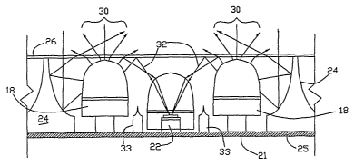
Figs. 3 and 4 illustrate a single pixel including two red LEDs 18, one blue
LED 19, and
one green LED 20. It is to be noted that the number of LEDs and the
distribution of color
2S within each pixel is not restricted to those just mentioned. To create
various color temperatures
additional LEDs with differing emitted wavelengths may be incorporated into a
pixel. The
LEDs are mounted on a printed circuit board 2I via a conventional surface or
through hole
mounting arrangement. A light sensor or photodetector 22 in the form, for
example, of a PIN
or PN photodiode is also mounted on the circuit board adjacent to the LEDs,
such as in a center
30 position, as shown in Fig. 3, to receive light emitted from each of the
LEDs. A housing 24
CA 02522396 2005-10-07
WO 2004/097783 PCT/US2004/012122
9
supports the circuit board and a light shaping diffuser 26, such as that
described in the '515
application, is adhesively bonded to the housing. Light, designated at 30, is
radiated out of the
pixel. Some of the light 32, emitted by each LED, is reflected internally, for
example, by the
diffuser 26 and reflectors 33 secured to the circuit board, such that a small,
but fixed percentage
of radiated pixel light is received by the photodiode 22 contained within the
pixel.
In an alternative embodiment to that shown in Figs. 3 and 4 the pixel may be
formed of
a chip set 34 in which a plurality of LED DIEs and a light sensor/photodiode
junction are
mounted on a common substrate as is illustrated in Figs. 6 and 7. The chip set
includes two red
LED DIES 36, one blue LED DIE 38, one green LED DIE 40 and a photodiode
junction 42.
The term light sensor/photodiode as used herein shall collectively refer to a
photodiode
packaged in a separate envelope as is illustrated in Figs. 3 and 4 or to the
junction packaged in
an envelope containing one or more LED DIES.
A one piece molded lens/reflector 44b is mounted to the circuit board 21 over
the chip
set 34. The lens/reflector is shown as including support posts 44a secured to
the underlying
circuit board.
Figs. 8-10 illustrate a fiuther embodiment to that shoran in Figs. 5-7 in
which the chip
set 34 is positioned within a reflector 46 which directs the light emitted
from the LEDs
outwardly in a somewhat collimated beam. In either of the above embodiments,
like the system
of Figs. 3 and 4, a poition of the LED emitted light is received by the
associated photodiode.
All the optical elements 18 - 20 and 22 of Figs. 3 and 4 or elements 36, 38,
40 and 42 of
Figs. 5-10 are fixed relative to each other as well as to the diffuser 26 and
the reflector 33 if
used. The amount of radiation impinging on the photodiode from any LED or
combination of
LEDs, representing a discrete color, e.g., red, within the pixel is in direct
linear proportion to
the radiation emitted by that LED or combination of LEDs within the pixel.
This assumes any
ambient light effect is eliminated or known and cancelled and that while the
responsivity of the
photodiode may vary for the red, blue and green LED spectral emission, the
response with
respect to any LED(s) remains constant over time and operating temperature.
This arrangement
of LEDs and internal photodiodes in an area illumination source or video
display allows for (1)
compensation of individual LED degradation (i.e., self calibration); (2)
detection of LED
catastrophic failure; (3) confirmation of the display image (i.e., content
validation); (4)
continuous display brightness (i.e., automatic brightness control) by
measurement of ambient
CA 02522396 2005-10-07
WO 2004/097783 PCT/US2004/012122
light level; (5) brightness compensation for a partially shadowed display and
(6) detection of a
light output obstruction (e.g., graffiti) as will be explained in more detail.
Overview of the Characterization of the Array and Preparation for Subsequent
Self
calibration
In order to display a quality image the brightness, i.e., luminance, i.e.,
luminous
5 intensity, and color i.e., chromaticity, of each pixel must be controlled by
modulating the
intensity of the individual LEDs in proportion to one another such that their
combined light
outputs produce the desired intensity and color. As pointed out earlier, in
the preferred
embodiment the display electronics of Fig. 2 varies an LED's light output
intensity by
modulating the fraction of time the LED is turned on within an image frame
interval, i.e. PWM.
10 This allows varying the LEDs perceived output intensity, i.e., luminance,
without changing its
perceived color.
In an overview of factory calibration, i.e., characterization, and subsequent
self
calibration, a test system shown in Figs 1 l and 12 sequentially drives each
LED (illustrated as
red LEDs in Fig. 11) at full output intensity, i.e., 100% ON TIME. The test
system includes a
PC 48 which controls an x-y table 54 on which the array is mounted during
characterization so
that each pixel is sequentially positioned under a calibrated
spectraradiometer 50 with its light
integrating sphere SOa (discussed in the '605 patent). The spectraradiometer
50 measures the
luminous intensity and spectral characteristics of each LED representative of
a discrete color in
each pixel. The test system computes a tri-stimulus value chromaticity vector
bxyn, for each
Led(s) representative of a discrete color corresponding to the CIE (Commission
Internationale
de 1'clairage) 2 deg xyz chromaticity coordinates for each primary color as
will be explained in
more detail in connection with Fig. 15. The measurement is stored in a file
which is then
transferred to and stored by the PC 14 of Fig. 2 for operational use.
The outputs of the embedded photodiodes 22 associated with each LED(s)
representative of a discrete color of each pixel are also measured with the
LED on and with the
LED off. Preferably the on measurement is made with the LED ON TIME set at
100%, as
pointed our earlier. The measured photodiode outputs are sometimes referred to
herein as
output signals. The off measurement, corresponding to the ambient light level,
is subtracted
from the on measurement corresponding to a.portion of the LED light output
plus the ambient
light level yielding a baseline photodetector measurement (Mo, Fig. 14) for
each LED(s)
CA 02522396 2005-10-07
WO 2004/097783 PCT/US2004/012122
11
representing a discrete colox for each pixel. This measurement is stored in
memory 12b for
operational use. A factor representative of the characteristic response,
(e.g., gain in terms of
Iumenslvolts) of each photodiode to the luminous intensity of the light from
each associated
LED(s) representing a discrete color within that pixel is also calculated and
stored in memory
12d at the time of characterization.
A factory calibration algorithm computes an initial, unique % ON TIME for each
LED(s) representing a discrete color for each pixel based on the following
criteria. The
luminous intensities for red, green, and blue LEDs are adjusted to be in
proportion to one
another such that the required white point, e.g., D6500 is achieved across the
entire display
when the display is commanded to display white. Further, the target White
Point luminance
output value is adjusted to be the same for each pixel so that uniform
brightness is achieved
across the entire display when all pixels are commanded to display the same
color and intensity.
Finally, it is noted that the selection of suitable LEDs with sufficient light
output assures that at
factory calibration sufficient intensity margin, i.e., head room, is provided
for such that as an
LED degrades in output intensity over time, its optical output intensity can
be increased to its
initial value by increasing the PWM(n) % ON TIME thereby maintaining uniform
intensity and
color balance across the entire display.
The final values of the energization level, i.e., % ON TIME for each LED(s)
representing a discrete color in each pixel (or group) is stored at the time
of characterization,
i.e., ta.
There are several circuits that may be utilized to read the output signals
from
photodiodes during characterization as well as subsequent calibration. One
such circuit
incorporates a light-to-frequency converter and a photodiode into a single
package or
component such as those manufactured by Taos, Inc. of Dallas, Texas. The light-
to-frequency
converter is a single integrated circuit with a photodiode sense array analog
detection circuit
and a digital output whose frequency is proportional to the LED luminous
intensity output from
the component.
The light-to-frequency converter component provides linearity over a broad
range of
light input signal and interfaces directly with digital microprocessors and
programmable logic
arrays. The downside to the use of such a anticipated component is cost in
view of the number
of devices required for a large array of pixels.
CA 02522396 2005-10-07
WO 2004/097783 PCT/US2004/012122
12
Another technique for measuring the light impinging on the photodiodes is
commonly
used in digital cameras. A circuit following this technique is shown in Fig.
13. The circuit
connects the photodiodes 22 in a conventional matrix along rows 52a
(illustrated as DRl-DRN
and columns 52b (illustrated as DC1-DCN). For sake of simplicity, voltage
(electron) sources
labeled VSM1 - VSMN, are connected to the cathodes of the rows of diodes as
shown. The
election sources, while shown separately, form part of a power electronics
module 12
incorporated in the LED display array.
A capacitor 56 is discharged through a discharge resistor 58 by a switching
transistor
60. The red, green or blue LED source in the pixel (row 1, column 1) to be
characterized or
calibrated is driven at a desired operating current level, e.g., 100% ON TIME
via PWM
electronic module 12. After the rise time of the drive circuit current has
expired the drive
current referred to as forward current will be stable, causing photons of the
specific color to be
radiated in proportion to the forward current for that specific LED(s) of the
individual pixel.
The electron source VSM1, via the module 12, supplies electrons to the
photodiode
row. At the same time transistor 60 is turned off removing the charge drain on
capacitor 56 and
transistor 62 is turned on allowing the measurement capacitor 56 for column 1
to begin to
accumulate a charge through a photodiode 22. The rate of charge is in direct
proportion to the
number of photons absorbed by the photodiode semiconductor element.
The electronics module 12, under the control of PC 14, measures time interval
Tm
between the column measurement capacitor 56 transitioning from 10% to 90% of
the source
voltage VSM1. Since the photodiode semiconductor element exchanges one
electron for one
photon absorbed, the portion of light absorbed by the photodiode from the LED
source is
thereby measured and supplied via an A/D converter labeled as 64 (incorporated
into 12e) to
the electronics module 12 for storage.
Any decrease in light output from the LED source of a particular pixel will
result in a
decrease in light measured by the PN or PIN-photodiode semiconductor element
and its
associated circuit within that particular pixel in direct proportion to the
amount of decrease.
Since the objective of the measurement is to determine the amount of LED
output
degradation it is only necessary to determine the percentage of decrease in
output relative to the
known output for the pixel at the time the characterization was made.
Alternatively, the
amount of increased input energy to the pixel LED required to bring the pixel
output to the
CA 02522396 2005-10-07
WO 2004/097783 PCT/US2004/012122
13
original level at characterization may be determined. It is therefore required
that the
measurement be accurate in the proportion of electrons exchanged for a light
level with the
pixel.
A new uniformity correction factor may then be calculated for red, green and
blue LED
output for each pixel that increases the amount of % ON TIME required to raise
the pixel
output for each color to the Level when that pixel was initially
characterized.
The amount of additional energy output required in the form of an increased %
ON
TIME needed to compensate for the LED degradation is calculated in the LED
module's
microprocessor and added to that required to generate a specific % ON TIME
energy output for
the image as determined by the display system logic producing uniformity
corrected data
delivered to the display modules.
Overview of Self calibration
The flow chart of a simplif ed self calibration algorithm is shown in Fig. 14.
At time to
the display is characterized as shown in step 64. At a later time 66 the
module determines if it
is time to re-calibrate and if the answer is yes the steps shown in 68 take
place resulting in a
calculation of a fractional LED degradation 0M fox each LED(s) representative
of a discrete
color. Step 70 illustrates the calculation of a new pulse width modulation
fraction or % ON
TIME. In step 72 the system determines whether the LED can be corrected to
provide its
original emitted light intensity. If not, the pulse width modulation Ieve1 is
set at the highest
level, i.e., 100% and the LED is reported to be out of correction range by a
signal stored in the
electronics module and sent to a remote site. As will be noted in the next
section, the PWM of
the remaining LEDs in that pixel (or the array as a whole) can be decreased to
return this pixel
to its original chromaticity. In step 72 it is also determined if the LED can
be corrected and, if
so, the system selects another LED for determining its degradation, if any,
and the process is
continued until all of the LED(s) representative of a discrete color in each
pixel have been
processed through the self calibration procedure. It should be noted that this
procedure can be
conducted simultaneously on many pixels providing that emitted light from
neighboring pixels
does not interfere with the accuracy of the readings.
CA 02522396 2005-10-07
WO 2004/097783 PCT/US2004/012122
14
Characterization, Self calibration and Normal Operation Algorithm
Referring now to Fig. 15 the baseline photodector measurement bMCn is measured
in
steps 80 and 82 and the tri-stimulus chromaticity vector bxyzcn is computed as
discussed
earlier.
Following the measurement of the 3 primaries associated with each pixel (Red,
Green,
Blue), the test system performs computations (84) that yields three
characterization parameters,
Wn, PDgainn, and DTih, that are computed from the desired intensity of the
pixel, the desired
white point of the pixel, and the measured chromaticity and intensity of the
pixel (82). Wn, is a
vector of 3 PWM scaling factors that produce a target white point for pixel n.
The output
luminance value is selected at a value Lower than the maximum possible so that
there is ample
headroom in the PWM drive to the LEDs so that the drive levels can be
increased later in the
display's life to compensate for a reduction in luminance as the LEDs age.
PDgainn is a vector
of 3 calibration gain factors for the 3 LEDs in the n'h pixel that relate the
absolute LED output
measured by the spectra-radiometer to the relative LED output measured by the
integral
photodetector. DTin is a 3x3 color mapping matrix which is computed from the
spectra-
radiometer measurements, bXYZn, and corresponds to the color characteristics
of the display's
pixels (82).
When the test system completes the characterization of an LED panel (86), it
saves all
the measurements and computations in a data file (88) fox Later use by the
display in normal
operation.
Referring now to Fig. 16, following factory characterization of LED display
modules,
assembly, test and display deployment, the LED display begins normal display
operation. A
scheduler (90) performs four different display operations that are
automatically determined by
entries in the display's internal database (92) in conjunction with the time
of day (94) or by
immediate commands (96) that can be delivered to the scheduler on demand by
remote operator
interaction. The display operations are Display Frame (98), Self Calibration
(100), Display
Black (102) and Snapshot (104) to be elaborated further. Results of each of
the operations are
recorded (I06) to a history database (108).
The normal operating mode of the display is Display Frame which displays the
desired
scheduled images for viewing by the targeted viewers. The source image data
has an associated
color space that defines how the source image RGB components are to be
interpreted. If the
CA 02522396 2005-10-07
WO 2004/097783 PCT/US2004/012122
1S
source color space has not changed since the last display frame operation
(110, Fig. 18), the
display processor computes each pixel vector, DIn, for all pixels in the
display (112), displays
the frame and returns to the scheduler (90). If the source color space has
changed (110), the
display processor performs the Map Colors operation (114). The DIn vector
contains the three
LED PWM values required to drive the LEDs in the nt" pixel according to the
source image
value. SIn is the source image vector (Red, Green, and Blue components) for
the nt'' pixel in
the source color space. It is multiplied by a 3x3 color space transform
matrix, Tn, The result is
further multiplied by the Wn scaling matrix which derives initially from
factory
characterization (84), and later from Self Calibration (100) after a self
calibration operation is
performed. The display processor returns to the Scheduler (90) when all pixels
in the display
have been processed.
The Map Colors (114) operation computes the source transform matrix, ST, from
the
source primary chromaticities (116, Fig. 19) so that the color space of the
source image data
may be accounted for. The transform matrix, Tn (118), for each pixel is
computed as the
matrix product of the source transform matrix, ST, and destination transform
matrix, DTin.
The transform matrix combines the source color space parameters with the
destination color
space parameters to yield a color space correction matrix that transforms a
source image vector
(RGB) to a destination image vector (RGB) for display in the Display Frame
operation (112).
The next Scheduler (90) operation is Self Calibration (100). The Self
Calibration
operation is scheduled periodically for the purpose of checking the condition
of the LEDs and
adjusting the output luminance of LEDs that have degraded over time. This
operation is similar
to Factory Characterization, but does not use a spectraradiometer to
characterize the LEDs.
Instead, only the integral photodetector measurements are utilized to infer
the actual LED
output luminance. The Self Calibration operation first measures the outputs of
the integral
photodetectors associated with each LED with the LEDs off (120). See Fig. 17.
The system
then drives each LED at full output intensity, measures the photodetector
value, and subtracts
out the ambient light level measurement(LEDs off) to yield a photodector
measurement,
MCn.(122), for each LED. After each LED of a pixel is measured, the PDgainn
factors and
RYn factors that were computed in Factory Characterization (84) are applied to
the
photodetector measurements to yield a new Wn vector (124). When the display
resumes its
Display Frame (98) operation, the display processor utilizes the new Wn vector
to scale the
CA 02522396 2005-10-07
WO 2004/097783 PCT/US2004/012122
16
input (112) such that the output luminance of each pixel is maintained. The
display processor
returns to the Scheduler (90) when all pixels in the display have been
processed.
The next Scheduler (90) operation is Display Black (102). Display Black
measures the
integral photodectors with all the LEDs turned off (126) during the black time
between
displaying images. See Fig. 20. These measurements record the ambient light
present. They
are time-stamped (I28) and saved for use in the Snapshot operation (104). The
display
processor returns to the Scheduler (90) when all pixels in the display have
been processed.
The Snapshot operation (104) measures the integral photodetector values (130)
while
the display is showing a static image. See Fig. 21. The SNAPn value for each
pixel is the sum
of the light being emitted by all three LEDs of a pixel and represents the
gray-scale luminance
of that pixel. When all SNAPn values are displayed on a monitor screen, the
image will appear
as a gray-scale representation of the color image. This information can be
used to verify that
the intended image to be displayed was actually displayed by either human
visual interpretation
or by computationally comparing the SNAP image to a gray-scale version of the
displayed
image. The display processor returns to the Scheduler (90) when all pixels in
the display have
been processed.
Gloss of Terms used in Flow Charts Fi s. 15-2I
Features:
Uniformity Correction
Full Uniformity Correction is achieved as all pixels are adjusted by
their W factors to the same target white point and luminance.
Color Correction
Each pixel has its own color transform T for precise color mapping.
This matrix is recomputed each time the source color information changes.
Without this, even though a pixel PWM driven at W will produce the target
white point and luminance, any differences between the primaries will cause
other RGB drive ratios to produce different colors.
The color transform matrix corrects for this.
CA 02522396 2005-10-07
WO 2004/097783 PCT/US2004/012122
17
Constants
npix =Scalar : Number of pixels in the panel
Headroom=Scalar : % PWM scale to reserve for compensation
MaxWDif =Scalar : (max dif between W components)
Other
n=Scalar: pixel number (O..npix-1)
c =Scalar: channel number (0=r=Red,l=g=Green,2=b=Blue)
PIXn=name: Pixel n
LEDc=name: LED channel c
Scalar Vector Matrix Operations
S'=max(V)= Scalar : Max of vector elements
S'=sum(V)= Scalar : Sum of vector elements
M'=M*M = Matrix : Matrix Matrix Multiplication
V'=M*V = Vector : Vector Matrix Multiplication
V'=V-V = Vector : Element by Element subtraction
V'=V.*V = Vector : Element by Element products
V'=V'~S = Vector : Products of Each Element and S
V'=V/S = Vector : Quotient of Each Element and S
Target White Point Information
WhitePointY = Scalar : Target White Point Luminance
WhitePointxyz= Vector : Target White Point Chromaticity
WhitePointy= Scalar : y component of WhitePointxyz
Baseline Data
bPDkn =Scalar: Baseline Photo Detector Reading fox blacK (All LEDs OFF) for
pixel n
bPDn =Vector : Baseline Photo Detector Readings for R,G and B for pixel n
bXYZn =Matrix : CIE 1931 2deg XYZ tristimulus values for each primary for
pixel n
Each column col contains X,Y and Z for 1 primary for pixel n
cots 0=r, l=g,2=b
CA 02522396 2005-10-07
WO 2004/097783 PCT/US2004/012122
18
Baseline Calculations
bPDcn=Scalar : Element c of bPD for pixel n
bMn =Vector : Baseline Photo Detector Measurments for R,G and B for pixel n
. =bPDn-bPDkn
bMcn =Scalar : Element c of bMn
bYn =Vector : Row Y of bXYZ for pixel n
PDGainn=Vector : Gain factors to convert from M to Y for R,G and B for pixel n
. =bYn/bMn
bxyzn=Matrix :CIE 1931 2deg xyz chromaticity coordinates for each primary for
pixel n
Each col is bXYZc/sum(bXYZc)
20 byn =Vector : y row vector of bxyz for pixel n
bxyzin=Matrix : Inverse of bxyzn
Jn =Vector : Intermediate value in color calculation for pixel n
. =bxyzin*transpose(WhitePointxyz/WhitePointy)
RYn =Vector : Relative Y contributions for chanels to produce target white
point
: chromaticity for pixel n
. =by.*transpose(J)
MJn=Matrix : Diagonal Matrix of Vector Jn
DTn=Matrix : Display RGB to XYZ transform for pixel n
. =bxyzn*MJn
DTin=Matrix : XYZ to Display RGB transform for pixel n
. =Inverse of DTn
Wpeakn=Vector : PWM drive factors for pixel to produce white point at its max
possible Y for pixel n
. =(RYn/bYn)/max(RYn/bYn)
Ypealcn=Scalar : Luminance of pixel n driven at Wpeakn
Wn =Vector : PWM scaling factors that produce target white point for pixel n
This is used to scale the PWM output at display time
WMax=Scalar : Max final value for any W component for good new panel
. = 1-(HeadRoom/100)
BadWDif=Boolean: True if pixel's white balance ratio is excessive
CA 02522396 2005-10-07
WO 2004/097783 PCT/US2004/012122
19
. =max(Wpeak)-min(Wpeak)>MaxWDif
BadWMax=Boolean: True if pixel is under powered
. =max(W)>WMax
Self Calibration
PDkn =Scalar : Photo Detector Reading for blacK for pixel n
PDn =Vector : Photo Detector Readings for R,G and B for pixel n
PDcn =Scalar : element c of PD for pixel n
Mn =Vector : Photo Detector Measurements for R,G and B for pixel n
Mn=PDn-PDkn
Mcn =Scalar : element c of Mn
Yn =Vector : Luminances of each primary for pixel n
. =Mn.*PDGainn
Wpeakn=Vector: PWM drive factors for pixel-n to produce white point at its max
possible Yn
. =(RYn/Yn)/max(RYn/Yn)
Ypeakn=Scalar: Luminance of pixel driven at Wpeakn for pixel n
. =sum(Wpeakn.*Yn)
Wn =Vector : PWM scaling factors that produce target white point for pixel n
. =Wpeakn*(WhitePointY/Ypeakn)
Replaces Wn computed during factory calibration
BadPix=Boolean: True if pixel is marked bad during self calibration
. =max(Wn)>1
Color Mapping
ST =Matrix : Source RGB to XYZ transform
Computed for source color space information
: Constant for all pixels
Tn =Matrix : Per Pixel Source RGB to Display RGB transform for pixel n
. =ST*DTi
DTin =Matrix : DTi matrix for pixel n
CA 02522396 2005-10-07
WO 2004/097783 PCT/US2004/012122
Display
SI =Image : Source Image in Source Linear RGB
DI =Image : Destination PWM drive to display image
DIn=Wn. * (Tn* SIn)
Tn =Matrix : T transform for pixel n
5 Wn =Vector : W vector for pixel n
DIn =Vector : Display PWM output for pixel n
Snapshot
SNAP =Image : Image showing black and white snapshot of current display
. =PDsn-PDkn
10 SNAPn=Scalar : Measurement value for snapshot pixel n
PDsn =Scalar : Photo Detector Value of pixel n during snapshot
PDkn =Scalar : Photo Detector Value of black pixel n during last Display
Black,
Self Calibration, or Baseline
CONCLUSION
15 There has thus been described a self contained LED area illumination
source/video
display comprised of a plurality of individual groups/pixels (pixels) of LEDs
in which (a) each
pixel is capable of forming the smallest area of the source/display and
includes a plurality of
LEDs with the LED(s) representing a discrete or primary color being arranged
to be separately
energized so that by energizing one or more LEDs any color can be emitted from
the pixel and
20 (b) at least one light sensor/photodetector (detector) arranged to provide
a measure of the
intensity of the emitted light from each LED. In the embodiments of Figs. 3-10
a separate
photodetector is associated with each pixel or with each LED in Figs. 5-10
where only one LED
DIE and one photodetector is contained within a single envelope.
It is to be noted that the illumination source/video display may be
constructed so that
one detector is associated with more than one pixel as long as the detector is
capable of
separately measuring the emitted light from each LED in the grouping. For self
calibration
purposes it is only necessary to measure the change in the luminous intensity
of the emitted
light from each of the LEDs over time.
CA 02522396 2005-10-07
WO 2004/097783 PCT/US2004/012122
21
It is also to be noted that while each LED pixel is fixed in space on the
display, the
display can be operated to arbitrarily assign contiguous primary LEDs, e.g.,
red, blue and green,
to create a perceived point on the display that does not coincide with a
stationary pixel position.
In other words, one or more primary color LEDs may be shared with one or more
primary color
LEDs of adjacent pixels to create a perceived display point. This operational
technique is
commonly referred to as tiling and is sometimes useful in increasing the
resolution of the
displayed image with respect to the source image.
It is also to be noted that the display can be operated to provide the black
and snapshot
optional features illustrated in Figs. 20 and 21 with fewer detectors than
pixels with an obvious
loss of resolution.
The present invention is not limited to the disclosed embodiments or methods
of
operation and modifications as well as enhanced uses will become obvious to
those skilled in
the art without involving any departure from the spirit and scope of the
invention as defined by
the appended claims.
20
30