Note: Descriptions are shown in the official language in which they were submitted.
CA 02523841 2005-11-15
System and Driving Method for Active Matrix Light Emitting Device Display
FIELD OF INVENTION
[0001 ] The present invention relates to a light emitting device displays, and
more
specifically to a driving technique for the light emitting device displays.
BACKGROUND OF THE INVENTION
[0002] Recently active-matrix organic light-emitting diode (AMOLED) displays
with
amorphous silicon (a-Si), poly-silicon, organic, or other driving backplane
technology
have become more attractive due to advantages over active matrix liquid
crystal
displays. An AMOLED display using a-Si backplanes, for example, has the
advantages
which include low temperature fabrication that broadens the use of different
substrates
and makes flexible displays feasible, and its low cost fabrication is well-
established and
yields high resolution displays with a wide viewing angle.
[0003] An AMOLED display includes an array of rows and colunms of pixels, each
having an organic light-emitting diode (OLED) and backplane electronics
arranged in
the array of rows and columns. Since the OLED is a current driven device, the
pixel
circuit of the AIVIOLED should be capable of providing an accurate and
constant drive
current.
[0004] One method that has been employed to drive the AMOLED display is
programming the AMOLED pixel directly with current. However, the small current
required by the OLED, coupled with a large parasitic capacitance, undesirably
increases
the settling time of the programming of the current-programmed AMOLED display.
Furthermore, it is difficult to design an external driver to accurately supply
the required
current. For example, in CMOS technology, the transistors must work in sub-
threshold
regime to provide the small current required by the OLEDs, which is not ideal.
Therefore, in order to use current-programmed AMOLED pixel circuits, suitable
driving schemes are desirable.
[0005] Current scaling is one method that can be used to manage issues
associated with
the small current required by the OLEDs. In a current mirror pixel circuit,
the current
passing through the OLED can be scaled by having a smaller drive transistor as
1
CA 02523841 2005-11-15
compared to the mirror transistor. However, this method is not applicable for
other
current-programmed pixel circuits. Also, by resizing the two mirror
transistors the
effect of mismatch increases.
SUMMARY OF THE INVENTION
[0006] It is an object of the invention to provide a method and system that
obviates or
mitigates at least one of the disadvantages of existing systems.
[0007] In accordance with an aspect of the present invention there is provided
a display
system including: a pixel circuit having a light emitting device and a
plurality of
transistors, the plurality of transistors including a driving transistor for
providing a pixel
current to the light emitting device; a driver for programming and driving the
pixel
circuit, the driver providing a controllable bias signal to the pixel circuit
to accelerate
the programming of the pixel circuit and to compensate for a time dependent
parameter
of the pixel circuit; and a controller for controlling the driver to generate
a stable pixel
current.
[0008] In accordance with a further aspect of the present invention there is
provided a
pixel circuit including: a light emitting device; and a plurality of
transistors, the
plurality of transistors including a driving transistor for providing a pixel
current to the
light emitting device; wherein the pixel circuit is programmed and driven by a
driver,
the driver providing a controllable bias signal to the pixel circuit to
accelerate the
programming of the pixel circuit and to compensate for a time dependent
parameter of
the pixel circuit.
[0009] This summary of the invention does not necessarily describe all
features of the
invention.
[0010] Other aspects and features of the present invention will be readily
apparent to
those skilled in the art from a review of the following detailed description
of preferred
embodiments in conjunction with the accompanying drawings.
2
CA 02523841 2005-11-15
BRIEF DESCRIPTION OF THE DRAWINGS
[0011 ] These and other features of the invention will become more apparent
from the
following description in which reference is made to the appended drawings
wherein:
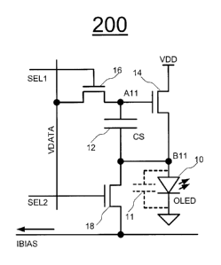
[0012] Figure 1 is a diagram showing a pixel circuit in accordance with an
embodiment
of the present invention;
[0013] Figure 2 is a timing diagram showing exemplary waveforms applied to the
pixel
circuit of Figure 1;
[0014] Figure 3 is a timing diagram showing further exemplary waveforms
applied to
the pixel circuit of Figure 1;
[0015] Figure 4 is a graph showing a current stability of the pixel circuit of
Figure 1;
[0016] Figure 5 is a diagram showing a pixel circuit which has p-type
transistors and
corresponds to the pixel circuit of Figure 1;
[0017] Figure 6 is a timing diagram showing exemplary waveforms applied to the
pixel
circuit of Figure 5;
[0018] Figure 7 is a timing diagram showing further exemplary waveforms
applied to
the pixel circuit of Figure 5;
[0019] Figure 8 is a diagram showing a pixel circuit in accordance with a
further
embodiment of the present invention;
[0020] Figure 9 is a timing diagram showing exemplary waveforms applied to the
pixel
circuit of Figure 8;
[0021] Figure 10 is a diagram showing a pixel circuit which has p-type
transistors and
corresponds to the pixel circuit of Figure 8;
[0022] Figure 11 is a timing diagram showing exemplary waveforms applied to
the
pixel circuit of Figure 10;
[0023] Figure 12 is a diagram showing a pixel circuit in accordance with an
embodiment of the present invention;
3
CA 02523841 2005-11-15
[0024] Figure 13 is a timing diagram showing exemplary waveforms applied to
the
display of Figure 12;
[0025] Figure 14 is a graph showing the settling time of a CBVP pixel circuit
for
different bias currents;
[0026] Figure 15 is a graph showing I-V characteristic of the CBVP pixel
circuit as well
as the total error induced in the pixel current;
[0027] Figure 16 is a diagram showing a pixel circuit which has p-type
transistors and
corresponds to the pixel circuit of Figure 12;
[0028] Figure 17 is a timing diagram showing exemplary waveforms applied to
the
display of Figure 16;
[0029] Figure 18 is a diagram showing a VBCP pixel circuit in accordance with
a
further embodiment of the present invention;
[0030] Figure 19 is a timing diagram showing exemplary waveforms applied to
the
pixel circuit of Figure 18;
[0031] Figure 20 is a diagram showing a VBCP pixel circuit which has p-type
transistors and corresponds to the pixel circuit of Figure 18;
[0032] Figure 21 is a timing diagram showing exemplary waveforms applied to
the
pixel circuit of Figure 20;
[0033] Figure 22 is a diagram showing a driving mechanism for a display array
having
CBVP pixel circuits; and
[0034] Figure 23 is a diagram showing a driving mechanism for a display array
having
VBCP pixel circuits.
DETAILED DESCRIPTION OF THE PREFERRED EMBODIMENTS OF THE
INVENTION
[0035] Embodiments of the present invention are described using a pixel having
an
organic light emitting diode (OLED) and a driving thin film transistor (TFT).
However,
4
CA 02523841 2005-11-15
the pixel may include any light emitting device other than OLED, and the pixel
may
include any driving transistor other than TFT. It is noted that in the
description, "pixel
circuit" and "pixel" may be used interchangeably.
[0036] A driving technique for pixels, including a current-biased voltage-
programmed
(CBVP) driving scheme, is now described in detail. The CBVP driving scheme
uses
voltage to provide for different gray scales (voltage programming), and uses a
bias to
accelerate the programming and compensate for the time dependent parameters of
a
pixel, such as a threshold voltage shift and OLED voltage shift.
[0037] Figure 1 illustrates a pixel circuit 200 in accordance with an
embodiment of the
present invention. The pixel circuit 200 employs the CBVP driving scheme as
described below. The pixel circuit 200 of Figure 1 includes an OLED 10, a
storage
capacitor 12, a driving transistor 14, and switch transistors 16 and 18. Each
transistor
has a gate terminal, a first terminal and a second terminal. In the
description, "first
terminal" ("second terminal") may be, but not limited to, a drain terminal or
a source
terminal (source terminal or drain terminal).
[0038] The transistors 14, 16 and 18 are n-type TFT transistors. The driving
technique
applied to the pixel circuit 200 is also applicable to a complementary pixel
circuit
having p-type transistors as shown in Figure 5.
[0039] The transistors 14, 16 and 18 may be fabricated using amorphous
silicon,
nano/micro crystalline silicon, poly silicon, organic semiconductors
technologies (e.g.
organic TFTs), NMOS technology, or CMOS technology (e.g. MOSFET). A plurality
of pixel circuits 200 may form an AMOLED display array.
[0040] Two select lines SEL1 and SEL2, a signal line VDATA, a bias line IBIAS,
a
voltage supply line VDD, and a common ground are provided to the pixel circuit
200.
In Figure 1, the common ground is for the OLED top electrode. The common
ground is
not a part of the pixel circuit, and is formed at the final stage when the
OLED 10 is
formed.
[0041] The first terminal of the driving transistor 14 is connected to the
voltage supply
line VDD. The second terminal of the driving transistor 14 is connected to the
anode
5
CA 02523841 2005-11-15
electrode of the OLED 10. The gate terminal of the driving transistor 14 is
connected
to the signal line VDATA through the switch transistor 16. The storage
capacitor 12 is
connected between the second and gate terminals of the driving transistor 14.
[0042] The gate terminal of the switch transistor 16 is connected to the first
select line
SEL1. The first terminal of the switch transistor 16 is connected to the
signal line
VDATA. The second terminal of the switch transistor 16 is connected to the
gate
terminal of the driving transistor 14.
[0043] The gate terminal of the switch transistor 18 is connected to the
second select
line SEL2. The first terminal of transistor 18 is connected to the anode
electrode of the
OLED 10 and the storage capacitor 12. The second terminal of the switch
transistor 18
is connected to the bias line IBIAS. The cathode electrode of the OLED 10 is
connected
to the common ground.
[0044] The transistors 14 and 16 and the storage capacitor 12 are connected to
node
All. The OLED 10, the storage capacitor 12 and the transistors 14 and 18 are
connected to B 11.
[0045] The operation of the pixel circuit 200 includes a programming phase
having a
plurality of programming cycles, and a driving phase having one driving cycle.
During
the programming phase, node B 11 is charged to negative of the threshold
voltage of the
driving transistor 14, and node A11 is charged to a programming voltage VP.
[0046] As a result, the gate-source voltage of the driving transistor 14 is:
VGS = VP - (-VT) = VP + VT (1)
where VGS represents the gate-source voltage of the driving transistor 14, and
VT
represents the threshold voltage of the driving transistor 14. This voltage
remains on
the capacitor 12 in the driving phase, resulting in the flow of the desired
current through
the OLED 10 in the driving phase.
[0047] The programming and driving phases of the pixel circuit 200 are
described in
detail. Figure 2 illustrates one exemplary operation process applied to the
pixel circuit
200 of Figure 1. In Figure 2, VnodeB represents the voltage of node B 11, and
VnodeA
6
CA 02523841 2005-11-15
represents the voltage of node Al l. As shown in Figure 2, the programming
phase has
two operation cycles X11, X12, and the driving phase has one operation cycle
X13.
[0048] The first operation cycle X11: Both select lines SEL1 and SEL2 are
high. A bias
current IB flows through the bias line IBIAS, and VDATA goes to a bias voltage
VB.
[0049] As a result, the voltage of node B11 is:
VnodeB = VB - [ILB - VT (2)
where VnodeB represents the voltage of node B 11, VT represents the threshold
voltage
of the driving transistor 14, and 0 represents the coefficient in current-
voltage (I-V)
characteristics of the TFT given by IDS =(3 (VGS - VT)2. IDS represents the
drain-source current of the driving transistor 14.
[0050] The second operation cycle X12: While SEL2 is low, and SEL1 is high,
VDATA goes to a programming voltage VP. Because the capacitance 11 of the OLED
is large, the voltage of node B 11 generated in the previous cycle stays
intact.
[0051 ] Therefore, the gate-source voltage of the driving transistor 14 can be
found as:
15 VGS=VP+4VB+VT (3)
AVB = f!_VB (4)
[0052] AVB is zero when VB is chosen properly based on (4). The gate-source
voltage
of the driving transistor 14, i.e., VP+VT, is stored in the storage capacitor
12.
[0053] The third operation cycle X13: IBIAS goes to low. SEL1 goes to zero.
The
20 voltage stored in the storage capacitor 12 is applied to the gate terminal
of the driving
transistor 14. The driving transistor 14 is on. The gate-source voltage of the
driving
transistor 14 develops over the voltage stored in the storage capacitor 12.
Thus, the
current through the OLED 10 becomes independent of the shifts of the threshold
voltage of the driving transistor 14 and OLED characteristics.
7
CA 02523841 2005-11-15
[0054] Figure 3 illustrates a further exemplary operation process applied to
the pixel
circuit 200 of Figure 1. In Figure 3, VnodeB represents the voltage of node B
11, and
VnodeA represents the voltage of node A11.
[0055] The programming phase has two operation cycles X21, X22, and the
driving
phase has one operation cycle X23. The first operation cycle X21 is same as
the first
operation cycle X11 of Figure 2. The third operation cycle X33 is same as the
third
operation cycle X 13 of Figure 2. In Figure 3, the select lines SEL1 and SEL2
have the
same timing. Thus, SEL1 and SEL2 may be connected to a common select line.
[0056] The second operating cycle X22: SELI and SEL2 are high. The switch
transistor 18 is on. The bias current IB flowing through IBIAS is zero.
[0057] The gate-source voltage of the driving transistor 14 can be VGS = VP +
VT as
described above. The gate-source voltage of the driving transistor 14, i.e.,
VP+VT, is
stored in the storage capacitor 12.
[0058] Figure 4 illustrates a simulation result for the pixel circuit 200 of
Figure 1 and
the waveforms of Figure 2. The result shows that the change in the OLED
current due
to a 2-volt VT-shift in the driving transistor (e.g. 14 of Figure 1) is almost
zero percent
for most of the programming voltage. Simulation parameters, such as threshold
voltage, show that the shift has a high percentage at low programming voltage.
[0059] Figure 5 illustrates a pixel circuit 202 having p-type transistors. The
pixel
circuit 202 corresponds to the pixel circuit 200 of Figure 1. The pixel
circuit 202
employs the CBVP driving scheme as shown in Figures 6-7. The pixel circuit 202
includes an OLED 20, a storage capacitor 22, a driving transistor 24, and
switch
transistors 26 and 28. The transistors 24, 26 and 28 are p-type transistors.
Each
transistor has a gate terminal, a first terminal and a second terminal.
[0060] The transistors 24, 26 and 28 may be fabricated using amorphous
silicon,
nano/micro crystalline silicon, poly silicon, organic semiconductors
technologies (e.g.
organic TFTs), PMOS technology, or CMOS technology (e.g. MOSFET). A plurality
of pixel circuits 202 may form an AMOLED display array.
8
CA 02523841 2005-11-15
[0061 ] Two select lines SEL1 and SEL2, a signal line VDATA, a bias line
IBIAS, a
voltage supply line VDD, and a common ground are provided to the pixel circuit
202.
[0062] The transistors 24 and 26 and the storage capacitor 22 are connected to
node
A12. The cathode electrode of the OLED 20, the storage capacitor 22 and the
transistors 24 and 28 are connected to B 12. Since the OLED cathode is
connected to the
other elements of the pixel circuit 202, this ensures integration with any
OLED
fabrication.
[0063] Figure 6 illustrates one exemplary operation process applied to the
pixel circuit
202 of Figure 5. Figure 6 corresponds to Figure 2. Figure 7 illustrates a
further
exemplary operation process applied to the pixel circuit 202 of Figure 5.
Figure 7
corresponds to Figure 3. The CBVP driving schemes of Figures 6-7 use IBIAS and
VDATA similar to those of Figures 2-3.
[0064] Figure 8 illustrates a pixel circuit 204 in accordance with an
embodiment of the
present invention. The pixel circuit 204 employs the CBVP driving scheme as
described below. The pixel circuit 204 of Figure 8 includes an OLED 30,
storage
capacitors 32 and 33, a driving transistor 34, and switch transistors 36, 38
and 40. Each
of the transistors 34, 35 and 36 includes a gate terminal, a first terminal
and a second
terminal. This pixel circuit 204 operates in the same way as that of the pixel
circuit 200.
[0065] The transistors 34, 36, 38 and 40 are n-type TFT transistors. The
driving
technique applied to the pixel circuit 204 is also applicable to a
complementary pixel
circuit having p-type transistors, as shown in Figure 10.
[0066] The transistors 34, 36, 38 and 40 may be fabricated using amorphous
silicon,
nano/micro crystalline silicon, poly silicon, organic semiconductors
technologies (e.g.
organic TFTs), NMOS technology, or CMOS technology (e.g. MOSFET). A plurality
of pixel circuits 204 may form an AMOLED display array.
[0067] A select line SEL, a signal line VDATA, a bias line IBIAS, a voltage
line VDD,
and a common ground are provided to the pixel circuit 204.
[0068] The first terminal of the driving transistor 34 is connected to the
cathode
electrode of the OLED 30. The second terminal of the driving transistor 34 is
connected
9
CA 02523841 2005-11-15
to the ground. The gate terminal of the driving transistor 34 is connected to
its first
terminal through the switch transistor 36. The storage capacitors 32 and 33
are in series
and connected between the gate of the driving transistor 34 and the ground.
[0069] The gate terminal of the switch transistor 36 is connected to the
select line SEL.
The first terminal of the switch transistor 36 is connected to the first
terminal of the
driving transistor 34. The second terminal of the switch transistor 36 is
connected to the
gate terminal of the driving transistor 34.
[0070] The gate terminal of the switch transistor 38 is connected to the
select line SEL.
The first terminal of the switch transistor 38 is connected to the signal line
VDATA.
The second terminal of the switch transistor 38 is connected to the connected
terminal
of the storage capacitors 32 and 33 (i.e. node C21).
[0071 ] The gate terminal of the switch transistor 40 is connected to the
select line SEL.
The first terminal of the switch transistor 40 is connected to the bias line
IBIAS. The
second terminal of the switch transistor 40 is connected to the cathode
terminal of the
OLED 30. The anode electrode of the OLED 30 is connected to the VDD.
[0072] The OLED 30, the transistors 34, 36 and 40 are connected at node A21.
The
storage capacitor 32 and the transistors 34 and 36 are connected at node B21.
[0073] The operation of the pixel circuit 204 includes a programming phase
having a
plurality of programming cycles, and a driving phase having one driving cycle.
During
the programming phase, the first storage capacitor 32 is charged to a
programming
voltage VP plus the threshold voltage of the driving transistor 34, and the
second
storage capacitor 33 is charged to zero
[0074] As a result, the gate-source voltage of the driving transistor 34 is:
VGS= VP+VT (5)
where VGS represents the gate-source voltage of the driving transistor 34, and
VT
represents the threshold voltage of the driving transistor 34.
[0075] The programming and driving phases of the pixel circuit 204 are
described in
detail. Figure 9 illustrates one exemplary operation process applied to the
pixel circuit
CA 02523841 2005-11-15
204 of Figure 8. As shown in Figure 9, the programming phase has two operation
cycles X31, X32, and the driving phase has one operation cycle X33.
[0076] The first operation cycle X3 1: The select line SEL is high. A bias
current IB
flows through the bias line IBIAS, and VDATA goes to a VB-VP where VP is and
programming voltage and VB is given by:
VB = IFLB (6)
[0077] As a result, the voltage stored in the first capacitor 32 is:
VCI = VP + VT (7)
where VCl represents the voltage stored in the first storage capacitor 32, VT
represents
the threshold voltage of the driving transistor 34, 0 represents the
coefficient in
current-voltage (I-V) characteristics of the TFT given by IDS =(3(VGS -VT)2.
IDS
represents the drain-source current of the driving transistor 34.
[0078] The second operation cycle: While SEL is high, VDATA is zero, and IBIAS
goes to zero. Because the capacitance 31 of the OLED 30 and the parasitic
capacitance
of the bias line IBIAS are large, the voltage of node B21 and the voltage of
node A21
generated in the previous cycle stay unchanged.
[0079] Therefore, the gate-source voltage of the driving transistor 34 can be
found as:
VGS=VP+VT (8)
where VGS represents the gate-source voltage of the driving transistor 34..
[0080] The gate-source voltage of the driving transistor 34 is stored in the
storage
capacitor 32.
[0081] The third operation cycle X33: IBIAS goes to zero. SEL goes to zero.
The
voltage of node C21 goes to zero. The voltage stored in the storage capacitor
32 is
applied to the gate terminal of the driving transistor 34. The gate-source
voltage of the
driving transistor 34 develops over the voltage stored in the storage
capacitor 32.
11
CA 02523841 2005-11-15
Considering that the current of driving transistor 34 is mainly defined by its
gate-source
voltage, the current through the OLED 30 becomes independent of the shifts of
the
threshold voltage of the driving transistor 34 and OLED characteristics.
[0082] Figure 10 illustrates a pixel circuit 206 having p-type transistors.
The pixel
circuit 206 corresponds to the pixel circuit 204 of Figure 8. The pixel
circuit 206
employs the CBVP driving scheme as shown in Figure 11. The pixel circuit 206
of
Figure 10 includes an OLED 50, a storage capacitors 52 and 53, a driving
transistor 54,
and switch transistors 56, 58 and 60. The transistors 54, 56, 58 and 60 are p-
type
transistors. Each transistor has a gate terminal, a first terminal and a
second terminal.
[0083] The transistors 54, 56, 58 and 60 may be fabricated using amorphous
silicon,
nano/micro crystalline silicon, poly silicon, organic semiconductors
technologies (e.g.
organic TFTs), PMOS technology, or CMOS technology (e.g. MOSFET). A plurality
of pixel circuits 206 may form an AMOLED display array.
[0084] Two select lines SEL1 and SEL2, a signal line VDATA, a bias line IBIAS,
a
voltage supply line VDD, and a common ground are provided to the pixel circuit
206.
The common ground may be same as that of Figure 1.
[0085] The anode electrode of the OLED 50, the transistors 54, 56 and 60 are
connected
at node A22. The storage capacitor 52 and the transistors 54 and 56 are
connected at
node B22. The switch transistor 58, and the storage capacitors 52 and 53 are
connected
at node C22.
[0086] Figure 11 illustrates one exemplary operation process applied to the
pixel circuit
206 of Figure 10. Figure 11 corresponds to Figure 9. As shown in Figure 11,
the CBVP
driving scheme of Figure 11 uses IBIAS and VDATA similar to those of Figure 9.
[0087] Figure 12 illustrates a display 208 in accordance with an embodiment of
the
present invention. The display 208 employs the CBVP driving scheme as
described
below. In Figure 12, elements associated with two rows and one column are
shown as
example. The display 208 may include more than two rows and more than one
column.
[0088] The display 208 includes an OLED 70, storage capacitors 72 and 73,
transistors
76, 78, 80, 82 and 84. The transistor 76 is a driving transistor. The
transistors 78, 80
12
CA 02523841 2005-11-15
and 84 are switch transistors. Each of the transistors 76, 78, 80, 82 and 84
includes a
gate terminal, a first terminal and a second terminal.
[0089] The transistors 76, 78, 80, 82 and 84 are n-type TFT transistors. The
driving
technique applied to the pixel circuit 208 is also applicable to a
complementary pixel
circuit having p-type transistors, as shown in Figure 16.
[0090] The transistors 76, 78, 80, 82 and 84 maybe fabricated using amorphous
silicon,
nano/micro crystalline silicon, poly silicon, organic semiconductors
technologies (e.g.
organic TFTs), NMOS technology, or CMOS technology (e.g. MOSFET). The display
208 may form an AMOLED display array. The combination of the CBVP driving
scheme and the display 208 provides a large-area, high-resolution AMOLED
display.
[0091] The transistors 76 and 80 and the storage capacitor 72 are connected at
node
A3 1. The transistors 82 and 84 and the storage capacitors 72 and 74 are
connected at
B31.
[0092] Figure 13 illustrates one exemplary operation process applied to the
display 208
of Figure 12. In Figure 13, "Programming cycle [n]" represents a programming
cycle
for the row [n] of the display 208.
[0093] The programming time is shared between two consecutive rows (n and
n+l).
During the programming cycle of the nth row, SEL[n] is high, and a bias
current IB is
flowing through the transistors 78 and 80. The voltage at node A31 is self-
adjusted to
(IB/(3)1/2+VT, while the voltage at node B31 is zero, where VT represents the
threshold
voltage of the driving transistor 76, and 0 represents the coefficient in
current-voltage
(I-V) characteristics of the TFT given by IDS =[3 (VGS - VT)2, and IDS
represents the
drain-source current of the driving transistor 76.
[0094] During the programming cycle of the (n+l)th row, VDATA changes to VP-
VB.
As a result, the voltage at node A31 changes to VP+VT if VB =(IB/(3)1/2. Since
a
constant current is adopted for all the pixels, the IBIAS line consistently
has the
appropriate voltage so that there is no necessity to pre-charge the line,
resulting in
shorter programming time and lower power consumption. More importantly, the
voltage of node B31 changes from VP-VB to zero at the beginning of the
programming
13
CA 02523841 2005-11-15
cycle of the nth row. Therefore, the voltage at node A31 changes to
(IB/0)1/2+VT, and
it is already adjusted to its final value, leading to a fast settling time.
[0095] The settling time of the CBVP pixel circuit is depicted in Figure 14
for different
bias currents. A small current can be used as IB here, resulting in lower
power
consumption.
[0096] Figure 15 illustrates I-V characteristic of the CBVP pixel circuit as
well as the
total error induced in the pixel current due to a 2-V shift in the threshold
voltage of a
driving transistor (e.g. 76 of Figure 12). The result indicates the total
error of less than
2% in the pixel current. It is noted that IB=4.5 A.
[0097] Figure 16 illustrates a display 210 having p-type transistors. The
display 210
corresponds to the display 208 of Figure 12. The display 210 employs the CBVP
driving scheme as shown in Figure 17. In Figure 12, elements associated with
two rows
and one column are shown as example. The display 210 may include more than two
rows and more than one column.
[0098] The display 210 includes an OLED 90, a storage capacitors 92 and 94,
and
transistors 96, 98, 100, 102 and 104. The transistor 96 is a driving
transistor. The
transistors 100 and 104 are switch transistors. The transistors 24, 26 and 28
are p-type
transistors. Each transistor has a gate terminal, a first terminal and a
second terminal.
[0099] The transistors 96, 98, 100, 102 and 104 may be fabricated using
amorphous
silicon, nano/micro crystalline silicon, poly silicon, organic semiconductors
technologies (e.g. organic TFTs), PMOS technology, or CMOS technology (e.g.
MOSFET). The display 210 may form an AMOLED display array.
[00100] In Figure 16, the driving transistor 96 is connected between the anode
electrode of the OLED 90 and a voltage supply line VDD.
[00101] Figure 17 illustrates one exemplary operation process applied to the
display 210 of Figure 16. Figure 17 corresponds to Figure 13. The CBVP driving
scheme of Figure 17 uses IBIAS and VDATA similar to those of Figure 13.
14
CA 02523841 2005-11-15
[00102] According to the CBVP driving scheme, the overdrive voltage provided
to the driving transistor is generated so as to be independent from its
threshold voltage
and the OLED voltage.
[00103] The shift(s) of the characteristic(s) of a pixel element(s) (e.g. the
threshold voltage shift of a driving transistor and the degradation of a light
emitting
device under prolonged display operation) is compensated for by voltage stored
in a
storage capacitor and applying it to the gate of the driving transistor. Thus,
the pixel
circuit can provide a stable current though the light emitting device without
any effect
of the shifts, which improves the display operating lifetime. Moreover,
because of the
circuit simplicity, it ensures higher product yield, lower fabrication cost
and higher
resolution than conventional pixel circuits.
[00104] Since the settling time of the pixel circuits described above is much
smaller than conventional pixel circuits, it is suitable for large-area
display such as high
definition TV, but it also does not preclude smaller display areas either.
[00105] It is noted that a driver for driving a display array having a CBVP
pixel
circuit (e.g. 200, 202 or 204) converts the pixel luminance data into voltage.
[00106] A driving technique for pixels, including voltage-biased
current-programmed (VBCP) driving scheme is now described in detail. In the
VBCP
driving scheme, a pixel current is scaled down without resizing mirror
transistors. The
VBCP driving scheme uses current to provide for different gray scales (current
programming), and uses a bias to accelerate the programming and compensate for
a
time dependent parameter of a pixel, such as a threshold voltage shift. One of
the
terminals of a driving transistor is connected to a virtual ground VGND. By
changing
the voltage of the virtual ground, the pixel current is changed. A bias
current IB is
added to a programming current IP at a driver side, and then the bias current
is removed
from the programming current inside the pixel circuit by changing the voltage
of the
virtual ground.
[00107] Figure 18 illustrates a pixel circuit 212 in accordance with a further
embodiment of the present invention. The pixel circuit 212 employs the VBCP
driving
scheme as described below. The pixel circuit 212 of Figure 18 includes an OLED
I 10,
CA 02523841 2005-11-15
a storage capacitor 111, a switch network 112, and mirror transistors 114 and
116. The
mirror transistors 114 and 116 form a current mirror. The transistor 114 is a
programming transistor. The transistor 116 is a driving transistor. The switch
network
112 includes switch transistors 118 and 120. Each of the transistors 114, 116,
118 and
120 has a gate terminal, a first terminal and a second terminal.
[00108] The transistors 114, 116, 118 and 120 are n-type TFT transistors. The
driving technique applied to the pixel circuit 212 is also applicable to a
complementary
pixel circuit having p-type transistors as shown in Figure 20.
[00109] The transistors 114, 116, 118 and 120 may be fabricated using
amorphous silicon, nano/micro crystalline silicon, poly silicon, organic
semiconductors
technologies (e.g. organic TFTs), NMOS technology, or CMOS technology (e.g.
MOSFET). A plurality of pixel circuits 212 may form an AMOLED display array.
[00110] A select line SEL, a signal line IDATA, a virtual grand line VGND, a
voltage supply line VDD, and a common ground are provided to the pixel circuit
150.
[00111] The first terminal of the transistor 116 is connected to the cathode
electrode of the OLED 110. The second terminal of the transistor 116 is
connected to
the VGND. The gate terminal of the transistor 114, the gate terminal of the
transistor
116, and the storage capacitor 111 are connected to a connection node A4 1.
[00112] The gate tenninals of the switch transistors 118 and 120 are connected
to
the SEL. The first terminal of the switch transistor 120 is connected to the
IDATA. The
switch transistors 118 and 120 are connected to the first terminal of the
transistor 114.
The switch transistor 118 is connected to node A41.
[00113] Figure 19 illustrates an exemplary operation for the pixel circuit 212
of
Figure 18. Referring to Figures 18 and 19, current scaling technique applied
to the pixel
circuit 212 is described in detail. The operation of the pixel circuit 212 has
a
programming cycle X41, and a driving cycle X42.
[00114] The programming cycle X41: SEL is high. Thus, the switch transistors
118 and 120 are on. The VGND goes to a bias voltage VB. A current (IB+IP) is
provided through the IDATA, where IP represents a programming current, and IB
16
CA 02523841 2005-11-15
represents a bias current. A current equal to (IB+IP) passes through the
switch
transistors 118 and 120.
[00115] The gate-source voltage of the driving transistor 116 is self-adjusted
to:
VGS = /iP + IB + VT (9)
where VT represents the threshold voltage of the driving transistor 116, and
(3
represents the coefficient in current-voltage (I-V) characteristics of the TFT
given by
IDS =(3(VGS -VT)2. IDS represents the drain-source current of the driving
transistor
116.
[00116] The voltage stored in the storage capacitor 111 is:
VCS = I+IB_VB+VT ~(10)
where VCS represents the voltage stored in the storage capacitor I 11.
[00117] Since one terminal of the driving transistor 116 is connected to the
VGND, the current flowing through the OLED I 10 during the programming time
is:
Ipixel =IP+IB+/3=(VB)2 -2~fi =VB (IP+IB) (11)
where Ipixel represents the pixel current flowing through the OLED 110.
[00118] If IB >> IP, the pixel current Ipixel can be written as:
Ipixel =IP+(IB+,l3=(VB)2 -2J6 - VB IB) (12)
[00119] VB is chosen properly as follows:
VB = r (13)
[00120] The pixel current Ipixel becomes equal to the programming current IP.
Therefore, it avoids unwanted emission during the programming cycle.
17
CA 02523841 2005-11-15
[00121] Since resizing is not required, a better matching between two mirror
transistors in the current-mirror pixel circuit can be achieved.
[00122] Figure 20 illustrates a pixel circuit 214 having p-type transistors.
The
pixel circuit 214 corresponds to the pixel circuit 212 of Figure 18. The pixel
circuit 214
employs the VBCP driving scheme as shown Figure 21. The pixel circuit 214
includes
an OLED 130, a storage capacitor 131, a switch network 132, and mirror
transistors 134
and 136. The mirror transistors 134 and 136 form a current mirror. The
transistor 134
is a programming transistor. The transistor 136 is a driving transistor. The
switch
network 132 includes switch transistors 138 and 140. The transistors 134, 136,
138 and
140 are p-type TFT transistors. Each of the transistors 134, 136, 138 and 140
has a gate
terminal, a first terminal and a second terminal.
[00123] The transistors 134, 136, 138 and 140 maybe fabricated using
amorphous silicon, nano/micro crystalline silicon, poly silicon, organic
semiconductors
technologies (e.g. organic TFTs), PMOS technology, or CMOS technology (e.g.
MOSFET). A plurality of pixel circuits 214 may form an AMOLED display array.
[00124] A select line SEL, a signal line IDATA, a virtual grand line VGND, and
a voltage supply line VSS are provided to the pixel circuit 214.
[00125] The transistor 136 is connected between the VGND and the cathode
electrode of the OLED 130. The gate terminal of the transistor 134, the gate
terminal
of the transistor 136, the storage capacitor 131 and the switch network 132
are
connected at node A42.
[00126] Figure 21 illustrates an exemplary operation for the pixel circuit 214
of
Figure 20. Figure 21 corresponds to Figure 19. The VBCP driving scheme of
Figure
21 uses IDATA and VGND similar to those of Figure 19.
[00127] The VBCP technique applied to the pixel circuit 212 and 214 is
applicable to current programmed pixel circuits other than current mirror type
pixel
circuit.
18
CA 02523841 2005-11-15
[00128] For example, the VBCP technique is suitable for the use in AMOLED
displays. The VBCP technique enhances the settling time of the current-
programmed
pixel circuits display, e.g. AMOLED displays.
[00129] It is noted that a driver for driving a display array having a VBCP
pixel
circuit (e.g. 212, 214) converts the pixel luminance data into current.
[00130] Figure 22 illustrates a driving mechanism for a display array 150
having
a plurality of CBVP pixel circuits 151 (CBVP1-1, CBVP1-2, CBVP2-1, CBVP2-2).
The CBVP pixel circuit 151 is a pixel circuit to which the CBVP driving scheme
is
applicable. For example, the CBVP pixel circuit 151 may be the pixel circuit
shown in
Figure 1, 5, 8, 10, 12 or 16. In Figure 22, four CBVP pixel circuits 151 are
shown as
example. The display array 150 may have more than four or less than four CBVP
pixel
circuits 151.
[00131] The display array 150 is an AMOLED display where a plurality of the
CBVP pixel circuits 151 are arranged in rows and columns. VDATAI (or VDATA 2)
and IBIAS 1(or IBIAS2) are shared between the common column pixels while SEL1
(or
SEL2) is shared between common row pixels in the array structure.
[00132] The SEL1 and SEL2 are driven through an address driver 152. The
VDATAI and VDATA2 are driven through a source driver 154. The IBIASI and
IBIAS2 are also driven through the source driver 154. A controller and
scheduler 156
is provided for controlling and scheduling programming, calibration and other
operations for operating the display array, which includes the control and
schedule for
the CBVP driving scheme as described above.
[00133] Figure 23 illustrates a driving mechanism for a display array 160
having
a plurality of VBCP pixel circuits. In Figure 23, the pixel circuit 212 of
Figure 18 is
shown as an example of the VBCP pixel circuit. However, the display array 160
may
include any other pixel circuits to which the VBCP driving scheme described is
applicable.
[00134] SEL1 and SEL2 of Figure 23 correspond to SEL of Figure 18. VGNDI
and VGAND2 of Figure 23 correspond to VDATA of Figure 18. IDATA1 and IDATA
19
CA 02523841 2006-03-10
2 of Figure 23 correspond to IDATA of Figure 18. In Figure 23, four VBCP pixel
circuits are shown as example. The display array 160 may have more than four
or less
than four VBCP pixel circuits.
[00135] The display array 160 is an AMOLED display where a plurality of the
VBCP pixel circuits are arranged in rows and columns. IDATAI (or IDATA2) is
shared between the common column pixels while SELl (or SEL2) and VGND1 (or
VGND2) are shared between common row pixels in the array structure.
[00136] The SELl, SEL2, VGND1 and VGND2 are driven through an address
driver 162. The IDATAI and IDATA are driven through a source driver 164. A
controller and scheduler 166 is provided for controlling and scheduling
programming,
calibration and other operations for operating the display array, which
includes the
control and schedule for the VBCP driving scheme as described above.
[00137] The present invention has been described with regard to one or more
embodiments. However, it will be apparent to persons skilled in the art that a
number
of variations and modifications can be made without departing from the scope
of the
invention as defmed in the claims.