Note: Descriptions are shown in the official language in which they were submitted.
CA 02527911 2009-11-30
27844-65
- 1 -
"Superconducting quantum antenna"
The present invention relates to an active highly
sensitive antenna for electromagnetic waves, that includes
at least one superconducting quantum interference filter
or at least one low temperature transistor.
Prior art:
The mode of operation of conventional electric
receiving antennas is based essentially on the fact
that an incident electromagnetic wave induces a voltage
drop across the antenna that constitutes the input
signal for the receiving electronics. However, the
induced voltage drop is generally so small that it must
initially be amplified with the aid of resonance
effects. In this case, either the conventional antenna
is itself designed in such a way that a geometrical
resonance occurs at the receiving frequency, or the
antenna is provided with an electric balancing network
such that the antenna and balancing network form a
resonant circuit.
Owing to the resonance amplification required for
achieving an adequate sensitivity, the frequency
bandwidth within which reception is possible is
severely restricted with conventional antennas. The
bandwidth is typically smaller than 20% of the
resonance frequency. A larger bandwidth can be achieved
with the aid of so-called "frequency independent"
logarithmic spiral antennas. However, even here the
extent of the antenna must be in the region of the
wavelength of the electromagnetic wave to be received,
and the sensitivity of such antennas is mostly low.
It is true in principle that magnetic loop antennas can
be designed with broader bands than electric antennas,
but they cannot be used at relatively high frequencies
because of the occurrence of inductive effects and
because of the skin effect. Moreover, during
CA 02527911 2009-11-30
27844-65
2 -
conventional operation the impedance of magnetic loop
antennas can be adapted to the impedance of
conventional electronic circuits only with difficulty,
and the efficiency of the antennas is thereby sharply
decreased.
A further problem occurs with conventional antenna
systems when electromagnetic waves of very low signal
strength are to be received. The input sensitivity of
conventional antenna systems is limited in principle by
the noise of the preamplifier following the antenna.
The input signal coming from the antenna must be above
the noise threshold of the preamplifier so that it can
be usefully amplified. In order to receive very small
signals, it is therefore necessary with conventional
receiving systems that the antenna extracts a
sufficient amount of energy from the electromagnetic
field. In the case of very small signal strengths, this
can be achieved conventionally only by using very large
antennas, parabolic mirrors or arrays of antennas, for
example. In any case, the spatial extent of the antenna
increases sharply here. A typical application in which
small signal strengths are present, is the reception of
satellite signals, for example. Here, the extent of the
antenna is typically in the region of one meter.
Because of their large dimensions, antenna arrays are
not suitable, or suitable only in a severely restricted
way, for mobile use, in particular, for example in
vehicles, ships or aircraft.
Since conventional antenna systems must extract energy
from the electromagnetic field in order to process the
information contained in the field, the range of
transmission antennas :is additionally limited in
principle by the number of the receivers for a given
transmitter power.
CA 02527911 2009-11-30
27844-65
- 3 -
Some embodiments of the present invention may address the
problem of overcoming the limitations of conventional receiving antennas with
regard to their sensitivity and their dimensions.
According to one broad aspect, the present invention provides an
antenna for radio-frequency electromagnetic waves, comprising: normally
conductive and/or superconducting electrical circuitry with one or more active
components, the active components comprising at least one transistor, which is
suitable for use at low temperatures; a primary antenna structure; means for
supplying the circuitry with electrical power; means for supplying the
circuitry with
a control current and/or a control voltage; means for emitting an
electromagnetic
wave from the circuitry; an active cooler which can extract heat from at least
a part
of the circuitry during operation; and a vacuum vessel which contains at least
a
part of the circuitry and at least a part of the primary antenna structure and
by
means of which this part can be thermally isolated from the surrounding area,
wherein the vacuum vessel contains a cooling finger of the active cooler,
wherein
the cooling finger is thermally coupled to at least one normally conductive
and/or
superconducting waveguide termination of the primary antenna structure,
wherein
the active components are thermally coupled to the cooling finger, wherein the
active components are electromagnetically coupled to the waveguide
termination,
wherein the vacuum vessel has a window through which electromagnetic waves
can pass and is geometrically designed such that an electromagnetic wave can
be
fed into the waveguide termination, and wherein the active cooler is designed
to
cool at least a part of the circuitry below a low temperature of 150 Kelvin.
Some of the potential advantages that may be provided by some
embodiments of the invention reside in the fact that owing to its functional
principle when using a superconducting quantum interference filter, in
CA 02527911 2009-11-30
27844-65
- 3a -
particular, the antenna extracts no energy, or only a
very small amount thereof, from the electromagnetic
field and thereby renders possible the reception of
very small signals in conjunction with a very small
dimension of the antenna itself. In order to achieve
the sensitivity of a parabolic antenna of approximately
60 cm diameter, an inventive antenna of approximately
1 cm x 1 cm is typically sufficient. In addition, the
antenna can be designed such that its bandwidth is
bounded only by the cutoff frequency of the
superconducting quantum interference filter used. This
cutoff frequency is typically in the range of 20 GHz to
100 GHz, and so appropriate bandwidths can be achieved.
A superconducting quantum interference filter has the
following basic features:
closed superconducting cells which form a current loop
and in each case include a plurality of, preferably two
Josephson junctions,
at least three of these cells are connected in a
superconducting or non-superconducting fashion,
the junctions of the at least three cells can be
energized in such a way that a time-variant voltage
drops in each case across at least two junctions of a
cell, the time average of which voltage does not
vanish,
CA 02527911 2009-11-30
27844-65
4 -
closed superconducting cells that form a current loop
and in each case include a plurality, preferably two
Josephson junctions,
at least three of these cells are connected in a
superconducting or non-superconducting fashion,
the junctions of the at least three cells can be
energized in such a way that a time-variant voltage
drops in each case across at least two junctions of a
cell, the time average of which voltage does not
vanish,
the at least three cells are configured differently
geometrically in such a way that the magnetic fluxes
enclosed by the cells in the case of an existing
magnetic field differ from one another in such a way
that the frequency spectrum of the voltage response
function has no significant (Do-periodic component with
reference to the magnetic flux, or in that if a
discrete frequency spectrum exists, the contribution of
the (Do-periodic component of the discrete frequency
spectrum is not dominant compared to the non-periodic
components of the discrete frequency spectrum.
Specific reference is made here to the corresponding
German laid-open patent application and to the US
patent. A description is given herein not only of the
described basic form of a superconducting quantum
interference filter, also denoted below as a SQIF, but
also to a multiplicity of developments corresponding to
the following statements A.1) to A12).
CA 02527911 2005-12-01
-
when the magnetic fluxes enclosed by the cells are not
in a rational ratio to one another. In addition, the
differences in area between the individual cells are
preferably relatively large. In particular, in this
5 case cells connected in a superconducting fashion are
superimposed in such a way that the voltage response
function no longer has a period.
Consequently, different cells are connected to one
another specifically, and this is something the person
skilled in the art would always want to avoid with
conventional SQUID arrangements. This is expressed, for
example, in the publication by HANSEN, BINSLEV J.,
LINDELOF P.E.: Static and dynamic interactions between
Josephson junctions. In: Reviews of Modern Physics,
Vol. 56, No. 3, July 1984, p. 431 to 459. On page 434,
left-hand column, last paragraph and subsequently in
the right-hand column, this publication favors a system
with identical cells and identical junctions and, by
contrast, classifies asymmetries as counterproductive
for the functioning of the SQUID described in this
regard.
Superconducting quantum interference filters exhibit
the physical effect of multiple macroscopic quantum
interference in such a way that the ambiguity of the
calibration curves of conventional SQUID magnetometers
and SQUID gradiometers is removed.
In a superconducting quantum interference filter, the
quantum mechanical wave functions which describe the
state of the superconducting solid interfere in such a
way that a unique macroscopic calibration curve (V(B;Io))
is produced. In the ideal case, the calibration curve
(V(B;Io)) of the superconducting quantum interference
filter has no periodicity with the period (Do and is a
function, rising monotonically in a specific measuring
CA 02527911 2005-12-01
6 -
range, of the absolute value of the external magnetic
field B at the location of the SQIF.
The uniqueness of the calibration curve, and the high
sensitivity of superconducting quantum interference
filters permit the direct measurement of time-variant
electromagnetic fields in a continuous frequency range
whose lower bound is at vext 0 and whose upper bound
is currently at several hundred GHz to THz, depending
on the type of Josephson junctions or weak links used.
This entire frequency range is accessible with the aid
of a single, appropriately designed superconducting
quantum interference filter. In the detection of
electromagnetic waves, the superconducting quantum
interference filter operates simultaneously as a
receiving antenna, filter and powerful amplifier. The
inherent noise of suitably designed quantum
interference filters can in this case be smaller by
several orders of magnitude than the inherent noise of
conventional SQUID magnetometers. A further advantage
by comparison with conventional antennas and filters
resides in this case in that, inter alia, depending on
the measuring principle the frequency range is not a
function of the spatial extent of the superconducting
quantum interference filter. The spatial extent can
influence only the sensitivity.
The production of superconducting quantum interference
filters can be performed using known, cost-effective
technical methods such as are applied, for example, in
modern production of conventional SQUIDs. Since the
spatial extent of superconducting quantum interference
filters need not differ substantially from the spatial
extent of conventional SQUID systems, the
cryotechnologies developed for conventional SQUID
systems can be taken over directly. There is no need
for specific developments in the field of
cryotechnology.
CA 02527911 2005-12-01
7 -
A2) In a system made from the cells described above,
it is preferable to provide at least for one cell,
favorably for the largest part of the cells, exactly
two junctions per cell which are connected in a
superconducting fashion and connected electrically in
parallel. The effects just described can be achieved
comparatively simply and effectively by exactly two
junctions.
A3) However, the desired effects can also be achieved
in a favorable way when more than two junctions are
provided in a cell which are connected in a
superconducting fashion and connected electrically in
parallel, specifically in the form of a series circuit
of junctions which is connected in parallel to an
individual junction, or in the form of two parallel-
connected series circuits of junctions.
A4) However, the effects according to the invention
can also be achieved by structures of at least one cell
of a network, in the case of which, in addition to a
basic form of at least two junctions across which a
time-variant voltage whose time average does not vanish
drops, in particular in addition to a basic form of two
junctions connected electrically in parallel, a further
junction or a plurality of further junctions are
provided, which contacts are not directly energized and
therefore there is no voltage drop on average across
these junctions. In this case, the connections of all
the junction in the individual cells continue to be
superconducting. Such embodiments can be advantageous,
since the screening currents induced in the individual
cells by a magnetic field can be reduced by additional
junctions. The influence of self-inductances and mutual
inductances can thereby be reduced.
A5) In a particularly preferred embodiment, a
plurality of cells form a network or a network section,
in which all junctions are connected electrically in
CA 02527911 2005-12-01
8 -
parallel such that the junctions can be energized in
the same direction. In particular, particularly high
sensitivities for the measurement of a magnetic field
can be achieved by means of such an arrangement when,
in this connection, the cells are interconnected in a
superconducting fashion.
A6) A plurality of cells or network sections can,
however, also be advantageously connected electrically
in series such that the junctions in the network can in
turn be energized in the same direction. The magnitude
of the measurement signal can be increased by this
measure, since the voltages at the junctions add
together in the series circuit.
A7) A particularly high sensitivity can also be
achieved by the parallel connection of series
arrangements of a plurality of cells or network
sections. In this embodiment, the network sections or
cells are preferably connected in a superconducting
fashion, in particular by means of superconducting
twisted-pair cables. The resolution capacity of
superconducting quantum interference filters can in
this case reach down to the range of aT (10-18 tesla)
and below. The calibration curve also remains unique
for such measuring ranges, thus rendering possible
absolute quantitative measurements of extremely small
fields.
A8) The network can be used in a voltage-driven or
current-driven fashion.
A9) In order to achieve Josephson effects which are as
ideal as possible, it is proposed, furthermore, that
the junctions are designed as point junctions.
A10) In order to increase the sensitivity of a SQIF,
it is further possible for the geometry of the cell
arrangement to be designed so as to reduce magnetic
CA 02527911 2005-12-01
9 -
crosstalk from one cell to an adjacent cell on the
basis of the magnetic self-field produced by a current
flowing in the cells.
All) In a further preferred refinement, the cells of
the network and/or network sections are spatially
aligned, in particular in two-dimensional or three-
dimensional space. This measure renders it possible to
determine individual magnetic field components in
addition to the absolute value of the magnetic field.
The direction of the magnetic field can therefore be
measured in the case of a three-dimensional arrangement
in space.
A12) It is further preferred if the current driving
the junctions is fed in, and/or led off again through
ohmic resistors which are designed, in particular, as
busbar resistors. The point is that measurements have
shown that the performance of the SQIF can be
substantially improved by feeding the driving current
through ohmic resistors.
For further refinements of the SQIFs, reference is made
to figures 9a to 20 and their associated parts of the
description in conjunction with the description of the
figures relating to figures 1 to 8.
If the superconducting quantum interference filter is
produced using high-temperature superconduction
technology, there is no problem in using miniature
coolers for permanent and reliable provision of the
operating temperature. These miniature coolers
typically have dimensions in the region of 10 cm and
require powers of less than 20 W, and so it is possible
to implement compact antenna systems that also permit
the mobile use of the antenna in the most varied
applications.
The antenna uses the physical phenomenon of multiple
CA 02527911 2005-12-01
- 10 -
macroscopic quantum interference to enhance
sensitivity. This phenomenon occurs in superconducting
circuits that have a special geometry. In the case of
the superconducting quantum interference filter, it is
used to implement a high power, low noise broadband
amplifier. In the simplest case, this amplifier is
inductively coupled to a primary, passive antenna
structure. Upon incidence of an electromagnetic wave,
an antenna current flows in this primary antenna
structure. This antenna current generates a magnetic
field that permeates the superconducting quantum
interference filter. If the superconducting quantum
interference filter is suitably supplied with electric
current and operated at a suitable operating point, a
voltage that depends on the strength of the magnetic
field and thus on the strength of the antenna current
then drops across the superconducting quantum
interference filter. Since the excitation of the
superconducting quantum interference filter is caused
by the quantum mechanical constraint of the so-called
flux quantization, during this process no amount of
energy, or only a very small one, is transferred from
the primary antenna structure to the superconducting
quantum interference filter. The power that is required
in order to generate the voltage drop across the
superconducting quantum interference filter is drawn
from the current source that supplies the
superconducting quantum interference filter with
operating current. By contrast with conventional
antennas, there is no need for energy to be drawn from
the antenna, and thus from the incident wave, in order
to excite the superconducting quantum interference
filter. The reactive currents alone are sufficient for
an excitation. The primary antenna is not subjected to
loading during the transmission of the information
contained in the electromagnetic wave to the
superconducting quantum interference filter. Since no
energy flows from the primary antenna to the
superconducting quantum interference filter, there is
CA 02527911 2005-12-01
- 11 -
no need for impedance matching. This renders it
possible to implement extremely broadband receiving
antennas of very high sensitivity when use is made of
appropriate primary antenna structures.
The primary antenna structure can be composed in this
case of superconducting conductor pieces or of normally
conducting conductor pieces. A combination of the two
is also possible. Superconducting conductor pieces have
the advantage that a very high antenna current flows,
but in the case of resonance the resonance is very
narrowband as a rule. A lesser antenna current
typically flows in normally conducting conductor
pieces, but the resonances are more broadband.
Consequently, a respectively optimum primary antenna
structure can be designed depending on the application
and required sensitivity.
In order to achieve a high sensitivity of the antenna,
the primary antenna structure must be coupled with
sufficient strength to the superconducting quantum
interference filter. In the simplest case, this can be
achieved for a single-ply layer structure by virtue of
the fact that the part of the primary antenna that is
to be coupled into the superconducting quantum
interference filter is guided as tightly as possible
past the loops of the superconducting quantum
interference filter and has as small a conductor cross
section as possible. The magnetic field generated by
the antenna current then has a maximum value at the
location of the loops. Generally speaking, the coupling
is always particularly advantageous whenever the
current density distribution of the primary antenna
currents is very great or maximum at the location of as
many loops of the superconducting quantum interference
filter as possible, or in their vicinity. A decoupling
structure is provided in order to derive the voltage
oscillation (output signal of the antenna) dropping
across the superconducting quantum interference filter
CA 02527911 2005-12-01
- 12 -
in the presence of a time-variant antenna current, and
to pass it on to a consumer (receiver). This decoupling
structure is used to convert the voltage oscillation
into an electromagnetic wave that is passed on to the
consumer with the aid of a suitable waveguide such that
parasitic losses can be kept as small as possible.
Because of their intrinsic robustness and fault
tolerance, superconducting quantum interference filters
are particularly well suited as secondary antenna
structures or integrated preamplifiers. They offer a
range of substantial advantages by comparison with
conventional superconducting magnetic field voltage
transformers. In particular, superconducting quantum
interference filters have a unique characteristic by
contrast with conventional SQUIDs or SQUID arrays.
Whereas in the case of SQUIDs or SQUID arrays it is
necessary because of the periodicity of the
characteristic to take particular precautions to shield
parasitic magnetic fields, this is not necessary in
principle with superconducting quantum interference
filters. Again, the transfer factor between magnetic
field and dropping voltage can basically be adapted in
any required way to the amplifier task to be solved.
Because of the robustness of superconducting quantum
interference filters, the magnetic field coupled into
the superconducting quantum interference filter by the
primary antenna structures need not fulfill any
condition of homogeneity. The superconducting quantum
interference filter can even be excited by strongly
inhomogeneous magnetic fields without power loss. In
addition, because of their high intrinsic tolerance to
parameter imperfections superconducting quantum
interference filters are much easier to produce than
are SQUID arrays, for example. The intrinsic fault
tolerance also has the consequence that the most varied
superconducting materials can be used.
A first important aspect of the invention relates to an
CA 02527911 2005-12-01
- 13 -
antenna for electromagnetic waves composed of at least
one superconducting quantum interference filter,
primary antenna structures made from normally
conducting and/or superconducting materials in which an
antenna current is induced upon incidence of an
electromagnetic wave, of means for generating an
adjustable magnetic field for controlling the
superconducting quantum interference filter, of means
for supplying the superconducting quantum interference
filter with an operating current and of means that are
designed to be able to derive as electromagnetic wave a
voltage oscillation dropping across the superconducting
quantum interference filter, wherein the primary
antenna structure is electrically connected to the
superconducting quantum interference filter and/or is
magnetically coupled thereto, and the superconducting
quantum interference filter is supplied with an
operating current in such a way and the magnetic field
for controlling the superconducting quantum
interference filter can be adjusted in such a way that
the antenna current flowing in the antenna structure
upon incidence of electromagnetic waves excites the
superconducting quantum interference filter such that
an electric voltage dependent on the antenna current
drops across the superconducting quantum interference
filter.
An advantageous refinement of the invention provides
that the antenna includes additional means for driving
a suitable operating point on the characteristic of the
superconducting quantum interference filter (for
example energizable control lines, magnetic field
coils). This renders it possible to operate the
superconducting quantum interference filter in a region
of the characteristic in which the latter amplifies a
signal optimally. In addition, it is possible to drive
a region of high linearity of the characteristic in
order to minimize undesired intermodulation products.
The frequency of the voltage dropping across the
CA 02527911 2005-12-01
- 14 -
superconducting quantum interference filter is
identical to the frequency of the antenna current at
such an operating point.
It is advantageous for receiving electromagnetic waves
of high frequency when the output of the
superconducting quantum interference filter is
connected to the conventional electronics of the
antenna system as directly as possible, that is to say
with the smallest possible lead length. This can be
achieved with the aid of low temperature transistors
such as, for example, HEMT or MOSFET. These can be
operated in the cold part of the antenna system, that
is to say where the low temperature required for
operating the superconducting quantum interference
filter prevails. Such a circuit must be thermally
insulated at least partially, for example by being
arranged at least partially in a vacuum chamber so that
it can be brought to the suitable operating temperature
by active or passive cooling elements. Suitable in
particular as cooling elements are both liquid gases
such as, for example, liquid nitrogen or liquid helium,
and active coolers such as, for example, Sterling,
Joule-Thomson, or pulse tube coolers. These cooling
elements can be designed with the aid of methods known
from the prior art such that they can extract a
sufficient quantity of heat from the thermally
insulated part of the circuit and/or parts of the
primary antenna structure during operation.
The nature of the thermally insulated part of the
primary antenna structure at at least one location is
such that it is transparent to an electromagnetic wave
of the desired frequency. Depending on the frequency
range in which the antenna is intended to operate, this
so-called window can consist of various materials such
as, for example, Teflon, silica glass, aluminum oxide,
ceramic etc.
CA 02527911 2005-12-01
- 15 -
The appropriate electric supply and control lines are
provided for operating the superconducting quantum
interference filter and the low temperature transistor.
These lines should preferably be routed in the region
of the thermally insulated part of the circuit in such
a way that the heat input from these lines is not too
large.
In addition, means are provided for leading off the
electromagnetic wave from the circuit. Typically, this
is done for high frequencies initially with the aid of
microstriplines and then with coaxial cables or other
suitable waveguides. However, it is also possible when
passing the wave through the thermal insulation to make
use of contact-free transitions, for example capacitive
couplers.
Superconducting high frequency lines are preferably
provided for functionally connecting up primary antenna
structure, superconducting quantum interference filter
and low temperature transistor, since they are not, or
only minimally, affected by losses. However, it can
also be advantageous, for example for reasons of cost,
to use normally conducting lines or hollow conductors,
since these are easier to produce. Since these lines
are located at least partially in the region of the
thermally insulated part of the circuit and thus are at
a very low temperature, even in the case of normally
conducting lines there is a substantial advantage over
conventional circuits with regard to dissipative
losses.
Embodiments in which the lines are normally conducting
and superconducting can also be advantageous. If
superconducting strip lines are provided with an
additional normally conducting coating, the lines can
be dimensioned such that the current flows off via the
normally conducting part in the case of overloading or
of a short circuit, and the superconductor thereby
CA 02527911 2005-12-01
- 16 -
suffers no damage.
Since antenna systems typically must have a very high
level of dynamics, it can be advantageous, moreover, if
superconducting quantum interference filters and low
temperature transistors can be operated independently
of one another in different branches of the circuit.
Given the presence of large input signals for which the
superconducting quantum interference filter would go
into saturation, the branch thereof can be shut down
and only the transistor branch can be operated. Given
the presence of very small input signals, by contrast,
use is made of the branch of the circuit that includes
the superconducting quantum interference filter.
Thus, it is also possible to conceive an antenna system
that uses only the advantages of a low temperature
transistor, and therefore comprises no superconducting
quantum interference filter.
Again, when it is constructed from normally conducting
or from normally conducting and superconducting high
frequency conductors and includes a branch composed of
low temperature transistors without superconducting
quantum interference filters, the antenna system can
already be operated at temperatures that are higher
than the transition temperature of the superconductors
used. This has the advantage that less cooling power is
required for relatively large input signals, and yet a
higher sensitivity is achieved by comparison with
transistors operated at normal temperature.
Consequently, the sensitivity of the antenna system can
be adjusted variably by the temperature by means of a
variably adjustable extraction of heat, as is possible
without any problem with active coolers, for example.
Since a substantial part of the dissipative losses are
caused by power losses in the case of conventional
circuits, it is additionally advantageous likewise to
CA 02527911 2005-12-01
- 17 -
cool at least the high frequency lines that from the
primary antenna structure to the respectively first
active component, that is to say superconducting
quantum interference filter or low temperature
transistor.
A very effective form of thermal insulation is, for
example, accommodating the circuit or parts of the
circuit in an evacuatable chamber. Such chambers can be
designed such that they maintain the vacuum and thus
the thermal insulation over a number of years.
Particularly when active coolers are used, a cooling
finger can be mounted in a vacuum chamber cost
effectively and in a space saving fashion.
The thermal insulation of the circuit or parts of the
circuit is advantageously itself already designed as
part of the primary antenna structure. This can be
performed, for example, by using dielectric material
(for example Teflon foam) for the thermal insulation
and fashioning the latter geometrically such that the
incident electromagnetic wave can be focused onto the
superconducting quantum interference filter or another
coupling structure. Again, the thermal insulation can
be performed by means of a metallic vacuum chamber. The
metallic vacuum chamber itself can then, in turn, be
designed as part of the primary antenna structure. For
example, the metallic vacuum chamber can be designed as
a waveguide or waveguide termination supplied from a
primary aperture. Again, the vacuum chamber can
advantageously be provided with high frequency windows
that act as primary aperture antennas.
In a preferred embodiment, the entire dissipative
losses and thus the inherent noise of the system can be
minimized by thermal insulation and cooling of the
entire circuit composed of superconducting quantum
interference filter, low temperature transistor and
primary antenna structure. This produces an apparatus
CA 02527911 2005-12-01
- 18 -
with maximum performance.
In a particularly advantageous embodiment, especially
for the GHz frequency range, the decoupling part of the
primary antenna structure is designed as a hollow
conductor termination into which an elongated antenna
element, for example an antenna pin projects. With the
aid of this antenna pin electrically insulated from the
hollow conductor, the electromagnetic wave is decoupled
directly with low loss, particularly when the hollow
conductor termination is at a low temperature, or is
transported to the input of an active component with
the aid of a suitable line. By connecting a plurality
of active components in series, it is already possible
to achieve in the cold part of the circuit an
amplification of the antenna signal that is of very low
noise. The thermal insulation of the circuit and of the
hollow conductor termination is advantageously
performed by means of an evacuatable chamber.
In a development of the embodiment described in the
last paragraph, the hollow conductor termination is
provided with two, in particular pin-shaped, antenna
elements that are fitted offset from one another. This
has the advantage that two independent polarizations
can be decoupled from the hollow conductor separately
from one another. The separate coupling to in each case
one active component permits the separate processing of
the two polarizations.
For applications in which the overall space of the
antenna system is to be as small as possible, it is
advantageous to use arrays of aperture or slot antennas
as primary antenna structure, particularly in the range
of GHz frequencies.
Because of the high sensitivity of superconducting
quantum interference filters, the size of the overall
aperture is generally given in the case of antenna
CA 02527911 2005-12-01
- 19 -
arrays only by the desired directional characteristic
of the antenna system. The physical aperture can
therefore be composed both of one-dimensional, two-
dimensional and of three-dimensional arrays of primary
antennas. The assembly of the output signals of the
individual antennas of the antenna array can be
performed by means of a structure of hollow conductors
or microstriplines. Particularly powerful antenna
systems also result when the primary antenna structure
is composed of superconductors, particularly when the
output signals of the individual antennas of the array
are assembled with the aid of superconducting high
frequency lines. If use is made in such arrays of
additional active components such as, for example,
phase shifters to control the directional
characteristic, a further advantage arises since these
components also produce very much less noise at low
temperatures, and operate more efficiently.
The directional characteristic of the antenna system
can also be modeled very effectively with the aid of
primary antenna structures that are designed as arrays
of patch antennas. In particular, a separation of
polarization can already be performed on the plane of
the individual antennas given appropriate design of the
individual antennas of the antenna array.
The use of electromagnetic lenses as primary antenna
structure is advantageous when signals of different
polarization or signals with temporally variant
polarization are to be received simultaneously by the
antenna system. Since electromagnetic lenses retain the
polarization of the incident wave, tracking on the
plane of the primary antenna structure is eliminated in
the event of temporal changes in the polarization of
the incident wave.
For applications in which very large instantaneous
bandwidths are required, it is advantageous to use horn
CA 02527911 2005-12-01
- 20 -
antennas as primary antenna structure. By means of
appropriately dimensioned hollow conductor structures,
the output signal of the horn antennas can be coupled
very efficiently to a superconducting quantum
interference filter.
Very large instantaneous bandwidths can also be
achieved by using parabolic antennas. Given the same
effective aperture, a quantum antenna thus designed is
more powerful by a multiple than a conventional
parabolic antenna of the same size, particularly in the
GHz frequency range. In addition, a very high
directional effect of the antenna system can be
achieved with the aid of arrays of parabolic antennas.
In a further advantageous refinement of the invention,
the electrodes of the superconducting quantum
interference filter themselves are designed as the
primary antenna structures. This refinement has the
advantage that the magnetic field of the antenna
current flowing in these structures is coupled directly
into the loops of the superconducting quantum
interference filter. The extent of the antenna can
thereby be further reduced.
Since the superconducting quantum interference filter
can have different impedances depending on the type of
Josephson junctions used, it is advantageous,
furthermore, to equip the antenna circuit with an
impedance transformer which transforms the impedance of
the superconducting quantum interference filter to the
impedance of a waveguide that leads off the signal.
It is known that the Josephson junctions that the
superconducting quantum interference filter includes
are nonlinear oscillators in which a high frequency
oscillating current flows. It is likewise known that
such Josephson oscillators can also be synchronized
(lock) onto the frequency of an externally irradiated
CA 02527911 2005-12-01
- 21 -
wave. Because of the Josephson relation, the DC voltage
dropping across the junctions is then rigorously
proportional to the frequency of the irradiated wave.
If the information to be received in the incident wave
is coded via the frequency (frequency modulation), the
time characteristic of the DC voltage dropping across
the junctions and thus of the DC voltage dropping
across the superconducting quantum interference filter
then corresponds to the information content of the
incident wave. Because of the uniqueness of the
characteristic of the superconducting quantum
interference filter, the frequency of the Josephson
oscillation in the superconducting quantum interference
filter can be adjusted very exactly by appropriate
selection of the operating current supplying the
superconducting quantum interference filter, and of a
magnetic control field. On the one hand, it is thereby
ensured that the superconducting quantum interference
filter locks onto the carrier frequency of the incident
wave, while on the other hand this frequency can be
changed very easily.
In all cases where the carrier frequency oscillates
quickly by comparison with the modulation frequency,
the received signal is automatically demodulated in
this operating mode of the antenna, and can be
processed further directly. The embodiment specified in
claim 5 is therefore suitable in particular for the
frequency range between 1 GHz and 100 GHz and is very
advantageous because the conventionally required
downmixing of the signal with the aid of local
oscillators is eliminated.
Moreover, because of the simpler method of production,
it is advantageous when the primary antenna structure
and the superconducting quantum interference filter are
located on a common carrier (chip). This permits the
fabrication of integrated antenna chips with the aid of
known methods of thin film technology.
CA 02527911 2005-12-01
- 22 -
In specific wavelength regions and given the use of
materials that do not permit multilayer technology, it
can, however, also be advantageous to apply the two
functional elements of the antenna to different
carriers. These carriers can then be coupled with the
aid of electric wires. This arrangement is also
advantageous when the primary antenna structure is to
be aligned spatially in a fashion other than the
superconducting quantum interference filter because of
the overall space, because of the reduction of external
interference or because of other reasons. A further
advantage consists in that different materials can be
used for the different carriers.
When the antenna must have a very high sensitivity and
no multilayer technology is available, it is also
possible to achieve efficient coupling between primary
antenna structure and superconducting quantum
interference filter by virtue of the fact that the
carriers of the two functional elements are fitted
directly one above another and, for example, bonded to
one another.
Superconducting electronic components require very low
operating temperatures. The outlay required for
producing and maintaining these temperatures rises very
sharply the lower the operating temperature of the
superconductors used. In principle, all known
superconductors from which it is possible to produce
Josephson junctions can be used for the antennas.
However, it is advantageous to use materials in the
case of which the operating temperature is as high as
possible. These known materials are so-called high
temperature superconductors whose operating
temperatures reach over approximately -200 C and that
can be cooled cost effectively with the aid of liquid
nitrogen. The known simplest and most cost effective
method of producing Josephson junctions from such
CA 02527911 2005-12-01
- 23 -
materials is the method of grain boundary junctions.
Although these junctions have very inhomogeneous
parameters and are therefore otherwise very little
suited to quantum electronic circuits, because of the
design-induced very high fault tolerance of
superconducting quantum interference filters they can,
however, be used without any problem in the case of the
antenna.
Moreover, it is advantageous when the primary antenna
structures also consist of high temperature
superconductors. Since a super conductor has the
property that electric fields vanish completely in its
interior, higher antenna currents flow as a rule in
such structures than in normally conducting structures.
This increases the sensitivity of the antenna.
If the antenna consists of superconductors or of
superconductors and normal conductors, it can also be
operated actively, that is to say with the aid of a
cooler, without the use of liquid coolants. Whereas
liquid coolants must be replaced regularly and the
operating times are thereby very restricted, coolers
can make the required operating temperatures available
permanently and reliably. Because of the use of
superconducting quantum interference filters that have
a very high level of dynamics, the electromagnetic
interference caused by the coolers does not lead to a
loss in performance of the antenna. Given the use of
high temperature superconductors, the typical powers
that are required to operate a cooler are very low and
are in the range of 20 W - 40 W. Such powers can also
be made available in mobile use, mostly without any
problems.
During operation of the antenna in a cooler, it is
favorable when the antenna is located on a chip that is
fitted directly on the cooling finger of the cooler.
The required cooling power is substantially reduced
CA 02527911 2005-12-01
- 24 -
thereby, and it is possible to use very small coolers.
The required cooling power is further reduced when the
output signal of the antenna is led off the antenna
chip with the aid of a waveguide that conducts heat
poorly.
Moreover, it is advantageous when the waveguide is used
simultaneously for supplying the antenna with electric
energy. This saves additional cables that would
increase the thermal loading and thus the required
cooling power.
Particularly in the case of receive frequencies in the
GHz range, it is advantageous for the primary antenna
structure to be of resonant design. This is done in the
simplest way by using antenna rods or arrays whose
length is in the region of half the wavelength of the
incident wave. In this case, large reactive currents
flow in the antenna structures, something which sharply
increases the sensitivity of the antenna. It is also
possible in this case to use patch or patch-like
antennas whose dimensions are in the region of half the
wavelength of the incident wave.
Since no impedance matching of the primary antenna
structure is required, it is also possible to use
magnetic loop antennas as primary antenna structures.
Since the superconducting quantum interference filter
is extremely low in noise, such loop antennas can also
be used up to very high frequencies. The advantage of
loop antennas resides here in that their dimensions can
be very much smaller than the wavelength of the
incident wave. Since it is only the antenna currents
that are important, both open and closed loop antennas
can be used.
Because of the very high sensitivity of superconducting
quantum interference filters, it is also possible to
use individual or arrays of electrically small
CA 02527911 2005-12-01
- 25 -
antennas. The dimensions of such primary antennas are
certainly smaller than the wavelength of the incident
wave, but even without a matching network the antenna
currents induced in them generally suffice to excite
the superconducting quantum interference filter
sufficiently.
For specific applications, in particular in the case of
very high frequencies, it can also be advantageous to
use a dielectric layer as primary antenna structure.
Instances of resonance likewise occur in such layers,
and surface currents flow that can be coupled into the
superconducting quantum interference filter.
Combinations of dielectric layers with conducting
structures are also possible.
The primary antenna structure can also be composed of a
resonant cavity inside which the superconducting
quantum interference filter is fitted at a suitable
location on maximum magnetic field strength. Specific
modes can then be selected depending on the position of
the superconducting quantum interference filter inside
the cavity. This can be advantageous, in particular,
for polarization separation and for further enhancement
of the sensitivity.
If frequency filter elements are additionally fitted in
the primary antenna structure or between primary
antenna structure and superconducting quantum
interference filter, appropriate frequency bands can
then be selected in a targeted fashion. It is thereby
possible to implement a multiband antenna. This can be
of great advantage whenever very large differences
prevail in the signal strengths of the incident waves
simultaneously in different frequency bands.
Excessively strong signals in specific bands that would
mask the weak signals to be received can thereby be
eliminated.
CA 02527911 2005-12-01
- 26 -
The performance of the antenna can be enhanced by
installing additional active and/or passive electronic
components. This is the case, in particular, when the
transfer of the output signal of the antenna to the
conventional receiving electronics is to be performed
directly at the output of the superconducting quantum
interference filter in order to avoid parasitic losses.
Propagation time losses can be minimized thereby, in
particular in the case of very high frequencies. Since
the antenna itself takes up only very little overall
space, the additional electronic components can be
accommodated in the cold part of the circuit. Given
appropriate selection of the components, there is thus
a substantial reduction in the thermal noise, and the
sensitivity of the overall system of antenna and
receiver rises.
The sensitivity can also be increased by the use of two
or more inventive antennas in an antenna array. Such
antenna arrays can be cooled jointly by a cooler, or
each antenna has its own cooler. Antenna arrays have
the advantage that the sensitivity of the overall
system rises sharply with the number of antennas used
(supergain). In addition, strongly pronounced
directional characteristics can, moreover, be produced
by an appropriate arrangement of the individual
antennas in the array (superdirectivity).
If inventive antennas are arranged in an antenna array,
and the output signals of the individual antennas are
superposed in a phase-sensitive fashion with the aid of
suitable means such as, for example, electronically
controllable phase shifters or delay lines, to form an
aggregate signal, this has the advantage, furthermore,
that the spatial position of the transmitter of the
received electromagnetic wave can be determined very
exactly. If the location of the transmitter is known,
this method can be used, on the other hand, to
discriminate between different transmitters. Since
CA 02527911 2005-12-01
- 27 -
inventive antennas draw no energy, or only a very
slight amount, from the electromagnetic field, the
determination of the position of inventive antennas is,
by contrast, exceptionally difficult.
A particularly cost effective and efficacious
production method for the antenna can be used whenever
the circuit is designed using the known microstripline
technology. In this technology, electrode and counter-
electrode of the circuit are not both fitted on the
surface of a carrier (chip), but the carrier is
provided with a base plate that forms the counter-
electrode. It is then only the conductor tracks of the
electrode that are situated on the surface of the
carrier. This method permits a very high integration
density on the carrier and minimizes the losses because
the electric fields are substantially concentrated in
the substrate of the carrier. If the antenna chip is
operated on the cooling finger of an active cooler, it
is also possible for this cooling finger itself to be
used as base plate (counter-electrode).
Particularly at frequencies of less than 1 GHz, it is
advantageous to equip the superconducting quantum
interference filter with a feedback loop. In this case,
the output signal of the superconducting quantum
interference filter is fed back to the superconducting
quantum interference filter either positively - to
increase the sensitivity - or negatively - to stabilize
the operating point. In the case of negative feedback,
the circuit can be operated in this case such that the
operating point on the characteristic of the
superconducting quantum interference filter remains
constant. In this case, the feedback current or the
feedback voltage includes the information of the
incident wave.
Because of the reciprocity of reception and
transmission of electromagnetic waves, the antenna can
CA 02527911 2005-12-01
- 28 -
also be designed in such a way that it emits an
electromagnetic wave. If the impedance of the
superconducting quantum interference filter is tuned to
the radiation impedance of the primary antenna field,
the superconducting quantum interference filter then
impresses on the primary antenna array a voltage
oscillation fed into it. The primary antenna array then
emits an electromagnetic wave. It is true that the
emitted power is low in general because of the
functional principle of the antenna, but this
embodiment can be advantageous when, in addition to
reception, the aim is to fulfill still further tasks,
for example the synchronization of antennas operating
spatially separately from one another.
The following citations may be specified in relation to
the prior art:
J.D. Kraus, Antennas, 2nd Edition, McGraw-Hill, 1988.
S. Ramo, J.R. Whinnery, T. VanDuzer, Fields and waves
in communication electronics, 3rd edition, John Wiley,
1994.
A. Barone and G. Paterno, Physics and Applications of
the Josephson Effect, John Wiley, 1982.
J. Hinken, Superconducting Electronics, Springer, 1988.
K.K. Likharev, Dynamics of Josephson junctions and
circuits, Gordon and Breach, 1991.
R.D. Parmentier and N.F. Pedersen, Nonlinear
superconducting devices and High-Tc materials, World
Scientific, 1995.
J.C. Gallop et al., SQUIDS, the Josephson Effect and
superconducting electronics, Hilger, 1991.
H. Weinstock (editor), SQUID Sensors: Fundamentals,
Fabrication and Applications, Kluwer Academic Publishers,
1996.
J. Oppenlander, Ch. Hau2ler and N. Schopohl, Phys. Rev.
B63, 024511 (2001).
Ch. Haul3ler, J. Oppenlander and N. Schopohl, J. Appl.
Phys. 89, 1875 (2001).
J. Oppenlander, T. Trauble, Ch. Haul3ler and N. Schopohl,
CA 02527911 2005-12-01
- 29 -
IEEE Trans. Appl. Supercond. 11, 1271 (2001).
J. Oppenlander, Ch. Hauf3ler, T. Trauble and N. Schopohl,
Physica C 368, 119 (2002).
V. Schultze, R. Ijsselsteijn, H.-G. Meyer,
J. Oppenlander, Ch. HauBler and N. Schopohl, IEEE
Trans. Appl. Supercond. 13, (to appear June 2003).
Drawings:
A plurality of exemplary embodiments are illustrated in
the drawings and explained in more detail with a
specification of further advantages and details.
In the drawings:
figure 1 shows the typical magnetic field voltage
characteristic of a superconducting quantum
interference filter, and the definition of a suitable
operating point,
figure 2a shows a typical circuit design of an
inventive antenna with superconducting quantum
interference filter and coupled primary antenna
structure,
figure 2b shows an inventive antenna in the case of
which the electrodes of the superconducting quantum
interference filter are themselves designed as primary
antenna structures,
figure 2c shows an antenna circuit in the case of which
the output signal of the antenna is decoupled via a
coplanar impedance transformer,
figure 2d shows an antenna with grain boundary
Josephson junctions, designed using high temperature
superconducter technology,
figure 3 shows the diagrammatic illustration of the
operation of an inventive antenna in an active cooling
system,
figure 4a shows a primary antenna array with
geometrical resonance,
figure 4b shows an inventive antenna in the case of
which the primary antenna structure is designed as
resonant cavity,
CA 02527911 2005-12-01
- 30 -
figure 4c shows an antenna circuit designed using
microstrip technology,
figure 5 shows the highly diagrammatic illustration of
an antenna structure for electromagnetic waves of high
frequency,
figure 6 shows a diagrammatic illustration of an
antenna structure having a vacuum chamber,
figure 7a shows an embodiment comparable to figure 5
but having an array of aperture antennas,
figure 7b shows an embodiment in an illustration
corresponding to figure 7a an antenna having a
parabolic mirror,
figure 8 shows an embodiment of an antenna having an
array of patch antennas, in a diagrammatic illustration,
figures 9a and b show a multicell SQIF of parallel-
connected Josephson junctions, in a spatial
arrangement,
figure 10 shows the circuit diagram of an equivalent
superconducting circuit of a quantum interference
filter with N = 10 junctions,
figures 10a to f show circuit diagrams of further
superconducting circuits,
figure 11 shows a voltage response function for a SQIF
with N = 30 junctions,
figures 12a and b show periodic voltage response
functions for conventional SQUIDs,
figure 12c shows the voltage response function of a
superconducting quantum interference filter,
figure 12d shows the voltage response function of a
SQUID and a SQIF,
figure 13 shows a symbolically illustrated spatial
arrangement of a superconducting quantum interference
filter with an indication of the vector basis of the
three-dimensional space,
figure 14 shows a diagrammatically illustrated, flat
superconducting quantum interference filter with a
magnetic field compensation device,
CA 02527911 2005-12-01
- 31 -
figure 15 shows a superconducting quantum interference
filter with a parallel-connected control line, in a
diagrammatic view,
figure 16 shows a diagrammatically illustrated
networking of SQIF sections,
figures 17a to c show diagrammatically illustrated,
flat, superconducting quantum interference filters with
a geometrical arrangement for minimizing the influence
of self-fields,
figure 18a shows a network made from cells connected in
series,
figure 18b shows a voltage response function
corresponding to a network in accordance with
figure 18a, in the case of a series circuit for N = 100
cells,
figure 18c shows a current-voltage characteristic of a
network in accordance with figure 18a, when it is
operated as a current amplifier with the aid of a
compensation circuit,
figure 19a shows, in the top picture, the typical
voltage response function of a conventional SQUID with
the associated frequency spectrum in the bottom
picture,
figure 19b shows, in the top picture, a typical voltage
response function of a network made from identical
cells, and the associated frequency spectrum in the
bottom picture,
figure 19c shows, in the top picture, the voltage
response function of a superconducting quantum
interference filter without periodicity, and the
associated spectrum in the bottom picture,
figure 19d shows, in the top picture, a voltage
response function and, in the bottom picture, the
associated spectrum of a quantum interference filter
which has a technically conditioned, comparatively
large periodicity, and
figure 20 shows a diagrammatically illustrated, flat
superconducting quantum interference filter with a
superconducting pick-up loop which amplifies the
CA 02527911 2005-12-01
- 32 -
primary magnetic field at the location of the filter.
Description of the exemplary embodiments:
A typical characteristic of a superconducting quantum
interference filter (SQIF) is illustrated in figure 1.
If the SQIF is supplied with an electric current of
suitable strength, a voltage dependent on the magnetic
field that permeates the SQIF drops across the SQIF. By
contrast with the known, conventional SQUIDs, the
characteristic is not periodic, but has an unambiguous
minimum in the vanishing magnetic field B=O. Since the
characteristic is not sinusoidal, as with the
conventional SQUIDs or SQUID arrays, the linearity of
its edge 1 or 1* is very high. By setting a suitable
operating point 2, something which can be performed,
for example, by applying a constant magnetic field
(control field), the SQIF can be operated with high
linearity as an amplifier or as a current-to-voltage
converter.
A typical antenna circuit having the features of
claim 1 is illustrated in figure 2a. The SQIF 3 is
coupled inductively to a primary antenna 4. Upon
incidence of an electromagnetic wave, an antenna
current flows through the primary antenna 4. Since the
antenna is guided spatially in a specific region
tightly along the SQIF, this antenna current generates
a magnetic field at the location of the SQIF loops. If
the SQIF is operated at a suitable operating point 2, a
voltage whose direction depends on the direction of the
antenna current drops across the SQIF. In this way, the
SQIF generates a voltage oscillation that corresponds
to the oscillation of the antenna current. By suitable
selection of the number of the SQIF loops 3, it is
possible in principle to adjust the range of the
voltage dropping across the SQIF as desired, and thus
to select any desired dynamic range of the current-to-
voltage converter. The magnetic field required for
CA 02527911 2005-12-01
- 33 -
controlling the SQIF can result from a field coil or
from a control line 5 loaded with a suitable current.
This line can also be used to stabilize the operating
point or to feed back into the SQIF the voltage signal
generated by the SQIF, for example, with the aid of an
electric resistor. The electrodes 3a and 3b are fitted
on the SQIF so that the voltage oscillation dropping
across the SQIF can be passed on to a receiver. These
electrodes are connected to a waveguide suitable for
the respective frequency range and which passes on the
output signal of the SQIF to the receiver in a fashion
as free from loss as possible.
In the simplest case, the SQIF is operated without
controlling the operating point at the minimum of the
characteristic. The voltage signal generated by the
SQIF then has double the frequency of the oscillation
of the antenna current. It is possible, in particular,
in this operating mode of the antenna to receive binary
phase-coded signals very easily and reliably.
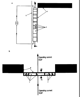
A parallel SQIF is designed in figure 2b in such a way
that the electrodes of the SQIF themselves constitute
the primary antenna structure. Upon incidence of an
electromagnetic wave of appropriate polarization, an
antenna current is induced in the electrode 6. This
antenna current couples a magnetic field directly into
the loops 7 of the SQIF. The output signal on the SQIF
is led off with the aid of the electrodes 7a and 7b.
The electrodes 6 can also be designed in this case as a
closed loop (an embodiment not illustrated). In an
embodiment that is likewise not illustrated, the
electrodes of the individual SQIF loops or of groups of
loops are constructed as respective individual antenna
rods or antenna structures. This embodiment has the
advantage that the individual antenna structures can be
of different design, and thus permit the bandwidth of
the antenna to be adjusted.
CA 02527911 2005-12-01
- 34 -
figure 2c illustrates an antenna circuit in the case of
which the output signal of the SQIF 8 is decoupled via
a coplanar stripline 9. Located at the end of the
coplanar stripline 9 is a coplanar impedance
transformer structure 10 that transforms the impedance
of the SQIF to the impedance of the directed waveguide
11. Losses owing to impedance matching of the SQIF and
waveguide or consumer (receiver circuit) can thereby be
avoided.
The primary antenna structure is composed in figure 2c
of antenna rods 12 at whose end a spiral winding 13 is
fitted. The spiral windings 13 are fitted directly
above the loops of the SQIF 14, something which is
possible, for example, without any problem in
multilayer thin film technology. The magnetic field
generated by the antenna currents is coupled very
effectively into the SQIF in such arrangements.
Illustrated in figure 2d is an antenna circuit in the
case of which the SQIF and primary antenna structure
have been produced from high temperature
superconductors (here YBCO) . The Josephson junctions
are grain boundary junctions here. These grain boundary
junctions arise when a conductor track 15 crosses the
grain boundary 16. Because of the simple design of the
junctions, the scatters of the junction parameters are
very high. By contrast with conventional quantum
electronic circuits, this does not, however, influence
the performance of the SQIF. The line 17 is part of the
primary antenna structure and coupled to the SQIF
inductively.
figure 3 shows an exemplary embodiment in which an
antenna chip is operated in a small cooler. The antenna
circuit 18 is located on chip. The chip itself is
thermally coupled to the cooling finger 19 of the small
cooler 20. The antenna chip and small cooler are
located in a vacuum flask 21 for the purpose of thermal
CA 02527911 2005-12-01
- 35 -
insulation. The vacuum flask 21 has a window 22
transparent to electromagnetic waves. The output signal
of the antenna is led off from the antenna chip via a
vacuum-tight waveguide 23 that is a poor conductor of
heat. Because of the large dynamic range of SQIFs, it
is possible to use coolers of the most varied design.
In an embodiment that is not illustrated, the cooling
finger on which the antenna chip is located is itself
designed as primary antenna structure. Since the
carrier (substrate) couples the cooling finger
magnetically and electrically to the SQIF in any case,
this embodiment has the advantage that it is not
mandatory for a primary antenna structure to be located
on the chip.
In figure 4a, the primary antenna array 24 is composed
of line pieces 25 whose length has been selected as
half the wavelength of the electromagnetic wave to be
received. This embodiment has the advantage that in the
case of resonance high reactive currents flow in the
antenna structure and thereby excite the SQIF 26
optimally. By appropriate design of the antenna array
with antenna pieces of easily distinguishable length or
easily distinguishable spacing from one another, it is
possible to model a frequency band within which the
antenna is particularly sensitive.
figure 4b illustrates an embodiment in the case of
which the SQIF 27 is located in a resonant cavity 28
(waveguide open at one end). In addition to the
enhancement of the sensitivity, this has the advantage
that specific electromagnetic modes, for example for
the purpose of polarization separation, can be selected
using the position of the SQIF relative to the cavity.
In an embodiment that is not illustrated, several or
many antennas are arranged in antenna arrays. This has
the advantage that the sensitivity grows with the
CA 02527911 2005-12-01
- 36 -
number of the antennas, supergain effects can be used,
and a specific directional characteristic can be
modeled.
In an embodiment that is likewise not illustrated, the
elements of such an antenna array are operated in a
phase-controlled fashion (phased array antenna). For
this purpose, suitable phase shifters are used to
superpose the output signals of the various antennas
having different phase angles. This has the advantage
that it is thereby possible to select the spatial
position of the transmitter of the received
electromagnetic wave. In particular, when the spacings
between the antennas in the antenna array are selected
incommensurably, it is possible to use a phase-
sensitive superposition of the output signals of the
various antennas of the antenna array to determine the
spatial position of the transmitter of the
electromagnetic wave. Because of the functional
principle based on a quantum mechanical effect, the
very high linearity of the active antenna and the low
operating temperature, the phase noise of antennas
according to the invention is very low. In addition to
the very high sensitive by comparison with conventional
antennas, this low phase noise is a further great
advantage of antennas according to the invention.
figure 4c illustrates an exemplary embodiment of the
antenna in microstripline technology. The SQIF 29 and
the primary antenna structure 30 are located on the top
side of a substrate 31. The electrically conducting
base plate 32 forms the counter-electrode. The voltage
dropping across the SQIF 29 on excitation is capped
between the electrode 33 and the base plate 32. The
electrode 34 serves the purpose of supplying power to
the SQIF and/or of connection to the base plate. In the
case of substrates that permit this, it is also
possible to make use for this purpose of plated-through
holes (vias) to the base plate. When use is made of
CA 02527911 2005-12-01
- 37 -
multi-layer technologies, the base plate (counter-
electrode) can also be formed by conducting layer
structures on the surface of the substrate.
If the active antenna or the antenna chip is operated
in an active cooling system, the cooling finger itself,
on which the active antenna is fitted, can also be used
as counter-electrode (base plate) . Since the cooling
finger typically consists of metals that conduct heat
very well, and therefore generally of materials that
are also very good electric conductors, such a design
has great advantages in terms of production
engineering.
Figure 5 illustrates an exemplary embodiment for
electromagnetic waves of high frequency. The primary
antenna structure is composed of a horn antenna 60 and
a hollow conductor termination 55 with antenna pin 54.
The antenna pin 54 decouples the incident wave from the
hollow conductor termination. The antenna pin 54 is
connected directly to the input of a superconducting
quantum interference filter 51. A further amplification
of the signal is achieved by a low temperature
transistor 52 that is connected as amplifier. The
superconducting quantum interference filter 51 and the
transistor 52 are interconnected via a microstripline
53a. The amplified signal is fed into a waveguide 56
via a further microstripline 53b. The hollow conductor
terminal 55 and the circuit composed of antenna pin,
superconducting quantum interference filter and low
temperature transistor are located inside a thermal
insulation 57 that has a high frequency window 59. The
waveguide 56 leaves the thermal insulation 57 via a
feed through 56a. The control and supply lines 61 of
the circuit are guided through the feed through 61a.
The circuit 51, 52, 53a, 53b is coupled via the hollow
conductor termination 55 and a thermal conductor 58 to
a cold reservoir (not illustrated) (passive cooling,
for example by means of liquid gas), or to an active
CA 02527911 2005-12-01
- 38 -
cooler (active cooling, for example Sterling or pulse
tube cooler).
The antenna pin 54 and the microstriplines 53 can be of
normally conducting and/or superconducting design. The
hollow conductor termination 55 can also be constructed
from superconducting materials for the purpose of
further depressing the inherent noise. The active or
passive cooling elements should preferably be designed
with reference to their cooling power such that the
superconducting transition temperature can be achieved
at least at the location of the components constructed
from superconductors.
The thermal insulation 57 can be designed as a vacuum
chamber. The high frequency window 59 then acts
simultaneously as vacuum window, and the feed throughs
56a and 61a are designed as vacuum-tight feed throughs.
Vacuum chambers have the advantage of very good thermal
insulation, and permit the antenna to be operated at
very low temperatures.
Figure 6 shows an exemplary embodiment in which the
thermal insulation 57 is designed as a metallic vacuum
chamber 55. The superconducting quantum interference
filter is located on a chip that is mounted on the
cooling finger 58 of an active cooler. It is connected
to a low temperature transistor 52 via a
microstripline. The amplified signal is fed into a
waveguide 56 via the microstripline 53 and led to the
consumer. The lines 61 serve the purpose of supplying
the circuit with operating and control currents and
voltages. The vacuum feed through 61a is designed as a
glazed bushing.
The first part of the primary antenna structure is
composed of a dielectric lens 59 that serves
simultaneously as vacuum window. The incident wave is
focused directly onto an onchip antenna structure that
CA 02527911 2005-12-01
- 39 -
is coupled directly to the superconducting quantum
interference filter. Given appropriate design of the
vacuum chamber as waveguide, and thus as further part
of the primary antenna structure, it is thus possible
to prevent the propagation of parasitic modes. The
integration of the low temperature transistor directly
in the case of the superconducting quantum interference
filter has, besides the very low inherent noise of the
system, the additional advantage that the losses
necessarily occurring at the vacuum feed through 56a of
the waveguide 56 do not worsen the signal-to-noise
ratio.
Figure 7a is a sketch of an embodiment in which the
primary antenna structure is composed of an array of
aperture antennas 63, a hollow conductor structure 62
that assembles the signals of the individual aperture
antennas, and a hollow conductor termination 55 with
decoupling pin 54. The space required by this design is
typically substantially less than the space required
for the exemplary embodiment of figure 5.
In figure 7b, a part of the primary antenna structure
is designed as a parabolic mirror 64 at whose focus
there is located a further, small mirror 65, which
focuses the incident wave onto the hollow conductor
termination 55. The high frequency window 59 is located
at the center of the parabolic mirror 64. This
embodiment has the advantage that shading and
diffraction effects can be kept very small by means of
the secondary mirror 65. Also possible, however, are
embodiments in which the circuit and the hollow
conductor termination themselves are mounted
correspondingly at the focal point of the parabolic
mirror.
figure 8 shows an exemplary embodiment in which the
primary antenna structure is composed of an array of
patch antennas 66 and microstriplines 67 that assemble
CA 02527911 2005-12-01
- 40 -
the signals of the individual patch antennas. The
assembled signals are fed into a superconducting
quantum interference filter 51 whose output is
connected to a two-stage transistor amplifier 52. The
output signal of the circuit is fed into a waveguide
56. The operating currents and voltages are fed to the
active components via the lines 61 and capacitors and
inductors. In this exemplary embodiment, the entire
circuit and the entire primary antenna structure are
located in a thermal insulation 57. The coupling to the
cold reservoir is typically performed from below, while
the high frequency window is located above the antenna
array.
The exemplary embodiments for a SQIF sketched in
figure 9 are explained below in more detail. The
illustrations in accordance with figures 9a and 9b show
the physical realizations of simple multiloop networks
101, 102 with Josephson junctions 103, 104 whose
geometry and detection response constitute
superconducting quantum interference filters. The
networks 101, 102 comprise superconducting regions 105,
106 which are interconnected by the Josephson junctions
103, 104. The superconducting regions can in this case
consist both of low-temperature superconducting
materials and of high-temperature superconducting
materials. Again, the operability of the network does
not depend on the specific design of the Josephson
junctions (for example break junctions, step junctions,
microbridges, etc.). The quantitative data for the
exemplary embodiments relate, for example, to the
parameter specifications of the typical Josephson
junctions corresponding to the prior art and made from
conventional superconductors, for example Josephson
junctions produced using Nb/A10,,/Nb technology such as
are used in a conventional SQUID magnetometer. Such
junctions have typical critical currents i, of
approximately 200 uA and a normal resistance rr, which
is defined by an ohmic resistor, connected externally
CA 02527911 2005-12-01
- 41 -
in parallel, of, for example, approximately 1 SZ, and a
geometrical shunt capacitor cõ in the picofarad range.
The spatial extent of the network can be comparable to
the conventional SQUIDs. The dimensions of the cells of
the network are then in the range of m to mm. However,
depending on application, SQIF networks can also have
cells with larger or smaller dimensions.
In figures 9a and 9b, the superconducting quantum
interference filter is made up of a flat network 101,
102 made from Josephson junctions 103, 104, which has
cells 107 to 113 or 107a to 114a, which in each case
have two contacts in the current direction. The circuit
diagram of the equivalent superconducting circuit of a
SQIF with N = 10 contacts is illustrated in figure 10.
The network is characterized in that the individual
areas of cells 101 to 109 are of different size, and
the surface areas /aj/ of the various network cells are
not in a rational ratio to one another. 114 denotes
equivalent resistors. The cross marks the Josephson
junctions 101 to 110. The dashed and dotted box around
the Josephson junctions indicates the region connected
in a superconducting fashion. The bold lines inside
this box symbolize superconducting connections. Under
these preconditions, in particular, the physical effect
of multiple macroscopic quantum interference arises in
such a way that the quantum mechanical wave functions
which describe the state of the individual
superconducting regions of the network interfere
constructively only when the magnetic flux permeating
the network vanishes identically. The macroscopic
overall state of the network can be read out by virtue
of the fact that the network is driven by a constant or
a time-variant supercritical current -To. The result is
a voltage response function (V(B;Io)), which has only a
global absolute minimum at JB) = 0 and rises
monotonically with increasing IBI until, finally, a
value Vmax (B ; Io) which remains approximately constant is
CA 02527911 2005-12-01
- 42 -
reached, said value no longer changing substantially as
1BI continues to increase, as is illustrated
diagrammatically in figure 11 for a network with N = 30
junctions. The voltage response function of the
superconducting quantum interference filter is thereby
unique for a magnetic field B with 0<IBI< Bls present at
the location of the network. The result for jBI> Bls is a
voltage response fluctuating close to Vmax whose
variance quickly becomes smaller with increasing N, Vmax
being the global absolute maximum of the voltage
response function (compare figure 11). The measuring
range of the superconducting quantum interference
filter is determined by the spacing between the global
minimum Vmi,, = (V ( I B I =O; Io)) and Vmax -AV, -AV designating
the spacing between the smallest local minimum for
B I>IB I s and Vmax = The value I B = 0 therefore defines the
lower bound of the measuring range, and the value of
CBI, at which the voltage response reaches the value
Vmax -AV, defines the upper bound IBIS of the measuring
range (compare figure 11). The value of AV depends in
this case on the number of the cells which the network
has, and on the selection of the surface areas of the
individual network cells or on their ratios to one
another. This is explained in more detail in the
theoretical description, following in the next
paragraph, of the superconducting quantum interference
filter.
Sketched in figures 10b to f are embodiments of
networks in which the individual network cells comprise
a further junction or a plurality of further junctions
in addition to the two functionally required junctions
103 in accordance with figure 10a. The junctions are
denoted in this case as crosses. The bold lines mark
superconducting connections. The thin lines can be
normally conducting or superconducting. The additional
junctions can be provided in this case in the
individual network cells in such a way that none or
only a small part of the driving current flows through
CA 02527911 2005-12-01
- 43 -
them (not directly energized junctions 103a) and, on
average, there is also no time-variant voltage drop.
The screening currents induced by a magnetic field in
the individual cells can be reduced by such
embodiments. Furthermore, the influence of self-
inductances and mutual inductances can be reduced
thereby. The additional junctions can, however, also be
provided such that they are flowed through by the
driving current I (directly energized junctions 103b).
Also possible is a combination of one junction 103a or
a plurality of junctions 103a and one junction 103b or
a plurality of junctions 103b in individual cells or a
plurality of cells of the network.
Illustrated in figures 12a to 12c for the purpose of
direct comparison is the voltage response function of a
conventional single-loop SQUID (figure 12a), of a
conventional multiloop SQUID with regular standard
cells of identical size (figure 12b) and of a
superconducting quantum interference filter
(figure 12c). Said example of a single-loop SQUID
comprises a single superconducting loop or a cell with
two Josephson junctions, the multiloop SQUID made from
a parallel arrangement of such identical single-loop
SQUIDs ("conductor array") with N = 30 junctions, and
the superconducting quantum interference filter
likewise has N = 30 junctions. The driving current 10
is selected for all three arrangements such that for
IBS = 0 the current per junction has the value 1.1 ic,
and so the voltage range Vmax -Vmin is the same for all
three devices. The voltage response functions of a
conventional SQUID and a SQIF are illustrated once
again with the aid of a concrete exemplary embodiment
in figure 12d. Whereas single-loop SQUIDs and multiloop
SQUIDs have a periodic voltage response function (V) of
period 00 in such a way that no absolute measurement of
the magnetic field is possible, the flat
superconducting quantum interference filter has a
unique voltage response function. This voltage response
CA 02527911 2005-12-01
- 44 -
function of the SQIF thereby permits absolute
quantitative measurement of the magnetic field. In the
example selected, the measuring range is between ' = 0
and = B1F 0.0200. Given a mean network cell area F
in the range of pm2, this corresponds to magnetic field
strengths of between B1 = 0 and B1 = 10-4T and for F in
the range of mm 2 magnetic field strengths of between
B1 = 0 T and B1 = 10-10 T. In these examples, the limit
of resolution can be in the range from 10-13 T to 10-
16 T.
The measuring range of the device according to the
invention can be varied as desired in conjunction with
a constant sensitivity by using a compensation circuit
with the aid of which a magnetic flux of known strength
is coupled into the superconducting quantum
interference filter in a controlled fashion.
The electrotechnical theoretical description of the
superconducting quantum interference filter can be
performed with the aid of what is known as the RCSJ
model (RCSJ = Resistively and Capacitively Shunted
Junction) for the individual Josephson junctions taking
account of the network theory for superconducting
circuits. In the RCSJ model, the individual Josephson
junction is described by a nonlinear inductor which is
connected in parallel with an ohmic shunt resistor rr,
and a geometrical shunt capacitor cr, characterizing the
tunnel barrier. The description of the macroscopic
state of the Josephson junctions is performed by the
calibration-invariant difference between the
macroscopic quantum mechanical phases at the two
opposite superconducting electrodes of the respective
junction. This phase difference is designated by O,,
j = 1...N indicating the individual junctions of the
network. The relations on which the network dynamic is
based are then given by
CA 02527911 2005-12-01
- 45 -
h =ic sin( )+V'(t)+cõ c3 ve(t), (1)
ve(t) te 0j, (2)
oi_, - 0 =2,-r(
2 ;z (DD' (3),
Ij denoting the current, flowing through the junction
with index j, with N,Ij =10 and I5 denoting the
magnetic flux penetrating the network cell with index
j. Equation 1 describes the nonlinear relation between
the current Ij and the voltage vj(t) dropping across the
junction in the RCSJ model. Equation 2 corresponds to
the second Josephson relation, in accordance with which
the voltage ve(t) dropping across the junction is
directly proportional to the time derivative ate; of the
phase difference q$j. Equation 3 is an expression of the
quantization of the magnetic flux through a closed
superconducting loop.
For the sake of simplicity, it is assumed in the
theoretical description that the network junctions are
identical, that is to say that both the critical
currents i, and the parallel-connected shunt resistors
rn and shunt capacitors cn are not subject to
statistical or systematic scattering. The occurrence of
typical manufacturing-induced instances of parameter
scattering does not, however, impair the serviceability
of the superconducting quantum interference filter. The
theoretical description within the framework of the
RCSJ model is, moreover, limited to what are called
point junctions, that is to say to junctions which are
so small that the phase differences do not vary over
the extent of the junction barrier. This is also the
customary assumption in the theoretical description of
conventional SQUIDs. This assumption is particularly
justified in superconducting quantum interference
filters, since, by contrast with conventional SQUIDs,
with increasing number of the network cells, the
interference patterns occurring are dominated by the
network dynamics and therefore depend only extremely
CA 02527911 2005-12-01
- 46 -
weakly on the specific geometry of the individual
junctions.
The network equations following from the current
conservation and Equations 1 to 3 link the magnetic
field B acting at the location of the network, and the
driving current Io, with the voltage V(t) dropping
across the circuit. For magnetic fields B which are
static or vary slowly by comparison with the network
frequency, the network equation for SQIF of this
exemplary embodiment, and in general for SQIFs which
comprise parallel-connected network cells, can be
written as a nonlinear differential equation of the
form
2e i of 01+ le i r a, 0, + IS.N (B)I sin(0 + 4) = N i (4)
V, (t) = a, O, (5),
e
the magnetic field B = Bert + B, being composed of the
primary external field Bext to be measured and,
possibly, a secondary magnetic compensation field B,
produced in a controlled fashion. The complex (i= -1)
structural factor SN(B)=ISN(B) exp[i 8N(B)] occurring in
Equation 4 describes the geometrical and dynamic
properties of the superconducting quantum interference
filter composed of N - 1 cells. It determines the
spatial and temporal interference properties of the
network as a function of the strength of the magnetic
field to be measured. The phase shift 8N likewise
depends on the specific geometry of the arrangement,
but has no influence on the time-averaged voltage
response function (V(B;Io)).
The complex structural factor SN(B) is defined as
_ 1 2,7i SN(B) exp( ~o , {
`B,m)) (6)
CA 02527911 2005-12-01
- 47 -
the vectors am denoting the oriented surface
elements (Ipml = surface normal, aml = surface area of
am
the mth loop) of the individual network loops, and
ao= 0. It therefore holds for the magnetic flux
permeating the individual network loops that
(Dm=(B,am), the scalar product being defined for any two
vectors a,b by (a,b) =IaIlblcosZ(a',b). If the magnetic field
B varies over the extent of the loop, the
corresponding integral representation then occurs at
the point of this scalar product. The periodicity of
the network is determined by the accumulated magnetic
fluxes
ait -~(B,antJ (7)
m~
with n = 0...N - 1.
For conventional single-loop SQUIDs, in which only one
oriented area al exists, with N = 2 SN assumes the
value S2 = 2(1+exp[ of 0J) and Is21=cos For flat
J o
periodic multiloop SQUIDs with identical loop surfaces
a, =a2 =a3 =...=aN-1 , Oct, =nc with =Bllall and so
SN = N In o exp i n (D is a geometric series, the result
[(Do
being SNI = sin(N ir (D /(Do) The structural factors for such
N sin(7r c/co)
conventional SQUIDs corresponding to the current state
of the art therefore have periodic structural factors
independently of the number of junctions. These
periodic structural factors are the cause of the
likewise strongly (Do-periodic voltage response
functions (V(B;Io)) of such devices, and thus the cause
of the fact that no absolute measurement of the
magnetic field is possible with the aid of such devices
corresponding to the prior art. Superconducting quantum
interference filters have, by contrast, no periodic
CA 02527911 2005-12-01
- 48 -
structural factors, since SN(B) according to Equation 6
cannot be periodic for incommensurable accumulated
magnetic fluxes an. Superconducting quantum
interference filters therefore also have no periodic
voltage response functions (V(B;I(')) and therefore permit
the absolute measurement of magnetic fields.
According to Equation 3, it holds for external fields
which are static or vary slowly by comparison with the
network frequency that vj (t) = v1 (t) for all j = 1 ... N,
that is to say v1(t) defines the AC voltage dropping
across the superconducting quantum interference filter.
The network frequency 4 is related via the Einstein
relation hv=2e(V(B;Io)) to the time average of this AC
voltage, the voltage response function
(V(B;lo))= 1 J' v1(t)dt, where T = Y . For typical Nb1A1O INb
Josephson junctions, the network frequency 4 is
approximately 100 GHz, and so the frequency 4ext for the
external field can be in a range from 4ext = 0 to
approximately 20 GHz. As in the case of conventional
SQUIDs, the DC voltage (V(B;I0)) dropping across the
network on average over time can serve as easily
accessible measured variable. The influence of
inductances and self-fields caused by the driver
current is neglected in Equations 4 and 5 in order to
improve comprehension. In fact, given a suitable design
of the superconducting quantum interference filter,
conductances and self-fields can be minimized such that
its serviceability is not impaired by these influences.
Appropriate devices are presented in the further
exemplary embodiments.
Neglecting the shunt capacitors cn, something which is
justified to a very good approximation for typical
Josephson junctions, permits an analytical solution for
the voltage response function:
CA 02527911 2005-12-01
- 49 -
2
(V (B;10)) = i, r,, Ni - ~S,ti (B)I2 (8)
As is sketched in figure 12a, this voltage response,
function is periodic with period (Do for all SQUIDs
corresponding to the present state of the art. By
contrast, for SQIFs the voltage response function is
not periodic. This is illustrated in figure 12c. The
voltage response function of the superconducting
quantum interference filter has a minimum for ' = 0,
like the voltage response function of conventional
SQUIDs. By contrast with conventional SQUIDs, this
minimum is not, however, repeated in the case of an
increasing external field. The voltage response is
therefore uniquely distinguished for c = 0 and,
depending on design, permits absolute quantitative
measurement of the external magnetic field directly or
with the aid of a suitable compensation circuit for the
magnetic field. Since the absolute value of the
structural factor SN features quadratically in Equation
8, the voltage response function for the SQIFs
fluctuates in the top part of the graph only very
slightly about the value Vmax and the result is a
decidedly steep edge between Vmin and Vmax (compare
figure 12c).
The- structural factor SN(B) of the superconducting
quantum interference filter can be optimized in such a
way that the voltage response function (V(B;Io)) has a
maximum measuring range of 0 < IBS < 1B15. This is the
case whenever the spacing AV between the smallest local
minimum of V and the maximum voltage value Vmax is
minimized for a given total area Ym_llaml (compare also
figure 11) and given number of network contacts N in
the operational range. The maximum operational range of
a superconducting network is determined in this case by
the maximum achievable compensation field strength.
CA 02527911 2005-12-01
- 50 -
For flat networks, the case can arise in which a
minimum possible length variation 10 of the conductor
tracks occurs which is caused by the production
process. The surface areas aml of the network loops can
then be defined by laml =g10 , the numbers q,, being
positive whole numbers. In the most unfavorable case,
two surface elements can therefore differ only by the
absolute value of 1o for production reasons. This has
the result that the structural factor SN(B), and thus
the voltage response function (V(B;I0)) of the
superconducting quantum interference filter, could vary
periodically from a purely theoretical viewpoint.
However, the period which possibly arises is very large (D 0 with reference to
(D0 and corresponds to GGT A,o, , where
GGT is the highest common factor of the absolute values
lam) of the oriented surface elements of a planar
network, and At,,t denotes the total area of the SQIF,
Atot = N-1l aml. A typical value, corresponding to the prior
art, for 10 is approximately one hundred nm (niobium
process). The minimum area difference 1o is therefore
of the order of magnitude of 10-2 ,um2 in the case of an
assumed network cell area of the superconducting
quantum interference filter of 10-zmmz. If the numbers
q,,, are now themselves coprime, for example because they
are selected in relation to (different) prime numbers,
the period of the voltage response function is given as
10 Ao, . For typical total areas Atot of several 1000 ,umz,
0
this period is far outside the practically relevant
measuring or operational range. Consequently, for an
operational range given in a specific application,
there is always a superconducting quantum interference
filter with an optimum area, number of junctions and
associated structural factor.
CA 02527911 2005-12-01
- 51 -
A further exemplary embodiment of the invention is
illustrated in figure 13. The network cells fall here
into three groups in such a way that a complete vector
basis of three-dimensional space can be formed from the
oriented surface elements am. This design of the
invention, which is denoted below as vector SQIF, has
the advantage that both the strength and the direction
of the primary magnetic field to be measured can be
determined uniquely and with very high accuracy by
means of appropriately designed compensation fields
which, for example, each generate a controllable
secondary field parallel to each of the base vectors
formed from the am. This permits the unique
quantitative reconstruction of the primary magnetic
field vector Bext in terms of absolute value, direction
and phase, and allows a multiplicity of novel
applications. For example, it is even possible with two
such arrangements exactly to localize the sources of a
magnetic field and to determine their strength. This
can include the wireless readout of detector fields
when the individual detector signals comprise temporary
electric currents. Again, reading out or processing
electronic or magnetic data memories is possible with
such arrangements in the GHz to THz range in
conjunction with a very high temporal resolution and
thus an extremely fast processing rate, this being done
in a contactless fashion and virtually without
consuming or dissipating power. Further examples of the
application of such vector SQIFs are the spatial and
temporal high-resolution measurement of metabolic
processes, for example in the human brain, of signals
in nuclear magnetic resonance or the magnetic field
distribution in the upper earth crust such as, for
example, in geological exploration. The crosses in
figure 13 symbolize the Josephson junctions, and busbar
resistors are denoted by the reference numeral 115. The
thick bold lines illustrate superconducting
connections. The two thick bold lines 116, 117
CA 02527911 2005-12-01
- 52 -
additionally delimit the part of the network connected
in a superconducting fashion.
In an exemplary embodiment which is not illustrated,
the vector SQIF is constructed from three individual
flat SQIFs which operate independently of one another
and whose surface normals form a vector basis of three-
dimensional space. This device has the advantage that
the individual flat SQIFs can be produced without any
problem with the aid of the standard methods,
corresponding to the current state of the art, of thin-
film technology.
Quantitative measurement can be performed here either
by simultaneous compensation of the three components of
the external magnetic field, as in the exemplary
embodiment of the last section, or by direct
measurement of the voltage dropping across each
individual SQIF. For specific applications, the latter
measuring method is a further advantage of such
arrangements, since there is then no need for
compensation devices.
In two further exemplary embodiments which are not
illustrated, the vector SQIF corresponding to the last
or penultimate section is designed such that the
surface normals of the individual SQIFs, or the
oriented surface elements a., are arranged in such a
way that they can be used to form a complete vector
basis of a two-dimensional subspace of the three-
dimensional space. This design can be advantageous when
the magnetic field is to be measured only in one plane,
for example when flat detector fields or memories are
involved.
Figure 14 illustrates an exemplary embodiment of a flat
SQIF in which the magnetic compensation field is
produced by two control lines 118, 119 which are
parallel to the network and therefore perpendicular to
CA 02527911 2005-12-01
- 53 -
the direction of the driving current. If, in such an
arrangement according to the invention, a current Ikl,
Ike flows through one or both control lines 118, 119, a
magnetic flux of known strength and capable of being
controlled very precisely by this current is coupled
into the cells of the SQIF. This flux can compensate
the flux caused by an external magnetic field in such a
way as to minimize the voltage dropping across the
SQIF. This "operating point" is then always situated at
the absolute minimum of the calibration curve (V(B;I0))
of the SQIF. Since the spacing between the control line
and network is known, the value of the compensation
current can be used to determine directly the strength
of the external magnetic field. The selection of
another operating point within the measuring range of
the SQIF is also possible. This design has the
advantage that the operating range of the SQIF, that is
to say the range of the magnetic field strengths which
can be measured with the aid of the device, is bounded
above in principle only by field strengths which
destroy the phase coherence between the regions capable
of superconducting which are separated by tunnel
barriers. A further advantage is that in this design
SQIFs can still be operated in a fully serviceable
fashion even when the actual measuring range, that is
to say the range in which the voltage response function
is unique, is very small. This can occur whenever,
owing to manufacturing tolerances, there occur, in the
voltage response function, secondary minima whose
voltage values do not differ very strongly from the
voltage value of the absolute minimum. However, as long
as the measuring range is larger than the resolution
limit of the SQIF, which is typically a few nV,
according to the invention the device remains fully
serviceable in a design with a compensation circuit.
Also advantageous in the case of a design with control
lines is that the compensation circuit is provided on-
chip and requires no additional production steps.
CA 02527911 2005-12-01
- 54 -
According to the current prior art, in the case of
thin-film structures the control lines can be provided
in the layers situated above or below the network
feeder lines. It can also be advantageous to provide a
plurality of control lines, for example when for the
purpose of precision measurements a temporally varying
compensation field is to be superimposed on a static
compensation field.
SQIFs should reach their maximum sensitivity for
operation modes in which temporally varying
compensation fields are used. Moreover, in such modes
it is possible not only simultaneously to determine the
strength and direction of the field to be measured, but
also its phase angle. It is thereby possible to
reconstruct the measured time-variant signal completely
and therefore to make an identical copy of this signal.
The advantage of the devices consists in that such
copies can be amplified and passed on without any loss
of information.
The crosses in figure 14 once again symbolize the
Josephson junctions. Symbolically illustrated busbar
resistors are denoted by the reference numeral 120. The
dashed and dotted line describes the boundary of the
necessarily superconducting part of the network.
In a design for precision measurements which is not
illustrated, the compensation circuit is provided
outside the SQIF and comprises a pair of coils which is
orientated in such a way that the SQIF lies in a plane
perpendicular to the axis of the pair of coils between
the two coils. Such compensation circuits can have the
advantage that the magnetic compensation field at the
location of the SQIF has a very high level of
homogeneity, and thereby permits extremely precise
measurements. Designs in which compensation is local,
that is to say performed by control lines and by
compensation circuits provided outside the SQIF, can
CA 02527911 2005-12-01
- 55 -
also be advantageous in minimizing the influence of
interference, such as noise and fluctuations. SQIFs
which have compensation circuits, for example in the
form of control lines, can also be used as logic
components (actuators) for superfast high-performance
computers. SQIFs with two local control lines can
provide OR logic modules which switch only when an
exactly equal parallel current is flowing through both
control lines. In this case, the switching times of
such actuators are in the region of the network
frequency, that is to say in the GHz to THz range. An
advantage of such logic modules resides in this case
also in the fact they simultaneously act as amplifiers,
since even very small control currents lead to the
maximum voltage response, which is several hundred ,uV
to mV for present-day typical Josephson junctions.
The sensitivity or the gain of the arrangements
according to the invention can be multiplied by a
series connection of SQIFs, as is illustrated in
figure 15, which are coupled to one another by an
active control line 121 which, for its part, also
contains Josephson junctions. The crosses symbolize
Josephson junctions. Symbolically illustrated busbar
resistors are denoted by the reference symbol 122. The
bold lines inside the network represent superconducting
connections and symbolize the superconducting region
123, which also contains the Josephson junctions.
The active control line 121 in this case synchronizes
the one-dimensional SQIF array even in the case of
strongly deviating structural factors of the various
SQIF sections and parameter inhomogeneities. If the
manufacturing tolerances are low, it is also possible
in some circumstances to dispense with the active
control line. The advantage of such SQIF arrays, which
can also be designed in two dimensions, resides in the
fact that the limit of resolution of the device
decreases with the number of SQIF sections 123, and the
CA 02527911 2005-12-01
- 56 -
gain grows with the number of SQIF sections. Given
optimum selection of the mode of operation, it should
be possible in the range of magnetic field measurement
to use such arrangements to achieve, for example,
limits of resolution which are many orders of magnitude
lower than those in the case of conventional SQUID
systems. Again, SQIF arrays can be produced without any
problem using the production methods corresponding to
the prior art.
An exemplary embodiment in which a plurality of SQIF
sections 124 are connected in a hierarchically
organized SQIF array is shown in figure 16. Here, the
basic elements of such a hierarchical SQIF array are
identical basic SQIFs 124 with an identical structural
factor. These basic SQIFs are arranged on a second
hierarchical plane in the form, once again, of a SQIF
125, which serves anew as a basic SQIF 125 for a third
hierarchical plane. Arrangements with more than three
hierarchical planes (k = 1, 2, 3,...) are also possible.
The advantage of such arrangements resides in the fact
that, depending on the relationships between the
oriented surface elements of the basic SQIF and the
SQIF or SQIFs of higher hierarchical planes, and as
determined by the generally different structural
factors on the various planes, the interference
patterns which are produced on the various planes once
again interfere to form an overall pattern, and this
renders possible an extremely high resolution. Since
the oriented surface elements am in the various
hierarchical planes can be differently aligned, the
resulting interference pattern is, moreover, extremely
sensitive with reference to the direction of the
external field. According to the current state of
production engineering, such SQIF systems of
multidimensional design cannot be implemented on-chip.
However, it is possible to produce the individual
planar components of a multidimensional SQIF system
with the aid of conventional methods of thin-film
CA 02527911 2005-12-01
- 57 -
technology, and then to connect said components with
the aid of superconducting twisted-pair cables such
that an overall system of the type described is
produced. Such superconducting twisted-pair cables have
the advantage in this case that no effective flux
penetrates into them. The connection of different parts
of a SQIF system with the aid of such superconducting
twisted-pair cables therefore has no influence on the
serviceability of the overall SQIF, since the cable
featured in Equation 6 only features as an oriented
surface element with a vanishingly small area.
An exemplary embodiment of a SQIF, which shows how the
inductive couplings active between different network
cells can be minimized, is illustrated in figure 17a.
Such inductive couplings can reduce the sensitivity of
the device when the network comprises very many cells.
Since a supercritical current flows through each
contact, the resulting current distribution in this
case produces a self-field which, under some
circumstances, however, cannot be neglected. The
embodiments according to the invention as illustrated,
for example, in figure 17b can be used to reduce the
influence of the self-fields sharply. The conductor
tracks of the network cells 126, 127 are designed in
figures 17a and 17b such that the current flowing
through a network junction 128 induces only a
negligible flux in the respectively next but one
network cell, since the magnetic field of a short
current-carrying conductor piece is substantially
limited to a region perpendicular to the conductor
piece. Since, for (D = 0, each junction is flowed
through by a current of the same strength, in this case
all inductances vanish, and the global minimum of the
voltage response function corresponds to that according
to Equation 8. In order to minimize the self-fields of
the feeder and outgoing lines, the driver current Io is
fed and led off again through busbar resistors 129
which correspond to the prior art and whose distance
CA 02527911 2005-12-01
- 58 -
from the network can be selected to be sufficiently
large. An alternative design of a SQIF which likewise
minimizes the mutual inductive influences is
illustrated in figure 17c.
An exemplary embodiment in which the various network
cells are connected in series is illustrated in
figure 18a. The oriented surface elements a. are also
selected here such that the voltage response function
of the network is not periodic, or only has a period
which is very large in comparison with (Do. In the case
of a non-periodic voltage response function, the global
absolute minimum of this voltage response function is
at exactly B = 0. A typical voltage response function
of a series circuit for N = 100 network cells al to aloo
and a very large period is illustrated in figure 18b.
Such designs have the advantage that the series circuit
causes the voltage response functions of the individual
network cells to add together. This produces a quantum
interference filter with a very large voltage range
which can enter the range of a plurality of mV or even
V. By contrast with the parallel circuits, however, in
this case there is no reduction in the width of the
voltage response function (variance) by B = 0 as
compared with conventional two-junction SQUIDs.
However, since the spacing between adjacent network
loops in series arrangements can be selected at will,
without infringing the quantum interference condition,
the parasitic mutual inductances can be minimized with
the aid of such arrangements. Moreover, series circuits
can have technically conditioned advantages in
production. In particular, an increased packing density
is possible, and this can be advantageous in the
integration of circuits on a chip.
The theoretical description of series SQIFs can be done
with the aid of Equation 8, since a series SQIF
constitutes the simplest realization of a two
CA 02527911 2005-12-01
- 59 -
dimensional SQIF array. For identical network
junctions, the mean DC voltage dropping across an
individual network cell is given for a supercritical
driver current Io > 2i, by
11` r
cos( n n )I (9)
2i,) 5
in which it holds that On=(B,an). The mean DC voltage
<V> dropping across the overall series array results
from
(V) (V) (10)
n=~
It is certainly true that because of the series
arrangement of the network cells an a structural factor
cannot, as for the parallel arrangement, be defined
directly by the appropriate selection of the sequence
{an}, but it is also possible here to set the profile of
the voltage response function and, in particular, the
measuring and/or operating range.
In the exemplary embodiment of figure 18b, for example,
the oriented surface elements an were selected in a
flat series arrangement corresponding to the arithmetic
relationship
an =nati, G D
in which case it holds that a n = P , ' and aN denotes the
largest area of the series SQIF with N network cells
and 2N contacts. Such a selection has the advantage,
for example, that the maximum of the voltage response
function follows directly on the minimum (compare
figure 18b), and so the voltage range becomes a
maximum.
In addition to the series SQIF, a typical coupling and
control circuit is drawn in diagrammatically in
figure 18a. Given an appropriate design, a magnetic
compensation field which compensates an external field
CA 02527911 2005-12-01
- 60 -
and/or the field which is produced by the current lip
is produced by the compensation current Icomp at the
location of the individual network cells. This permits
the operation of the SQIF in extremely sensitive
nulling mode. In this case, the current Tip is, for
example, the input current of a pick-up loop or of
another signal source.
Series SQIFs can also therefore be greatly
advantageous, because the background noise of the
circuit, for example when it is being used as a
(current) amplifier, rises only in proportion to -~N,
whereas the voltage range grows in proportion to N.
This is the case because the voltage noise of the
various network cells, and/or of the Josephson
junctions in these cells, is not correlated (pure
current coupling), and is therefore superimposed only
incoherently. Consequently, extremely low-noise
amplifiers, for example, can be implemented using
series SQIFs or, in general, SQIF arrays. A typical
current-voltage characteristic of such an amplifier
component, which can be implemented by means of a SQIF,
is illustrated in figure 18c. Depending on the design
of the SQIF, it is also possible to detect and/or
amplify very small currents (< 10-12 A) in this
operating mode. Further advantages of such amplifier
components are their very fast switching times and that
they can be used up to very high frequencies.
The periodicity characteristics of the voltage response
function are an essential feature of SQIFs. The
frequency spectrum of the voltage response functions of
SQIFs with reference to the magnetic flux is therefore
clearly different from conventional SQUID
interferometers. This state of affairs is illustrated
in figures 19a to 19d with the aid of typical frequency
spectra of SQUIDs (figures 19a and 19b) and of SQIFs
(figures 19c and 19d).
CA 02527911 2005-12-01
- 61 -
Figure 19a shows in the top picture the typical voltage
response function of a conventional SQUID. The <(V((D)>
curve is periodic with the period (Do. The associated
frequency spectrum in the bottom picture of figure 19a
therefore shows an amplitude which is decisively
dominant at 1 (Do. Since the voltage response function
of a SQUID is not harmonic (compare Equation 8), yet
higher harmonic modes also occur at 2c0 and 3c0r but
they have only a very small amplitude. The frequency
spectrum of conventional SQUIDS is therefore dominated
by the (Do-periodic contribution. As figure 19b shows,
this is also the case with multiloop arrangements which
are constructed from identical network cells, and this
is so independently of whether series arrangements or
parallel arrangements of identical SQUID loops are
involved. In the case of parameter imperfections or
geometrical imperfections, as well, quantum
interferometers corresponding to the prior art always
exhibit a discrete frequency spectrum which is
dominated by the (Do-periodic contribution. In addition,
in the case of imperfections all that can occur is an
additional continuous spectrum which stems from the
imperfections and depends on the type of the
imperfections.
By contrast, quantum interference filters have no
dominant (Do-periodic contribution in the frequency
spectrum of their voltage response functions. This
state of affairs is illustrated in figure 19c and 19d.
The frequency spectra in figures 19a to 19c (bottom
pictures) are plotted in the respectively identical
arbitrary units such that direct comparison is
possible. The voltage response and the associated
frequency spectrum of a quantum interference filter,
which does not exhibit periodicity, is shown in
figure 19c. The spectrum is virtually continuous and no
discrete spectrum exists. In particular, there is no
significant (D0-periodic contribution. The amplitudes of
the virtually continuous spectrum are smaller by two or
CA 02527911 2005-12-01
- 62 -
one order of magnitude than in the case of conventional
arrangements according to figure 19a or figure 19d.
Illustrated in figure 19d is the voltage response
function and the associated spectrum of a quantum
interference filter, which exhibits a technically
induced periodicity. The voltage response function has
the property that its period is very much larger than
(Do, and the frequency spectrum has a discrete component
with a very small amplitude at the period (Do. This
amplitude in the case of the period (Do is not
significant and in any case does not supply a dominant
contribution to the frequency spectrum. Moreover, the
discrete spectrum is distinguished, in turn, in that
its amplitudes are smaller by one to two orders of
magnitude by comparison with the conventional
arrangements.
The frequency spectra of the quantum interference
filters are robust with regard to the (Do-periodic
contribution of the frequency spectrum. Parameter
imperfections or geometrical imperfections do not
change the abovedescribed qualitative characteristics
of the arrangements.
Illustrated diagrammatically in figure 20 is an
exemplary embodiment of a flat SQIF 130 which is
provided with a superconducting pick-up loop. Such
pick-up loops amplify the primary magnetic field by
outwardly displacing the flux produced in their
interior by this field. Such devices have the advantage
that the primary magnetic field can be very strongly
amplified at the location of the SQIF by means of a
suitable arrangement. A further advantage of SQIFs
consists in that the total area of SQIFs can be
designed so as to minimize the impedance mismatching
between the pick-up loop and SQIF. The sensitivity and
the resolution of SQIFs can be substantially enhanced
by such devices. Instead of a pick-up loop, it is also
possible to use superconducting surfaces (so-called
CA 02527911 2005-12-01
- 63 -
washers) which likewise lead to the named advantages.
The coupling of a gradiometer loop is also possible and
leads to the named advantages in the measurement of
magnetic field gradients. Suitably designed
superconducting pick-up loops are likewise advantageous
in the detection of time-variant electromagnetic
fields, since they can simultaneously serve as
receiving antennas.