Note: Descriptions are shown in the official language in which they were submitted.
CA 02539261 2010-08-16
WO 2005/027998 PCT/US2004/030727
IMPLANTABLE WIRELESS SENSOR
[0001] blank
FIELD OF THE INVENTION
[0002] The application is directed to an implantable wireless sensor. More
particularly, this invention is directed to a wireless, unpowered,
micromechanical sensor
that can be delivered using endovascular techniques, to measure a corporeal
parameter
such as pressure or temperature.
BACKGROUND OF THE INVENTION
[0003] Abdominal aortic aneurysms represent a dilatation and weakening of the
abdominal aorta which can lead to aortic rupture and sudden death. Previously,
the
medical treatment of abdominal aortic aneurysms required complicated surgery
with an
associated high risk of injury to the patient. More recently, endografts
(combining stents
and grafts into a single device) have been developed that can be inserted
through small
incisions in the groin. Once in place, these endografts seal off the weakened
section of
the aorta. The aneurysms can then heal, eliminating the risk of sudden
rupture. This less
invasive form of treatment for abdominal aortic aneurysms has rapidly become
the
standard of care for this disease. An example of an endograft device is
disclosed in
Kornberg, U.S. Patent No. 4,617,932.
1
CA 02539261 2006-03-16
WO 2005/027998 PCT/US2004/030727
[0004] A significant problem with endografts is that, due to inadequate
sealing of
the graft with the aorta, leaks can develop that allow blood to continue to
fill the
aneurysmal sac. Left undiscovered, the sac will continue to expand and
potentially
rupture. To address this situation, patients who have received endograft
treatment for
their abdominal aortic aneurysms are subjected to complex procedures that rely
on
injection of contrast agents to visualize the interior of the aneurysm sac.
These
procedures are expensive, not sensitive, and painful. In addition, they
subject the patient
to additional risk of injury. See, for example, Baum RA et al., "Aneurysm sac
pressure
measurements after endovascular repair of abdominal aortic aneurysms", The
Journal of
Vascular Surgery, January 2001, and Schurink GW et al., "Endoleakage after
stent-graft
treatment of abdominal aneurysm: implications on pressure and imaging--an in
vitro
study", The Journal of Vascular Surgery, August 1998. These articles provide
further
confirmation of the problem of endograft leakage and the value of intra-sac
pressure
measurements for monitoring of this condition.
[0005] Thus, there is a need for a method of monitor the pressure within an
aneurysm sac that has undergone repair by implantation of an endograft to be
able to
identify the potential presence of endoleaks. Furthermore, this method should
be
accurate, reliable, safe, simple to use, inexpensive to manufacture,
convenient to implant
and comfortable to the patient.
[0006] An ideal method of accomplishing all of the above objectives would be
to
place a device capable of measuring pressure within the aneurysm sac at the
time of
endograft insertion. By utilizing an external device to display the pressure
being
measured by the sensor, the physician will obtain an immediate assessment of
the success
of the endograft at time of the procedure, and outpatient follow-up visits
will allow
simple monitoring of the success of the endograft implantation.
2
CA 02539261 2006-03-16
WO 2005/027998 PCT/US2004/030727
[00071 An example of an implantable pressure sensor designed to monitor
pressure
increases within an aneurysmal sac is shown in Van Bockel, U.S. Patent No.
6,159,156.
While some of the above objectives are accomplished, this device has multiple
problems
that would make its use impractical. For example, the sensor system disclosed
in the Van
Bockel patent relies on a mechanical sensing element that cannot be
practically
manufactured in dimensions that would allow for endovascular introduction. In
addition,
this type of pressure sensor would be subject to many problems in use that
would limit its
accuracy, stability and reliability. One example would be the interconnection
of
transponder and sensor as taught by Van Bockel, such interconnection being
exposed to
body fluids which could disrupt its function. This would impact the device's
ability to
maintain accurate pressure reading over long periods of time. A fundamental
problem
with sensors is their tendency to drift over time. A sensor described in the
Van Bockel
patent would be subject to drift as a result of its failure to seal the
pressure sensing circuit
from the external environment. Also, by failing to take advantage of specific
approaches
to electronic component fabrication, allowing for extensive miniaturization,
the Van
Bockel device requires a complex system for acquiring data from the sensor
necessary for
the physician to make an accurate determination of intra-aneurysmal pressure.
3
CA 02539261 2010-08-16
OBJECTS OF THE INVENTION
[0008] It is an object of this invention to provide a sensor for wirelessly
determining a physical property.
[0009] This and other objects of the invention will become more
apparent from the discussion below.
SUMMARY OF THE INVENTION
[0010] According to the present invention there is provided a sensor for
wirelessly determining a physical property. The sensor has a first substrate
defining a first cavity on a first side of the first substrate, the first
cavity having
a base, and a first conductive structure positioned on the base of the first
cavity. A second substrate is provided and a second conductive structure is
positioned on a surface of the second substrate. The first and second
substrates are positioned in opposition such that the first and second
conductive structures are disposed in opposed, spaced-apart relation. Means
is provided for using heat from a laser to bond the respective first and
second
substrates together without damaging the respective first and second
conductive structures and simultaneously to individualize the sensor. The
first
and second conductive structures form a self-contained resonant circuit
comprising a capacitor and an inductor. The resonant circuit is variable in
response to the physical property and the respective first and second
substrates are hermetically sealed together.
[0011] blank
[0012] blank
[0013] blank
4
CA 02539261 2010-08-16
WO 2005/027998 PCT/US2004/030727
[0014] The present invention comprises a device that can be implanted into the
human body using non-surgical techniques to measure a corporeal parameter such
as
pressure, temperature, or both. Specific target locations could include the
interior of an
abdominal aneurysm or a chamber of the heart. This sensor is fabricated using
MicroElectroMechanical Systems (MEMS) technology, which allows the creation of
a
device that is small, accurate, precise, durable, robust, biocompatible,
radiopaque and
insensitive to changes in body chemistry, biology or external pressure. This
device will
not require the use of wires to relay pressure information externally nor need
an internal
power supply to perform its function.
[0015] The MEMS approach to sensor design lends itself to the fabrication of
small sensors that can be formed using biocompatible materials as substrate
materials.
The pressure sensor described above can be introduced into the sac of an
abdominal
aneurysm at the time an endograft is deployed within the aorta by using
standard
endovascular catheter techniques. Appropriately biocompatible coatings may be
applied
to the surface of the sensor to prevent adhesion of biological substances or
coagulated
blood to the sensor that could interfere with its proper function.
[0016] In one embodiment of the invention an implantable wireless sensor
comprises two substrates, at least one of which has a recess. The sensor
comprises a self-
contained resonant circuit comprising a capacitor and an inductor, where the
circuit is
variable in response to a physical property, or changes in a physical
property, of a patient.
The substrates are sealed together to form a hermetically scaled chamber,
preferably one
that is pressure sensitive.
CA 02539261 2006-03-16
WO 2005/027998 PCT/US2004/030727
[0017] In another embodiment of the invention one surface of each substrate
comprises an inductor coil such as a wire spiral arranged in planar fashion.
When the
substrates are sealed together, the wire spirals are in planes parallel to
each other.
[0018] In another embodiment of the invention each inductor coil is connected
by
a wire to a capacitor plate arranged in the middle of the respective coil. The
capacitor
plates are substantially planar to the respective inductor coils and are
substantially
arranged parallel to each other.
[0019] In another embodiment of the invention the sensor may comprise a
metallic
basket arranged exterior to the substrates.
[0020] Delivery of the device of the invention to an aneurysm may be
accomplished as follows: Using the standard Seldinger technique, the physician
gains
access to the patient's femoral artery and places a vessel introducer with a
hemostatic
valve. Under direct fluoroscopic visualization, a flexible guidewire is
inserted through the
introducer catheter and maneuvered such that its tip is stationed within the
sac of the
aortic aneurysm. A standard vessel introducer is inserted over the guidewire
and through
the introducer and advanced distally until its tip is within the aneurysmal
sac. The inner
dilator of the vessel introducer is removed and a sensor delivery vehicle is
inserted the
inner lumen of introducer. The delivery vehicle consists of a polymer support
tube with
two channels that run through its length, a metal or rigid sensor support
capsule in which
the sensor is placed and atraumatic tip.
[0021] The sensor is attached to a tethering system consisting of a hollow
tube
with small diameter flexible wire disposed within. Near the terminal end of
the hollow
tube, a small break in the tube's surface is made. The flexible tether wire
emerges out of
this break, is threaded through a small hole in the rear section of the
sensor, placed over
the sensor, inserted through an identical hole in the forward segment of the
sensor and re-
6
CA 02539261 2006-03-16
WO 2005/027998 PCT/US2004/030727
inserted back into the hollow tube in a similar break in the tube's surface.
In this
configuration, the sensor remains secured to the tether wire after the
delivery vehicle is
removed from the patient. Following the insertion and deployment of the stent-
graft, the
sensor is detached from the tether wire by simply retracting the wire from the
hollow
tube. Once the wire has been pulled through the two holes in the sensor, the
sensor is
released into the aneurysm sac and the wire and hollow tube are removed.
7
CA 02539261 2006-03-16
WO 2005/027998 PCT/US2004/030727
BRIEF DESCRIPTION OF THE DRAWINGS
[0022] Figure 1 is an oblique perspective view of an embodiment of the
invention;
[0023] Figure 2 is a top, partly cross-sectional view of the embodiment of the
invention shown in Figure 1;
[0024] Figure 3 is a top, partly cross-sectional view of another embodiment of
the
invention;
[0025] Figure 4 is an oblique, cross-sectional view of the embodiment.of the
invention shown in Figure 2;
[0026] Figure 5 is an oblique, cross-sectional view of the embodiment of the
invention shown in Figure 3;
[0027] Figure 6 is a exposed cross-sectional view of the embodiment of the
invention shown in Figure 5;
[0028] Figure 7 shows part of the sensor tethering system;
[0029] Figure 8 shows the further details of the tethering system;
[0030] Figures 9 to 12 show additional details of the tethering system;
[00311 Figures 13 to 15 show details of the delivery system;
[0032] Figures 16 to 26 show details of the manufacturing process used to
fabricate the invention;
[0033] Figure 27 represents an additional embodiment of the invention; and
[0034] Figure 28 is a schematic of a control system.
8
CA 02539261 2006-03-16
WO 2005/027998 PCT/US2004/030727
[0035] DETAILED DESCRIPTION OF THE INVENTION
[0036] The invention can perhaps be better understood by referring to the
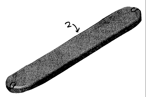
drawings. Figure 1 is an oblique, perspective view of a sensor 2, an
embodiment of the
invention. Sensor 2 preferably has an outer coating of biocompatible silicone.
[0037] Figure 2 is a top, partial cross-section of a schematic representation
of
sensor 2 where a wire spiral inductor coil 4 is positioned in planar fashion
in a substrate
6. Optionally sensor 2 may have recesses 8, each with a hole 10, to receive a
tether wire
(not shown here) for delivery of the device into a human patient, as described
below.
[0038] In the embodiment of the invention shown in Figure 3, a wire 12
connects
coil 4 to a capacitor plate 14 positioned within coil 4.
[0039] Figure 4 is a slightly oblique cross-section across its width of the
embodiment of the invention shown in Figure 2, where it can be seen that
sensor 2 is
comprised of a lower substrate 20 and an upper substrate 22. Lower substrate
20 and
upper substrate 22 are constructed from a suitable material, such as glass,
fused silica,
sapphire, quartz, or silicon. Fused silica is the preferred material of
construction. Lower
substrate 20 has on its upper surface 24 an induction coil 26, and upper
substrate 22 has a
recess 28 with a surface 30 having an induction coil 32 thereon. The top
surface of upper
substrate 22 forms a membrane 34 capable of mechanically responding to changes
in a
patient's physical property, such as pressure. The end 36 of sensor 2 has a
notch or
recess 38.
[0040] In similar fashion, Figure 5 is a slightly oblique cross-section across
its
width of the embodiment of the invention shown in Figure 3. The primary
difference
between Figures 4 and 5 is the presence of upper capacitor plate 42 and lower
capacitor
plate 44 on surfaces 24 and 30, respectively. In the embodiment of Figure 4,
the spiral
9
CA 02539261 2006-03-16
WO 2005/027998 PCT/US2004/030727
coil 4 itself acts as the capacitive element of the LC circuit that describes
the operation of
the sensor.
[0041] Figure 6 is a variation of Figure 5 where the outline of upper
substrate 22 is
shown but the details of lower substrate 20 can be seen more clearly,
including individual
coils of inductor coil 26. A wire 46 connects lower capacitor plate 44 to
induction coil
26.
[0042] The size of the sensors of the invention will vary according to factors
such
as the intended application, the delivery system, etc. The oval sensors are
intended to be
from about 0.5 in. to about 1 in. in length and from about 0.1 in. to about
0.5 in. in width,
with a thickness of from about 0.05 in. to about 0.30 in.
[0043] As shown in Figures 4 and 5, upper substrate 22 can be significantly
thinner
than lower substrate 20. By way of example, upper substrate 22 maybe from
about 100
to about 300 microns thick, whereas lower substrate 20 may be from about 500
to about
1500 microns thick. In an alternate embodiment of the invention, both
substrates may be
of the same thickness ranging from about 100 to about 1000 microns.
[0044] In the embodiment of the invention shown in Figure 7, a sensor 50 is
attached to a hollow tube 52 that has a flexible tip 54.
[0045] Figure 8 shows the sensor 50 and specific features of the tethering
system,
namely proximal holes 56 and distal holes 58 disposed in a hollow tube 52.
[0046] Figure 9 shows a tether wire 60 that is attached to sensor 50 at sensor
holes
62 and hollow tube holes 56 and 58, and a tether wire 60 is positioned
slidably within a
hollow tube 52.
CA 02539261 2006-03-16
WO 2005/027998 PCT/US2004/030727
[0047] A better appreciation of certain aspects of the invention, especially
of a
delivery system, can be obtained from Figure 10 which shows a vessel
introducer 66 and
the delivery system 68.
[0048] Further details of the delivery system are shown in Figure 11. A double
lumen tube 70 has one channel that accepts a guidewire 72 and a second channel
that
accepts the sensor tether wire. The guidewire 72 can be advanced through hub
74. A
rigid delivery capsule 78 is disposed at the far end of the delivery catheter
and flexible tip
80 is connected to the catheter via a hollow tube 81 extending through the
delivery
capsule 78. A sensor 82 is positioned inside a slot in the delivery capsule 78
proximal to
flexible tip 80.
[00491 Figure 12 shows a lateral, cross-sectional view of this arrangement
where
the sensor 82 is inside the slot of delivery capsule 78 and the flexible tip
84 of the tether
wire is disposed between the end of delivery capsule 78 and flexible tip 80.
[0050] Figure 13 shows delivery catheter 68 loaded into the previously placed
vessel introducer 66 prior to introduction of the sensor into the body.
[0051] Figure 14 shows that the sensor 82on tether tube 52 has been advanced
out
of delivery capsule 78 and the delivery catheter has been removed.
[0052] In Figure 15, the tether wire has been retracted into the hollow tether
tube,
releasing the sensor. The tether wire, tether tube and vessel introducer 66
are then all
removed.
11
CA 02539261 2010-08-16
WO 2005/027998 PCT/US2004/030727
[0053] The pressure sensor of the invention can be manufactured using Micro-
machining techniques that were developed for the integrated circuit industry.
An
example of this type of sensor features an inductive-capacitive (LC) resonant
circuit with
a variable capacitor, as is described in Allen et al., U.S. Patents Nos.
6,111,520 and
6,278,379. The sensor contains two
types of passive electrical components, namely, an inductor and a capacitor.
The sensor is
constructed so that the fluid pressure at the sensor's surface changes the
distance between
the capacitor's substantially parallel plates and causes a variation of the
sensor's
capacitance.
[0054] In a preferred embodiment the sensor of the invention is constructed
through a series of steps that use standard MEMS manufacturing techniques.
[0055] Figure 16 shows the first step of this process in which a thin layer of
metal
(Protective mask) 90 is deposited onto the top and bottom surface of a fused
silica wafer
92 (alternative materials would be glass, quartz, silicon or ceramic). Wafer
diameters can
range from about 3 to about 6 in. Wafer thickness can range from about 100 to
about
1500 microns. A pattern mask is then created on one side of the wafer to
define the
location of cavities that need to be etched into the surface.
[0056] Figure 17 shows trenches or cavities 94 are etched into one surface of
the
wafer 92 to depths ranging from about 20 to about 200 microns. This etching is
accomplished using any combination of standard wet and dry etching techniques
(acid
etch, plasma etch, reactive ion etching) that are well known in the MEMS
industry. The
protective metal mask is removed using standard metal etching techniques
[0057] In Figure 18, a thin metal seed layer 96 (typically chromium) is
deposited
on the etched side of the wafer using standard metal deposition techniques
such as
sputtering, plating or metal evaporation.
12
CA 02539261 2006-03-16
WO 2005/027998 PCT/US2004/030727
[0058] In Figure 19 a layer of photo-resistive material 98 is applied to the
etched
surface of the wafer using standard spin coating procedures.
[0059] Figure 20 shows that a mask aligner and UV light 102 is used in a
photolithographic processes to transfer a pattern from a mask 104 to the
photoresist
coating on the wafer.
[0060] In Figure 21, the non-masked portions of the Photoresist are removed
chemically creating a mold 106 of the desired coil pattern.
[0061] Figure 22 shows copper 108 electroplated into the mold to the desired
height, typically from about 5 to about 35 microns.
[0062] In Figure 23, the Photoresist 110 and seed layer 112 are etched away
leaving the plated copper coils 114.
[0063] This process is then repeated with a second wafer.
[0064] In Figure 24, the two processed wafers 118 and 120 are aligned such
that
the cavities 122 and 124 with plated coils are precisely orientated in over
one another and
temporarily bonded to each other.
[0065] Figures 25 and 26 show that by using a CO2 laser 126 (or other
appropriate
laser type), the individual sensors 130 are cut from the glass wafer. The
laser cutting
process results in a permanent, hermetic seal between the two glass wafers.
The laser
energy is confined to a precise heat effect zone 128 in which the hermetic
seal is created.
[0066] Figure 27 represents an embodiment of the invention wherein a sensor
132
attached to a delivery catheter 134 has a stabilizer or basket 136. The
stabilizer can be
any appropriate device or structure that can be fixedly attached to a sensor
of the
invention to assist the sensor in maintaining position, location, and/or
orientation after the
13
CA 02539261 2006-03-16
WO 2005/027998 PCT/US2004/030727
sensor is delivered to an intended site. The stabilizer can comprise any
appropriate
physiologically acceptable rigid or slightly flexible material, such as
stainless steel,
nitinol, or a radiopaque metal or alloy.
[00671 This sensor design provides many important benefits to sensor
performance. The hermetic seal created during the laser cutting process,
coupled with the
design feature that the conductor lines of the sensor are sealed within the
hermetic cavity,
allows the sensor to remain stable and drift free during long time exposures
to body
fluids. In the past, this has been a significant issue to the development of
sensors
designed for use in the human body. The manufacturing methodology described
above
allows many variations of sensor geometry and electrical properties. By
varying the
width of the coils, the number of turns and the gap between the upper and
lower coils the
resonant frequency that the device operates at and the pressure sensitivity
(i.e., the change
in frequency as a result of membrane deflection) can be optimized for
different
applications. In general, the design allows for a very small gap between the
coils
(typically between about 3 and about 35 microns) that in turn provides a high
degree of
sensitivity while requiring only a minute movement of the coils to sense
pressure
changes. This is important for long term durability, where large membrane
deflection
could result in mechanical fatigue of the pressure sensing element.
[00681 The thickness of the sensor used can also be varied to alter mechanical
properties. Thicker wafers are more durable for manufacturing. Thinner sensors
allow
for creating of thin pressure sensitive membranes for added sensitivity. In
order to
optimize both properties the sensors may be manufactured using wafers of
different
thicknesses. For example, one side of the sensor may be constructed from a
sensor of
approximate thickness of 200 microns. This wafer is manufactured using the
steps
outlined above. Following etching, the thickness of the pressure sensitive
membrane (i.e.,
the bottom of the etched trench) is in the range of from about 85 to about 120
microns.
14
CA 02539261 2006-03-16
WO 2005/027998 PCT/US2004/030727
The matching wafer is from about 500 to about 1000 microns thick. In this
wafer, the
trench etching step is eliminated and the coils are plated directly onto the
flat surface of
the wafer extending above the wafer surface a height of from about 20 to about
40
microns. When aligned and bonded, the appropriate gap between the top and
bottom coils
is created to allow operation preferably in a frequency range of from 30 to 45
MHz and
have sensitivity preferably in the range of from 5 to 15 kHz per millimeter of
mercury.
Due to the presence of the from about 500 to about 1000 micron thick wafer,
this sensor
will have added durability for endovascular delivery and for use within the
human body.
[0069] The sensor exhibits the electrical characteristics associated with a
standard
LC circuit. An LC circuit can be described as a closed loop with two major
elements, a
capacitor and an inductor. If a current is induced in the LC loop, the energy
in the circuit
is shared back and forth between the inductor and capacitor. The result is an
energy
oscillation that will vary at a specific frequency. This is termed the
resonant frequency of
the circuit and it can be easily calculated as its value is dependent on the
circuit's
inductance and capacitance. Therefore, a change in capacitance will cause the
frequency
to shift higher or lower depending upon the change in the value of
capacitance.
[0070] As noted above, the capacitor in the assembled pressure sensor consists
of
the two circular conductive segments separated by an air gap. If a pressure
force is
exerted on these segments it will act to move the two conductive segments
closer
together. This will have the effect of reducing the air gap between them which
will
consequently change the capacitance of the circuit. The result will be a shift
in the
circuit's resonant frequency that will be in direct proportion to the force
applied to the
sensor's surface.
[0071] Because of the presence of the inductor, it is possible to
electromagnetically
couple to the sensor and induce a current in the circuit. This allows for
wireless
communication with the sensor and the ability to operate it without the need
for an
CA 02539261 2010-08-16
WO 2005/027998 PCT/US2004/030727
internal source of energy such as a battery. Thus, if the sensor is located
within the sac of
an aortic aneurysm, it will be possible to determine the pressure within the
sac in a
simple, non-invasive procedure by remotely interrogating the sensor, recording
the
resonant frequency and converting this value to a pressure measurement. The
readout
device generates electromagnetic energy that penetrates through the body's
tissues to the
sensor's implanted location. The sensor's electrical components absorb a
fraction of the
electromagnetic energy that is generated by the readout device via inductive
coupling.
This coupling induces a current in the sensor's circuit that oscillates at the
same
frequency as the applied electromagnetic energy. Due to the nature of the
sensor's
electro-mechanical system there exists a frequency of alternating current at
which the
absorption of energy from the readout device is at a maximum. This frequency
is a
function of the capacitance of the device. Therefore, if the sensor's
capacitance changes,
so will the optimal frequency at which it absorbs energy from the readout
device. Since
the sensor's capacitance is mechanically linked to the fluid pressure at the
sensor's
surface, a measurement of this frequency by the readout device gives a
relative
measurement of the fluid pressure. If calibration of the device is performed,
then an
absolute measurement of pressure can be made. See, for example, the extensive
discussion in the Allen et al. patent, as well as
Gershenfeld et al., U.S. Patent No. 6,025,725,
Alternative readout schemes, such as phase-correlation approaches to detect
the resonant
frequency of the sensor, may also be employed.
[00721 The pressure sensor is made of completely passive components having no
active circuitry or power sources such as batteries. The pressure sensor is
completely
self-contained having no leads to connect to an external circuit or power
source.
Furthermore, these same manufacturing techniques can be used to add additional
sensing
capabilities, such as the ability to measure temperature by the addition of a
resistor to the
basic LC circuit or by utilizing changes in the back pressure of gas
intentionally sealed
16
CA 02539261 2006-03-16
WO 2005/027998 PCT/US2004/030727
within the hermetic pressure reference to change the diaphragm position and
therefore the
capacitance of the LC circuit.
[00731 It is within the scope of the invention that the frequency response to
the
sensor will be in the range of from about 1 to about 200 MHz, preferably from
about 1 to
about 100 MHz, and more preferably from about 2 to about 90 MHz, and even more
preferably from about 30 to about 45 MHz, with a Q factor of from about 5 to
about 150,
optimally from about 5 to about 80, preferably from about 40 to about 100,
more
preferably from about 50 to about 90.
[0074] In a further embodiment of the invention there is no direct conductor-
based
electrical connection between the two sides of the LC circuit. Referring again
to the
sensor described in the Allen et al. patents, the device is constructed using
multiple layers
upon lie the necessary circuit elements. Disposed on the top and bottom layer
are metal
patterns constructed using micro-machining techniques which define a top and
bottom
conductor and a spiral inductor coil. To provide for an electrical contact
between the top
and bottom layers small vias or holes are cut through the middle layers. When
the layers
are assembled, a metal paste is forced into the small vias to create direct
electrical
connections or conduits. However, experimentation has shown that due to
additional
capacitance that is created between the top and bottom inductor coils, a
vialess
operational LC circuit can be created. This absence of via holes represents a
significant
improvement to the sensor in that it simplifies the manufacturing process and,
more
importantly, significantly increases the durability of the sensor making it
more
appropriate for use inside the human body.
[00751 Further, the invention is not limited to the implantation of a single
sensor.
Multiple pressure sensors may be introduced into the aneurysm space, each
being
positioned at different locations. In this situation, each sensor may be
designed with a
unique signature (obtained by changing the resonant frequency of the sensor),
so that the
17
CA 02539261 2006-03-16
WO 2005/027998 PCT/US2004/030727
pressure measurement derived from one sensor can be localized to its specific
position
within the aneurysm.
[0076] A significant design factor that relates to the performance of the
sensor and
the operation of the system is the Quality factor (Q) associated with the
sensor. The
value of Q is one of the key determinates as to how far from the sensor the
external read-
out electronics can be located while still maintaining effective
communication. Q is
defined as a measure of the energy stored by the circuit divided by the energy
dissipated
by the circuit. Thus, the lower the loss of energy, the higher the Q.
[0077] Additional increases in Q can be achieved by removing the central
capacitive plate and using capacitive coupling between the copper coils to act
as the
capacitor element.
[0078] In operation, energy transmitted from the external read-out electronics
will
be stored in the LC circuit of the sensor. This stored energy will induce a
current in the
LC loop which will cause the energy to be shared back and forth between the
inductor
and capacitor. The result is an oscillation that will vary at the resonant
frequency of the
LC circuit. A portion of this ocscillating energy is then coupled back to the
receiving
antenna of the read-out electronics. In high Q sensors, most of the stored
energy is
available for transmission back to the electronics, which allows the distance
between the
sensor and the receiving antenna to be increased. Since the transmitted energy
will decay
exponentially as it travels away from the sensor, the lower the energy
available to be
transmitted, the faster it will decay below a signal strength that can be
detected by the
receiving antenna and the closer the sensor needs to be situated relative to
the receiving
electronics. In general then, the lower the Q, the greater the energy loss and
the shorter
the distance between sensor and receiving antenna required for sensor
detection.
18
CA 02539261 2006-03-16
WO 2005/027998 PCT/US2004/030727
[00791 The Q of the sensor will be dependent on multiple factors such as the
shape, size, diameter, number of turns, spacing between turns and cross-
sectional area of
the inductor component. In addition, Q will be greatly affected by the
materials used to
construct the sensors. Specifically, materials with low loss tangents will
provide the
sensor with higher Q factors.
[00801 The implantable sensor ascending to the invention is preferably
constructed
of various glasses or ceramics including but not limited to fused silica,
quartz, pyrex and
sintered zirconia, that provide the required biocompatibility, hermeticity and
processing
capabilities. Preferably the materials result in a high Q factor. These
materials are
considered dielectrics, that is, they are poor conductors of electricity, but
are efficient
supporters of electrostatic or electroquasiatatic fields. An important
property of dielectric
materials is their ability to support such fields while dissipating minimal
energy. The
lower the dielectric loss (the proportion of energy lost), the more effective
the dielectric
material in maintaining high Q. For a lossy dielectric material, the loss is
described by
the property termed "loss tangent." A large loss tangent reflects a high
degree of
dielectric loss.
[0081] With regard to operation within the human body, there is a second
important issue related to Q, namely, that blood and body fluids are
conductive mediums
and are thus particularly lossy. The consequence of this fact is that when a
sensor is
immersed in a conductive fluid, energy from the sensor will dissipate,
substantially
lowering the Q and reducing the sensor-to-electronics distance. For example,
the sensors
described above were immersed in saline (0.9% salt solution), and the measured
Q
decreased to approximately 10. It has been found that such loss can be
minimized by
further separation of the sensor from the conductive liquid. This can be
accomplished,
for example, by encapsulating the sensor in a suitable low-loss-tangent
dielectric
material. However, potential encapsulation material must have the flexibility
and
19
CA 02539261 2006-03-16
WO 2005/027998 PCT/US2004/030727
biocompatibility characteristics of the sensor material and also be
sufficiently compliant
to allow transmission of fluid pressure to the pressure sensitive diaphragm. A
preferred
material for this application is polydimethylsiloxane (silicone).
[0082] As an example, a thin (i.e., 200 micron) coating of silicone was
applied to
the sensor detailed above. This coating provided sufficient insulation to
maintain the Q at
50 in a conductive medium. Equally important, despite the presence of the
silicone,
adequate sensitivity to pressure changes was maintained and the sensor
retained sufficient
flexibility to be folded for endovascular delivery. One additional benefit of
the silicone
encapsulation material is that it can be optionally loaded with a low
percentage (i.e., 10 -
20%) of radio-opaque material (e.g., barium sulfate) to provide visibility
when examined
using fluoroscopic x-ray equipment. This added barium sulfate will not affect
the
mechanical and electrical properties of the silicone.
[0083] As described above, it is desirable to increase the Q factor of a
sensor, and
the Q factor can be increased by suitable selection of sensor materials or a
coating, or
both. Preferably both are used, because the resulting high Q factor of a
sensor prepared
in this fashion is especially suitable for the applications described.
[0084] When introduced into the sac of an abdominal aorta, the pressure sensor
can
provide pressure related data by use of an external measuring device. As
disclosed in the
Allen et al. patents, several different excitation systems can be used. The
readout device
generates electromagnetic energy that can penetrate through the body's tissues
to the
sensor's implanted location. The sensor's electrical components can absorb a
fraction of
the electromagnetic energy that is generated by the readout device via
inductive coupling.
This coupling will induce a current in the sensor's circuit that will
oscillate at the same
frequency as the applied electromagnetic energy. Due to the nature of the
sensor's electro-
mechanical system there will exist a frequency of alternating current at which
the
absorption of energy from the readout device is at a minimum. This frequency
is a
CA 02539261 2006-03-16
WO 2005/027998 PCT/US2004/030727
function of the capacitance of the device. Therefore, if the sensor's
capacitance changes
so will the frequency at which it minimally absorbs energy from the readout
device.
Since the sensor's capacitance is mechanically linked to the fluid pressure at
the sensor's
surface, a measurement of this frequency by the readout device can give a
relative
measurement of the fluid pressure. If calibration of the device is performed
then an
absolute measurement of pressure can be made
[0085] The circuitry used to measure and display pressure is contained within
a
simple to operate, portable electronic unit 400, as shown in Figure 28. This
unit 400 also
contains the antenna needed to perform the electromagnetic coupling to the
sensor. The
antenna may be integrated into the housing for the electronics or it may be
detachable
from the unit so that it can be positioned on the surface of the body 402 in
proximity to
the implanted sensor and easily moved to optimize the coupling between antenna
and
sensor. The antenna itself may consist of a simple standard coil configuration
or my
incorporate ferrous elements to maximize the coupling efficiency. The
electronic device
would feature an LCD or LED display 404 designed to clearly display the
recorded
pressure in physiologically relevant units such as mm Hg. In an alternative
embodiment,
the display may be created by integrating a commercially available hand-held
computing
device such as a Palm or micro-PC into the electronic circuitry and using
this device's
display unit as the visual interface between the equipment and its operator. A
further
advantage of this approach is that the hand-held computer could be detached
from the
read-out unit and linked to a standard desktop computer. The information from
the
device could thus be downloaded into any of several commercially available
data
acquisition software programs for more detailed analysis or for electronic
transfer via
hard media or the internet to a remote location.
[0086] Accordingly, the present invention provides for an impedance system and
method of determining the resonant frequency and bandwidth of a resonant
circuit within
21
CA 02539261 2006-03-16
WO 2005/027998 PCT/US2004/030727
a particular sensor. The system includes a loop antenna, which is coupled to
an
impedance analyzer. The impedance analyzer applies a constant voltage signal
to the loop
antenna scanning the frequency across a predetermined spectrum. The current
passing
through the transmitting antenna experiences a peak at the resonant frequency
of the
sensor. The resonant frequency and bandwidth are thus determined from this
peak in the
current.
[0087] The method of determining the resonant frequency and bandwidth using an
impedance approach may include the steps of transmitting an excitation signal
using a
transmitting antenna and electromagnetically coupling a sensor having a
resonant circuit
to the transmitting antenna thereby modifying the impedance of the
transmitting antenna.
Next, the step of measuring the change in impedance of the transmitting
antenna is
performed, and finally, the resonant frequency and bandwidth of the sensor
circuit are
determined.
[0088] In addition, the present invention provides for a transmit and receive
system
and method for determining the resonant frequency and bandwidth of a resonant
circuit
within a particular sensor. According to this method, an excitation signal of
white noise
or predetermined multiple frequencies is transmitted from a transmitting
antenna, the
sensor being electromagnetically coupled to the transmitting antenna. A
current is
induced in the resonant circuit of the sensor as it absorbs energy from the
transmitted
excitation signal, the current oscillating at the resonant frequency of the
resonant circuit.
A receiving antenna, also electromagnetically coupled to the transmitting
antenna,
receives the excitation signal minus the energy which was absorbed by the
sensor. Thus,
the power of the received signal experiences a dip or notch at the resonant
frequency of
the sensor. The resonant frequency and bandwidth are determined from this
notch in the
power.
22
CA 02539261 2006-03-16
WO 2005/027998 PCT/US2004/030727
[0089] The transmit and receive method of determining the resonant frequency
and
bandwidth of a sensor circuit includes the steps of transmitting a multiple
frequency
signal from transmitting antenna, and, electromagnetically coupling a resonant
circuit on
a sensor to the transmitting antenna thereby inducing a current in the sensor
circuit. Next,
the step of receiving a modified transmitted signal due to the induction of
current in the
sensor circuit is performed. Finally, the step of determining the resonant
frequency and
bandwidth from the received signal is executed.
[0090] Yet another system and method for determining the resonant frequency
and
bandwidth of a resonant circuit within a particular sensor includes a chirp
interrogation
system. This system provides for a transmitting antenna which is
electromagnetically
coupled to the resonant circuit of the sensor. An excitation signal of white
noise or
predetermined multiple frequencies, or a time-gated single frequency is
applied to the
transmitting antenna for a predetermined period of time, thereby inducing a
current in the
resonant circuit of the sensor at the resonant frequency. The system then
listens for a
return signal which is coupled back from the sensor. The resonant frequency
and
bandwidth of the resonant circuit are determined from the return signal.
[0091] The chirp interrogation method for determining the resonant frequency
and
bandwidth of a resonant circuit within a particular sensor includes the steps
of
transmitting a multi-frequency signal pulse from a transmitting antenna,
electromagnetically coupling a resonant circuit on a sensor to the
transmitting antenna
thereby inducing a current in the sensor circuit, listening for and receiving
a return signal
radiated from the sensor circuit, and determining the resonant frequency and
bandwidth
from the return signal.
[0092] The present invention also provides an analog system and method for
determining the resonant frequency of a resonant circuit within a particular
sensor. The
analog system comprises a transmitting antenna coupled as part of a tank
circuit which in
23
CA 02539261 2006-03-16
WO 2005/027998 PCT/US2004/030727
turn is coupled to an oscillator. A signal is generated which oscillates at a
frequency
determined by the electrical characteristics of the tank circuit. The
frequency of this
signal is further modified by the electromagnetic coupling of the resonant
circuit of a
sensor. This signal is applied to a frequency discriminator which in turn
provides a signal
from which the resonant frequency of the sensor circuit is determined.
[0093] The analog method for determining the resonant frequency and bandwidth
of a resonant circuit within a particular sensor includes the steps of
generating a
transmission signal using a tank circuit which includes a transmitting
antenna, modifying
the frequency of the transmission signal by electromagnetically coupling the
resonant
circuit of a sensor to the transmitting antenna, and converting the modified
transmission
signal into a standard signal for further application.
[0094] The invention further includes an alternative method of measuring
pressure
in which a non-linear element such as a diode or polyvinylidenedifloride piezo-
electric
polymer is added to the LC circuit. A diode with a low turn-on voltage such as
a
Schottky diode can be fabricated using micro-machining techniques. The
presence of this
non-linear element in various configurations within the LC circuit can be used
to
modulate the incoming signal from the receiving device and produce different
harmonics
of the original signal. The read-out circuitry can be tuned to receive the
particular
harmonic frequency that is produced and use this signal to reconstruct the
fundamental
frequency of the sensor. The advantage of this approach is two-fold; the
incoming signal
can be transmitted continuously and since the return signal will be at
different signals, the
return signal can also be received continuously.
[0095] The above methods lend themselves to the creation of small and simple
to
manufacture hand-held electronic devices that can be used without
complication.
24
CA 02539261 2006-03-16
WO 2005/027998 PCT/US2004/030727
[0096] The preceding specific embodiments are illustrative of the practice of
the
invention. It is to be understood, however, that other expedients known to
those skilled
in the art or disclosed herein, may be employed without departing from the
spirit of the
invention of the scope of the appended claims.