Note: Descriptions are shown in the official language in which they were submitted.
CA 02540968 2006-03-27
1
PHOTOVOLTAIC ULTRAVIOLET SENSOR
BACKGROUND OF THE INVENTION:
[0001] This invention relates to a photovoltaic uftraviolet sensor comprising
a zinc
oxide single crystal.
[0002] JP-A H03-241777, which is incorporated herein by reference in its
entirety,
discloses a photoconductive ultraviolet sensor which comprises a substrate and
a zinc
oxide thin film formed on the substrate. In JP-A H03-241777, the zinc oxide
thin film
preferably has an optical forbidden band of about 3.0 to about 3.2 eV.
However, the
zinc oxide thin film of the foregoing optical forbidden band is sensitive also
to visible
rays and therefore has insufficient sensitivity to ultraviolet rays.
[00031 JP-A H10-182290, which is incorporated herein by reference in its
entirety,
discloses another ultraviolet sensor which comprises a zinc oxide crystal
whose "a"
face is used as an ultraviolet receiver surface. To sense ultraviolet rays,
impedance
variation of the zinc oxide crystal is monitored while the zinc oxide crystal
is supplied
with electric fields according to an antiresonance frequency of the zinc oxide
crystal.
However, generation of the antiresonance frequency requires special equipment
so
that the total cost of the ultraviolet sensor becomes high. In addition, the
ultraviolet
sensor of JP-A H10-182290 has a relatively slow response because of its
sensing
mechanism.
SUMMARY OF THE INVENTION:
[0004] It is an object of the present invention to provide an ultraviolet
sensor which is
not sensitive to visible rays and has a relatively fast response without using
complex
equipment.
[0005] According to one aspect of the present invention, a photovoltaic
ultraviolet
sensor comprises a zinc oxide single crystal and an ultraviolet receiver. The
zinc oxide
CA 02540968 2006-03-27
2
single crystal has a +c face. The ultraviolet receiver is formed on the +c
face of the
zinc oxide single crystal and, when receiving ultraviolet rays, produces a
voltage
solely or in cooperation with the zinc oxide single crystal.
[0006] An appreciation of the objectives of the present invention and a more
complete understanding of its structure may be had by studying the following
description of the preferred embodiment and by referring to the accompanying
drawings.
BRIEF DESCRIPTION OF THE DRAWINGS:
[0007] Fig. 1 is a partially-sectional, perspective view showing a
photovoltaic
ultraviolet sensor according to a first embodiment of the present invention;
[0008] Fig. 2 is a generally schematic view showing a zinc oxide single
crystal block;
[0009] Fig. 3 is a generally schematic view showing a crystal structure of a
zinc oxide
single crystal;
[0010] Fig. 4 is a sectional view showing a fabrication process for the
photovoltaic
ultraviolet sensor of Fig. 1;
[0011] Fig. 5 is a sectional view showing a subsequent fabrication process for
the
photovoltaic ultraviolet sensor of Fig. 1;
[0012] Fig. 6 is a sectional view showing a subsequent fabrication process for
the
photovoltaic ultraviolet sensor of Fig, 1;
[0013] Fig. 7 is a sectional view showing a subsequent fabrication process for
the
photovoltaic ultraviolet sensor of Fig. 1;
[0014] Fig. 8 is a sectional view showing a subsequent fabrication process for
the
photovoltaic ultraviolet sensor of Fig. 1;
[0015] Fig. 9 is a sectional view showing a subsequent fabrication process for
the
photovoltaic ultraviolet sensor of Fig, 1;
[0016] Fig. 10 is a sectional view showing a subsequent fabrication process
for the
CA 02540968 2006-03-27
3
photovoltaic ultraviolet sensor of Fig. 1;
[0017] Fig. 11 is a view showing a sensing characteristic of the photovoitaic
ultraviolet sensor of Fig. 1;
[0018] Fig. 12 is a partially-sectional, perspective view showing a
photovoltaic
ultraviolet sensor according to a second embodiment of the present invention;
[0019] Fig. 13 is a sectional view showing a fabrication process for the
photovoltaic
ultraviolet sensor of Fig. 12;
[0020] Fig. 14 is a sectional view showing a subsequent fabrication process
for the
photovoltaic ultraviolet sensor of Fig. 12;
[0021] Fig. 15 is a sectional view showing a subsequent fabrication process
for the
photovoltaic ultraviolet sensor of Fig. 12;
[0022] Fig. 16 is a sectional view showing a subsequent fabrication process
for the
photovoltaic ultraviolet sensor of Fig, 12;
[0023] Fig. 17 is a sectional view showing a subsequent fabrication process
for the
photovoltaic ultraviolet sensor of Fig. 12;
[0024) Fig. 18 is a sectional view showing a subsequent fabrication process
for the
photovoltaic ultraviolet sensor of Fig. 12;
[0025] Fig. 19 is a sectional view showing a subsequent fabrication process
for the
photovoltaic ultraviolet sensor of Fig. 12;
[0026] Fig. 20 is a sectional view showing a fabrication process for a
photovoltaic
ultraviolet sensor according to a third embodiment of the present invention;
100271 Fig. 21 is a sectional view showing a subsequent fabrication process
for the
photovoltaic ultraviolet sensor of Fig. 20;
[0028] Fig_ 22 is a sectional view showing a subsequent fabrication process
for the
photovoltaic ultraviolet sensor of Fig. 20;
[0029] Fig. 23 is a sectional view showing a subsequent fabrication process
for the
photovoltaic ultraviolet sensor of Fig. 20;
CA 02540968 2006-03-27
4
[0030] Fig. 24 is a sectional view showing a subsequent fabrication process
for the
photovoltaic ultraviolet sensor of Fig. 20;
[0031] Fig. 25 is a sectional view showing a subsequent fabrication process
for the
photovoltaic ultraviolet sensor of Fig. 20;
[0032] Fig. 26 is a sectional view showing a fabrication process for a
photovoltaic
ultraviolet sensor according to a fourth embodiment of the present invention;
[0033] Fig. 27 is a sectional view showing a subsequent fabrication process
for the
photovoltaic ultraviolet sensor of Fig. 26;
[00341 Fig. 28 is a sectional view showing a subsequent fabrication process
for the
photovoltaic ultraviolet sensor of Fig. 26;
[0035] Fig. 29 is a sectional view showing a subsequent fabrication process
for the
photovoltaic ultraviolet sensor of Fig. 26;
[0036] Fig. 30 is a sectional view showing a subsequent fabrication process
for the
photovoltaic ultraviolet sensor of Fig. 26;
[0037] Fig. 31 is a sectional view showing a subsequent fabrication process
for the
photovoltaic ultraviolet sensor of Fig. 26;
[0038] Fig. 32 is a sectional view showing a fabrication process for a
photovoltaic
ultraviolet sensor according to a fifth embodiment of the present invention;
[0039] Fig. 33 is a sectional view showing a subsequent fabrication process
for the
photovoltaic ultraviolet sensor of Fig. 32;
[0040j Fig. 34 is a sectional view showing a subsequent fabrication process
for the
photovoltaic ultraviolet sensor of Fig. 32;
[0041] Fig. 35 is a sectional view showing a subsequent fabrication process
for the
photovoltaic ultraviolet sensor of Fig. 32;
[0042] Fig. 36 is a sectional view showing a subsequent fabrication process
for the
photovoltaic ultraviolet sensor of Fig. 32; and
[0043] Fig. 37 is a sectional view showing a subsequent fabrication process
for the
CA 02540968 2006-03-27
photovoltaic ultraviolet sensor of Fig. 32.
DESCRIPTION OF PREFERRED EMBODIMENTS:
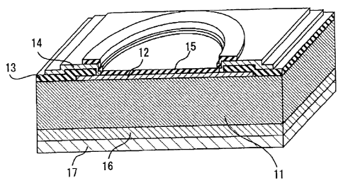
(0044] With reference to Fig. 1, a photovoftaic ultraviolet sensor according
to a first
5 embodiment of the present invention comprises a zinc oxide single crystal
substrate
11 as a main component. The zinc oxide single crystal substrate 11 is one
obtainable
by cutting a zinc oxide single crysta(1 as shown in Fig. 2 along with a plane
perpendicular to its c axis 3 so as to form a plurality of wafers 2, followed
by carrying
out a heat treatment for one of the wafers 2 under an oxygen-containing
atmosphere
within a container made of high-purity zinc oxide. Thus, the heat-treated
wafer 2 can
be obtained, which includes a plurality of zinc oxide single crystal
substrates 11. After
a plurality of photovoltaic ultraviolet sensors are formed on the heat-treated
wafer 2,
the wafer 2 is diced so that the plurality of photovoltaic ultraviolet
sensors, i.e_ the zinc
oxide single crystal substrates 11 are obtained together with predetermined
components described hereinafter in detail.
(0045] As apparent from the above description, the zinc oxide single crystal
substrate
11 has two surfaces which are +c face and -c face of the zinc oxide single
crystal. In
detail, as shown in Fig. 3, the -c face 5 of the zinc oxide single crystal is
a face defined
by four oxygen atoms and is also referred to as "O-face," while the +c face 6
of the
zinc oxide single crystal is a face defined by four zinc atoms and is also
referred to as
"Zn-face. Another face 4 perpendicular to the -c face 5 and +c face 6 is
referred to as
"a" face. In addition, the zinc oxide single crystal as shown in Fig. 2 is
formed in
accordance with the hydrothermal synthesis method using LiOH or KOH as a
mineralizer. The zinc oxide single crystal may be formed in accordance with
another
method, for example, vapor deposition method, flux method, scorification
method,
molecular beam epitaxy (MBE) method, vacuum deposition method, metal organic
chemical vapor deposition (MOCVD) method, or spattering method.
CA 02540968 2006-03-27
6
[0046) Turning back to Fig. 1, the photovoltaic ultraviolet sensor of the
present
embodiment further comprises an ultraviolet receiver formed on the +c face of
the zinc
oxide single crystal substrate 11. The ultra violet receiver of the present
embodiment
is a Schottky electrode 12 formed directly on the +c face of the zinc oxide
single
crystal substrate 11, for example, under an oxygen atmosphere. The Schottky
electrode 12 serves as an ultraviolet receiver surface and, when receiving
ultraviolet
rays, produces a voltage in cooperation with the zinc oxide single crystal
substrate 11.
The Schottky electrode 12 may comprise one or more layers, each of which is
made
of Pt, Ru, Pd, Au, Ni, Ir, Os, Re, Rh, Te or W. The Schottky electrode 12 of
the present
embodiment has a predetermined thickness such that the Schottky electrode 12
is
ultraviolet-permeable. Instead, the Schottky electrode 12 may have another
thickness
thicker than the predetermined thickness, provided that the Schottky electrode
12 has
a special shape such as a comb-like such that ultraviolet rays are allowed to
reach the
Schottky junction between the Schottky electrode 12 and the +c face 6 of the
zinc
oxide single crystal.
[0047] As shown in Fig. 1, the photovoltaic ultraviolet sensor of the present
embodiment further comprises a passivation film 13, an additional electrode
14, an
antireflection film 15, an AZO(Al-doped Zinc Oxide) thin film 16 and an ohmic
electrode 17.
[0048] The passivation film 13 is made of one or more insulator materials and
covers
a peripheral region on the +c face of the zinc oxide single crystal substrate
11 and a
peripheral part of the Schottky electrode 12. The passivation film 13 may
comprise at
least a layer made of AI203, Si02, SiNO, SiN, AIN, SIALON(siiicon aluminum
oxynitride), ZnS or ZnO.
[0049] The additional electrode 14 is electrically connected to the Schottky
electrode
12 and is formed on the passivation film 13 so that the Schottky electrode 12
is
electrically accessible from the outside through the additional electrode 14.
The
CA 02540968 2006-03-27
7
additional electrode 14 may comprise one or more layers, each of which is made
of Pt,
Ru, Pd, Au, or Ni.
[0050] The'antireflection film 15 is'formed on a receiving portion of the
ultraviolet
receiver, i.e. a center region of the Schottky electrode 12 as shown in Fig.
1. The
antireflection film 15 has a thickness of 1 to 200 nm and is ultraviolet-
permeable. The
antireflection film comprises one or more layers, each of which is made of
A1203, Si02,
SiNO, SiN, ZnS or ZnO.
['0051] The AZO thin film 16 is formed on the -c face of the zinc oxide single
crystal
substrate 11, and the ohmic electrode 17 is formed on the AZO thin film 16.
The ohmic
electrode 17 may comprise one or more layers, each of which is made of Al, Cr,
Zn, Ti,
Ru, Pd, Pt, Ni, In, Au, Cu or W.
[0052] Now, an explanation will be made about fabrication processes for the
exemplary photovoltaic ultraviolet sensor according to the present embodiment,
with
reference to Figs. 4 to 10.
[0053] First, the heat-treated wafer 2 including the zinc oxide single crystal
substrates 11 is prepared in a manner as described above. However, Fig. 4
shows
only one zinc oxide single crystal substrate 11, for the sake of clarity. For
the same
reason, Figs. 5 to 10 are illustrated in connection with only one zinc oxide
single
crystal substrate 11. The illustrated zinc oxide single crystal substrate 11
has +c face
as an upper surface and -c face as a lower surface.
[0054] Next, as shown in Fig_ 5, the Schottky electrode 12 is formed, for
example, by
forming a first resist pattern on the upper surface of the zinc oxide single
crystal
substrate 11 by means of the photolithography technique, followed by forming a
Pt
thin film of 3 nm by means of the sputtering method, further followed by
lifting off the
first resist pattem together with the Pt thin film formed thereon.
[0055] Next, as shown in Fig. 6, the passivation film 13 is formed, for
example, by
forming a second resist pattem only covering the center area of the Schottky
CA 02540968 2006-03-27
8
electrode 12, followed by forming a Si02 thin film of 200 nm by means of the
sputtering method, further followed by lifting off the second resist pattem
together with
the Si02 thin film formed thereon. After the formation of the passivation film
13, the
thus obtained intermediate product is subjected to a heat treatment process.
[0056] Next, as shown in Fig. 7, the additional electrode 14 is formed, for
example,
by forming a third resist pattern, followed by forming a Pt thin film of 300
nm by means
of the sputtering method, further followed by lifting off the third resist
pattern together
with the Pt thin film formed thereon, wherein the third resist pattern has two
parts, one
of which is a center pattern smaller than the second resist pattern and
deposited on
the center area of the Schottky electrode 12, the other one is a peripheral
pattern
having a first width and positioned on the peripheral portion of the
passivation film 13.
[0057] Next, as shown in Fig. 8, the antireflection film 15 is formed, for
example, by
forming a fourth resist pattern on the peripheral portion of the thus obtained
intermediate product, followed by forming a Si02 thin film of 60 nm by means
of the
sputtering method, further followed by lifting off the fourth resist pattern
together with
the Si02 thin film formed thereon, wherein the fourth resist pattern has a
second width
wider than the first width of the third resist pattern. After the formation of
the
antireflection film 15, the thus obtained intermediate product is subjected to
a heat
treatment process.
[0058] Next, as shown in Fig. 9, the AZO thin film 16 is formed on the lower
surface
of the zinc oxide single crystal substrate 11, for example, by the sputtering
method,
wherein the exemplary AZO thin film 16 has a thickness of 100 nm.
[0059] Next, as shown in Fig, 10, an Al thin film of 300 nm is formed as the
ohmic
electrode 17 on the AZO thin film 16, for example, by the sputtering method.
After that,
as mentioned above, the wafer is diced into the ultraviolet sensor chips, each
of which
has a size of 1 mm (H) x 1 mm (W) x 0.3 mm (T).
[0060] The thus obtained ultraviolet sensor according to the present
embodiment has
CA 02540968 2006-03-27
9
an ultraviolet sensing characteristic shown in Fig. 11. The measured bandwidth
is
from 250 nm to 600 nm, while the response bandwidth is from 250 nm to 380 nm.
As
understood from the illustrated characteristic, the ultraviolet sensor of the
present
embodiment is usable for sensing UV A(ultraviolet A) of 320 to 400 nm, UV-B
(ultraviolet B) of 280 to 320 nm, and UV-C (ultraviolet C) of 280 nm or
smaller. The
illustrated characteristic further shows that the exemplary ultraviolet sensor
has a
sensitivity peak on approximately 350 nm but does not have any sensitivity to
the
visible- rays. In addition, the exemplary ultraviolet sensor has a relatively
fast response
of several microseconds.
[0061] Next explanation will be made about a photovoltaic ultraviolet sensor
according to a second embodiment of the present invention, with reference to
Fig. 12.
The ultraviolet sensor of the present embodiment is a modification of the
ultraviolet
sensor of the first embodiment. In this connection, like numerals are used to
denote
like elements in Figs. 1 and 12. Comparing Figs. 1 and 12, the ultraviolet
sensor of the
present embodiment has a structure similar to that of the first embodiment
except that
the passivation film 13 is formed under the peripheral part of the Schottky
electrode
12.
[0062] The ultraviolet sensor of the present embodiment can be obtained in the
following manner described hereinafter with reference to Figs. 13 to 19.
[0063] First, the heat-treated wafer including the zinc oxide single crystal
substrates
11 is prepared as shown in Fig. 13. The illustrated zinc oxide single crystal
substrate
11 has +c face as an upper surface and -c face as a lower surface.
[0064] Next, as shown in Fig. 14, the passivation film 13 is formed, for
example, by
forming an A1203 thin film of 200 nm by means of the sputtering method on the
upper
surface of the zinc oxide single crystal substrate 11, followed by forming a
first resist
pattem on the peripheral portion of the AI203 thin film, further followed by
etching the
A1203 thin film by the use of the first resist pattern as a mask. After the
formation of the
CA 02540968 2006-03-27
passivation film 13, the thus obtained intermediate product is subjected to a
heat
treatment process.
[0065] Next, as shown in Fig. 15, the Schottky electrode 12 is formed, for
example,
by forming a Pt thin film of 3 nm on a region including an exposed portion of
the upper
5 surface of the zinc oxide single crystal substrate 11 by means of the
sputtering
method and photolithography techniques.
[0066] Next, as shown in Fig. 16, the additional electrode 14 is formed, for
example,
by forming a second resist pattern, followed by forming a Pt thin film of 300
nm by
means of the sputtering method, further followed by lifting off the second
resist pattern
10 together with the Pt thin film formed thereon, wherein the second resist
pattem has
two parts, one of which is a center pattern deposited on the center area of
the
Schottky electrode 12, the other one is a peripheral pattern having a first
width and
positioned on the peripheral portion of the passivation film 13.
[0067] Next, as shown in Fig. 17, the antireflection film 15 is formed, for
example, by
forming a third resist pattern on the peripheral portion of the thus obtained
intermediate product, followed by forming a Si02 thin film of 60 nm by means
of the
sputtering method, further followed by lifting off the third resist pattern
together with
the Si02 thin film formed thereon, wherein the third resist pattern has a
second width
wider than the first width of the second resist pattem. After the formation of
the
antireflection film 15, the thus obtained intermediate product is subjected to
a heat
treatment process.
[0068] Next, as shown in Fig. 18, the AZO thin film 16 is formed on the lower
surface
of the zinc oxide single crystal substrate 11, for example, by the sputfering
method,
wherein the exemplaryAZO thin film 16 has a thickness of 100 nm.
[0069] Next, as shown in Fig. 19, an Al thin film of 300 nm is formed as the
ohmic
electrode 17 on the AZO thin film 16, for example, by the sputtering method.
After that,
as mentioned above, the wafer is diced into the ultraviolet sensor chips, each
of which
CA 02540968 2006-03-27
11
has a size of 1 mm (H) x 1 mm (W) x 0.3 mm (T).
[0070] Next explanation will be made about a photovoltaic ultraviolet sensor
according to a third embodiment of the present invention, with reference to
Figs_ 20 to
25. The ultraviolet sensor of the present embodiment is a modification of the
ultraviolet sensor of the first embodiment. In this connection, like numerals
are used to
denote like elements in Figs. 1 and 20 to 25.
[0071] Comparing Figs. 1 and 25, the ultraviolet sensor of the present
embodiment
has a structure similar to that of the first embodiment except for two points.
One point
is that an adjustment thin film 18 is interposed between the zinc oxide single
crystal
substrate 11 and the Schottky electrode 12. The other point is that the
ultraviolet
sensor of the present embodiment neither has the passivation film 13 nor the
antireflection film 15. However, the passivation film 13 and/or the
antireflection film 15
may be included in a manner similar to the first or the second embodiment.
[0072] The adjustment thin film 18 is a thin film whose resistivity,
conduction type, i.e.
n- or p- type, and/or band gap are adjusted by adding at least one kind
additive into a
base material. The adjustment thin film 18 of the present embodiment comprises
a
zinc oxide based thin film. In addition, the adjustment thin film 18 of the
zinc oxide
based thin film may comprise at least one layer which is a chemical compound
selected from the group consisting of Ca, Mg, S, Al, Cd, Se, Ga, N, Cu and Te.
[0073] The ultraviolet sensor of the present embodiment can be obtained in the
following manner described hereinafter with reference to Figs. 20 to 25.
[0074] First, the heat-treated wafer including the zinc oxide single crystal
substrates
11 is prepared as shown in Fig, 20. The illustrated zinc oxide single crystal
substrate
11 has +c face as an upper surface and -c face as a lower surface.
[0075] Next, as shown in Fig. 21, the adjustment thin film 18 is formed over
the +c
face of the zinc oxide single crystal substrate 11, for example, by the MOCVD
method,
wherein the adjustment thin film 18 is an epitaxial layered zinc oxide based
thin film
CA 02540968 2006-03-27
12
into which Al is added as an additive. The exemplary adjustment thin film 18
has
resistivity of 100 to 500 II cm and is of n-type.
[0076] Next, as shown in Fig. 22, the Schottky eiectrode 12 is formed on the
adjustment thin film 18, for example, by forming a Pt thin film of 3 nm by
means of the
sputtering method. The Schottky electrode 12 and the adjustment thin film 18
constitute a Schottky barrier and, when the Schottky electrode 12 receives
ultraviolet
rays, produce a voltage.
[0077] Next, as shown in Fig. 23, the additional electrode 14 is formed, for
example,
by forming a predetermined resist pattern, followed by forming a Pt thin film
of 300 nm
by means of the sputtering method, further followed by lifting off the
predetermined
resist pattern together with the Pt thin film formed thereon.
[0078] Next, as shown in Fig. 24, the AZO thin film 16 is formed on the -c
face of the
zinc oxide single crystal substrate 11, for example, by the sputtering method,
wherein
the exemplary AZO thin film 16 has a thickness of 100 nm.
[0079] Next, as shown in Fig. 25, an Al thin film of 300 nm is formed as the
ohmic
electrode 17 on the AZO thin film 16, for example, by the sputtering method.
After that,
as mentioned above, the wafer is diced into the ultraviolet sensor chips, each
of which
has a size of 1 mm (H) x 1 mm (W) x 0.3 mm (T).
[0080] Next explanation will be made about a photovoltaic ultraviolet sensor
according to a fourth embodiment of the present invention, with reference to
Figs. 26
to 31. The photovoltaic ultraviolet sensor according to the present embodiment
has
not a Schottky junction but a p-n junction, different from the first to the
third
embodiments. However, because there are similar elements, for example, in
Figs. 1
and 26 to 31, like numerals are used to denote like elements.
[0081] The zinc oxide single crystal substrate 11 of the present embodiment is
of
n-type. On the zinc oxide single crystal substrate 11, a p-type thin film 19
is formed.
The p-type thin film 19 may comprise a p-type zinc oxide thin film, a p-type
zinc oxide
CA 02540968 2006-03-27
13
based thin film, or a p-type nitride thin film such as p-type GaN thin film.
In addition,
the p-type thin film 19 of the zinc oxide based thin film may comprise at
least one layer
which is a chemical compound selected from the group consisting of Ca, Mg, S,
Al, Cd,
Se, Ga, N, Cu and Te. On the other hand, the p-type thin film 19 of the
nitride thin film
may comprise at least one layer which is a chemical compound selected from the
group consisting of Ga, Al and In.
[0082) The ultraviolet sensor of the present embodiment can be obtained in the
following manner described hereinafter with reference to Figs. 26 to 31.
[0083] First, the heat-treated wafer including the n-type zinc oxide single
crystal
substrates 11 is prepared as shown in Fig. 26. The illustrated zinc oxide
single crystal
substrate 11 has +c face as an upper surface and -c face as a lower surface.
[0084] Next, as shown in Fig. 27, the p-type thin film 19 is formed directly
on the +c
face of the zinc oxide single crystal substrate 11, for example, by the MOCVD
method,
wherein the p-type thin film 19 is an epitaxial layered zinc oxide thin film
or a GaN thin
film.
[0085] Next, as shown in Fig. 28, the passivation film 13 is formed, for
example, by
forming an A1203 thin film of 200 nm by means of the sputtering method over
the upper
surface of the zinc oxide single crystal substrate 11 and the p-type thin film
19,
followed by forming a first resist pattern on the A1203 thin film, further
followed by
etching the A1203 thin film by the use of the first resist pattern as a mask.
The etching
process provides. the passivation film 13 with a centered large aperture and a
contact
hole which has an annular shape. After the formation of the passivation film
13, the
thus obtained intermediate product is subjected to a heat treatment process.
[0086] Next, as shown in Fig, 29, a first ohmic electrode 54 is formed, for
example,
by forming a second resist pattern, followed by forming a Ni thin film of 100
nm by
means of the sputtering method, further followed by forming an Au thin film of
200 nm
by means of the sputtering method, further followed by lifting off the
predetermined
CA 02540968 2006-03-27
14
resist pattern together with the Ni thin film and the Au thin film formed
thereon.
[0087] Next, as shown in Fig. 30, the AZO thin film 16 is formed on the -c
face of the
zinc oxide single crystal substrate 11, for example, by the sputtering method,
wherein
the exemplary AZO thin film 16 has a thickness of 100 nm.
10088] Next, as shown in Fig. 31, an Al thin film of 300 nm is formed as a
second
ohmic electrode 17 on the AZO thin film 16, for example, by the sputtering
method.
After that, as mentioned above, the wafer is diced into the ultraviolet sensor
chips,
each of which has a size of 1 mm (H) x 1 mm (W) x 0.3 mm (T).
[0089] Although the ultraviolet sensor of the present embodiment does not have
an
antireflection film, an antireflection film may be formed in a manner similar
to the first
or the second embodiment.
[0090] Next explanation will be made about a photovoltaic ultraviolet sensor
according to a fifth embodiment of the present invention, with reference to
Figs. 32 to
37. The ultraviolet sensor of the present embodiment is a modification of the
uftraviolet sensor of the third embodiment. In this connection, like numerals
are used
to denote like elements in Figs. 20 to 25 and 32 to 37. The ultraviolet sensor
of the
present embodiment has a structure similar to that of the third embodiment
except
that the adjustment thin film 21 is made not of a zinc oxide based thin film
but of a
nitride thin film interposed between the zinc oxide single crystal substrate
11 and the
Schottky electrode 12. The adjustment thin film 21 of the nitride thin film
may
comprise at least one layer which is a chemical compound selected from the
group
consisting of Ga, Al and In.
[0091] The ultraviolet sensor of the present embodiment can be obtained in the
following manner described hereinafter with reference to Figs. 32 to 37.
[0092] First, the heat-treated wafer including the zinc oxide single crystal
substrates
11 is prepared as shown in Fig. 32, The illustrated zinc oxide single crystal
substrate
11 has +c face as an upper surface and -c face as a lower surface,
CA 02540968 2006-03-27
100931 Next, as shown in Fig. 33, the adjustment thin film 21 is formed over
the +c
face'of the zinc oxide single crystal substrate 11, for example, by the MOCVD
method,
wherein the adjustment thin film 21 is an epitaxial layered n-type GaN. The
exemplary
adjustment thin film 21 has a thickness of I Nm_
5 [0094] Next, as shown in Fig. 34, the Schottky electrode 12 is formed on the
adjustment thin film 21, for example, by forming a Pt thin film of 3 nm by
means of the
sputtering method. The Schottky electrode 12 and the adjustment thin film 21
constitute a Schottky barrier and, when the Schottky electrode 12 receives
ultraviolet
rays, produce a voltage.
10 [0095] Next, as shown in Fig. 35, the additional electrode 14 is formed,
for example,
by forming a predetermined resist pattern, followed by forming a Pt thin film
of 300 nm
by means of the sputtering method, further followed by lifting off the
predetermined
resist pattern together with the Pt thin film formed thereon.
[0096] Next, as shown in Fig. 36, the AZO thin film 16 is formed on the -c
face of the
15 zinc oxide single crystal substrate 11, for example, by the sputtering
method, wherein
the exemplary AZO thin film 16 has a thickness of 100 nm.
[0097] Next, as shown in Fig. 37, an Al thin film of 300 nm is formed as the
ohmic
electrode 17 on the AZO thin film 16, for example, by the sputtering method.
After that,
as mentioned above, the wafer is diced into the ultraviolet sensor chips, each
of which
has a size of 1 mm (H) x 1 mm (VV) x 0.3 mm (T).
[0098] Although the ultraviolet sensor of the present embodiment neither has a
passivation film nor an antireflection film, a passivation film and/or an
antireflection
film may be formed in a manner similar to the first or the second embodiment.
[0099] The preferred embodiments of the present invention will be better
understood
by those skilled in the art by reference to the above description and figures.
The
description and preferred embodiments of this invention illustrated in the
figures are
not to intend to be exhaustive or to limit the invention to the precise form
disclosed.
CA 02540968 2006-03-27
16
They are chosen to describe or to best explain the principles of the invention
and its
applicable and practical use to thereby enable others skilled in the art to
best utilize
the invention.
10100] While there has been described what is believed to be the preferred
embodiment of the invention, those skilled in the art will recognize that
other and
further modifications may be made thereto without departing from the sprit of
the
invention, and it is intended to claim all such embodiments that fall within
the true
scope of the invention.