Note: Descriptions are shown in the official language in which they were submitted.
CA 02559219 2006-09-08
WO 2005/096372 PCT/EP2005/051319
1
Description
METHOD FOR FABRICATING STRAINED SILICON-
ON-INSULATOR STRUCTURES AND STRAINED SILICON-
ON-INSULATOR STRUCTURES FORMED THEREBY
Technical Field
[001] The invention relates generally to semiconductor structures and devices
and to a
method for their fabrication and, more particularly, to fabrication methods
and silicon-
on-insulator (SOI) structures, devices and integrated circuits characterized
by enhanced
carrier mobility.
Background Art
[002] Silicon-on-insulator (SOI) structures are constituted by a thin active
silicon layer
overlying a silicon dioxide insulating layer (i.e., the buried oxide, or
"BOX"), which
itself overlies a supporting silicon substrate. The advantages of SOI
structures for
metal-oxide-semiconductor field effect transistor (MOSFET) technology and com-
plimentary metal-oxide-semiconductor (CMOS) integrated circuits are well
documented. The insulating layer of the SOI structure enables field effect
transistors
(FET's) to operate at significantly higher speeds with improved electrical
isolation and
reduced electrical losses as compared with conventional bulk silicon
technologies. The
result is an increase in performance and a reduction in power consumption.
[003] In conventional MOSFET and CMOS technologies, field effect transistors
fabricated on an SOI structure include a channel formed in the active silicon
layer.
Carrier mobility is an important parameter because of its direct influence on
output
current and switching performance of the field effect transistors.
Accordingly, one
approach for increasing device performance is to enhance the channel mobility
by
straining the active silicon layer either biaxially or uniaxially. A net
strain may be
provided by introducing compressive stress into the silicon active layer or by
in-
troducing tensile stress into the silicon active layer. Straining the crystal
lattice in the
plane of the silicon layer either locally or globally alters the electronic
band structure
of the silicon layer. As a result, in-plane carrier mobility may be increased
by ten to
twenty-five percent, which results in improved device performance.
[004] Biaxial tensile strain may also be induced in a silicon layer uniformly
across an
entire substrate by introducing an intervening layer formed of a material
having a
lattice constant greater than that of silicon. For example, a biaxially
strained active
silicon layer may be produced in an SOI structure by introducing a thin
composite
layer of graded silicon germanium buffer layer and a relaxed silicon germanium
layer
between the buried oxide layer and the silicon active layer, which is
deposited
CA 02559219 2006-09-08
WO 2005/096372 PCT/EP2005/051319
2
epitaxially on the relaxed silicon germanium layer. The tensile strain
increases the in-
teratomic spacing of the silicon in the plane of the substrate, which
increases electron
mobility. A layer transfer approach may remove the silicon germanium layer.
The
existence of the uniform tensile stress enhances electron mobility in device
channels of
n-channel field effect transistors (NFET's) and hole mobility in p-channel
field effect
transistors (PFET's) for tensile stress introduced perpendicular to the
direction of
carrier flow in the PFET device channel.
[005] Uniaxial compressive strain may be induced locally in a silicon layer by
process op-
timizations. Small amounts of stress may be introduced by manipulating the
properties
of existing devices structures, such as capping layers, spacers, and shallow
trench
isolation. Greater amounts of stress may be introduced by, for example,
depositing a
graded silicon germanium layer only in the source and drain regions of PFET's.
The
local introduction of the silicon germanium layer has the effect of adding
compressive
strain to the PFET channel, which locally increases hole mobility.
[006] The use of silicon germanium layers for forming strained silicon has
certain dis-
advantages. Silicon germanium layers tend to introduce defects in the silicon
that
impact device yields. Global silicon germanium layers deposited across the
wafer are
not suitable for separately optimizing NFET's and PFET's. Silicon germanium
layers
also have poor thermal conductivity and some dopants diffuse more rapidly
through
the silicon germanium layer, which may influence diffusion doping profiles in
source
and drain regions formed in the active layer. Another practical limitation is
that the
silicon germanium layer contributes to increasing the overall thickness of the
active
layer, which is being scaled downwardly in modern device designs.
[007] What is needed, therefore, is a method of introducing tensile strain
into the active
layer of an SOI structure without the use of an underlying, relaxed silicon
germanium
layer and SOI structures, devices and integrated circuits having a strained
active layer
fabricated by the method.
Disclosure of Invention
[008] In accordance with the principles of the invention, SOI structures,
devices and
integrated circuits having a strained active layer are formed by introducing
tensile
strain into the active layer of the silicon-on-insulator substrate. The
tensile strain is
provided without introducing an underlying silicon germanium layer. To that
end, such
semiconductor structures generally include an active layer of a semiconductor
material,
a substrate, and an insulating layer disposed between the active layer and the
substrate.
The insulating layer has a thickened region transferring tensile stress to the
active layer
effective to induce strain in a strained region of the active layer overlying
the thickened
region.
CA 02559219 2006-09-08
WO 2005/096372 PCT/EP2005/051319
3
[009] In accordance with the principles of the invention, locally increasing
the thickness
of the buried insulating layer transfers tensile stress locally to the
overlying active
layer. Regions of the active layer, which are defined by an oxidation mask,
are strained
by the tensile stress. The strained active layer is characterized by an
enhanced carrier
mobility, thereby improving the device performance of devices formed in and on
the
strained active layer. The strain may be introduced into the active layer
without
reliance on complex film deposition techniques as the underlying insulating
layer is
altered without adding any additional layers to the device structure. In
particular,
silicon active layers may be strained while avoiding the disadvantages of
silicon
germanium layers.
Brief Description of the Drawings
[010] The accompanying drawings, which are incorporated in and constitute a
part of this
specification, illustrate embodiments of the invention and, together with a
general de-
scription of the invention given above and the detailed description of the
embodiments
given below, serve to explain the principles of the invention.
[011] FIG. 1 is a diagrammatic perspective view in partial cross-section of a
portion of a
substrate.
[012] FIG. 2 is a view similar to FIG. 1 at a subsequent fabrication stage.
[013] FIG. 2A is a cross-sectional view taken generally along lines 2A-2A of
FIG. 2.
[014] FIG. 3 is a view similar to FIG. 2 at a subsequent fabrication stage.
[015 FIG. 4 is a view similar to FIG. 3 at a subsequent fabricatidi4 stage.
[016] FIG. 5 is a view similar to FIG. 4 following a series of subsequent
fabrication
stages.
[017] FIG. 6A is a view similar to FIG. 5 following a series of subsequent
fabrication
stages in accordance with an alternative embodiment of the invention.
[018] FIG. 6B is a view similar to FIG. 6A.
[019] FIG. 7 is a view similar to FIG. 2 in accordance with an alternative
embodiment of
the invention.
Best Mode for Carrying Out the Invention
[020] With reference to FIG. 1, a silicon-on-insulator (SOI) substrate 10
includes an
active layer 12 of silicon, or another suitable semiconductor material,
separated
vertically from a handle wafer 14 by an insulating layer 16. Insulating layer
16
electrically isolates the active layer 12 from the handle wafer 14. The SOI
substrate 10
may be fabricated by any standard technique, such as wafer bonding or a
separation by
implantation of oxygen (SIMOX) technique. In the illustrated embodiment of the
invention, the silicon constituting the active layer 12 may be doped initially
with an
n-type dopant to render it n-type or a p-type dopant to render it p-type. The
handle
CA 02559219 2006-09-08
WO 2005/096372 PCT/EP2005/051319
4
wafer 14 may be formed from any suitable semiconductor material including, but
not
limited to, silicon and polycrystalline silicon (polysilicon). The dielectric
material con-
stituting insulating layer 16 is typically silicon dioxide having a thickness
in the range
of about fifty (50) nanometers to about 150 nanometers, but is not so limited.
The
active layer 12 may be as thin as about ten (10) nanometers or less and,
typically, is in
the range of about twenty (20) nanometers to about 150 nanometers. The
thickness of
the handle wafer 14 is not shown to scale in FIG. 1.
[021] Active layer 12 is typically capped with a capping layer 22 of a hard
mask material,
such as a pad nitride, in order to provide a self-aligned upper oxidation
barrier and
polish stop. To that end, a conformal blanket of the hard mask material, which
may be
to 150 nanometers of silicon nitride (Si3N4), is applied over the active layer
12. A
radiation-sensitive resist layer is applied over the conformal blanket layer,
exposed
with radiation projected through a conventional photomask to impart a latent
projected
image pattern in the resist layer characteristic of the intended islands 18,
and developed
to transform the latent image pattern into a final image pattern. An etch
process, such
as an anisotropic etching process (e.g. reactive ion etching), removes hard
mask
material of capping layer 22 in unmasked areas of the final image pattern. The
resist
layer is stripped from the SOI substrate 10 following the completion of the
etch
process.
[022] The line width of each island 18 is selected in accordance with
conventional design
techniques and, in certain embodiments, is in the tinge of about 15 nm to
about 125
nm. Insulating layer 16 and the trenches 20 between adjacent islands 18
furnish lateral
electrical isolation.
[023] References herein to terms such as "vertical", "horizontal", etc. are
made by way of
example, and not by way of limitation, to establish a frame of reference. The
term
"horizontal" as used herein is defined as a plane parallel to the conventional
plane or
surface of SOI substrate 10, regardless of orientation. The term "vertical"
refers to a
direction perpendicular to the horizontal, as just defined. Terms, such as
"on",
"above", "below", "side" (as in "sidewall"), "higher", "lower", "over",
"beneath" and
"under", are defined with respect to the horizontal plane. It is understood
various other
frames of reference may be employed without departing from the spirit and
scope of
the invention.
[024] With reference to FIGS. 2 and 2A in which like reference numerals refer
to like
features in FIG. 1 and at a subsequent fabrication stage, stripes 26 of an
oxidation-
masking material are fabricated in order to define windows 28 through which
oxidation
will occur. Each of windows 28, of which one window 28 is shown, separates
adjacent
stripes 26. To fabricate stripes 26, a blanket layer of oxidation-masking
material is
deposited over the structure of FIG. 1 and patterned by a standard lithography
and etch
CA 02559219 2009-07-31
WO 2005/096372 5 PCT/EP2005/051319
process. Stripes 26 overlie and cover the upper surface of the capping layer
22 and the
insulating layer 16 in regions that, in conjunction with islands 18, bound or
flank windows 28.
The directional etch process creating the windows 28 leaves a spacer 30 of
oxidation masking
material covering each of the vertical sidewalls of the active layer 12. The
directional etch
process creating windows 28 also should stop on the thin etch stop material
underlying the
oxidation-masking material so as to not erode capping layer 22.
[0025] With reference to FIG. 3 in which like reference numerals refer to like
features in FIG. 2 and at a
subsequent fabrication stage, the insulating layer 16 is effectively thickened
by a suitable
process over an area in the horizontal plane of SOI substrate 10 and beneath
localized regions
32 of active layer 12. The thickened regions of the insulating layer 16
generally coincide
vertically with the regions of active layer 12. The thickening of insulating
layer 16 may originate
from a process that incrementally consumes material from a planar lower
surface 33 of active
layer 12 and/or a planar upper surface 35 of handle wafer 14 coextensive with
the insulating
layer 16 to form material having a new composition of increased volume, or by
any other
mechanism capable of expanding or increasing the effective thickness of
insulating layer 16.
Regions 32 are, in general, in-plane areas of active layer 12 aligned
horizontally in the plane of
SOI substrate 10 with windows 28.
[0026] The extent of the thickness increase of insulating layer 16 may vary
depending upon the
required performance of the semiconductor device to be formed in the active
layer 12 and upon
any design or physical limit on the expansion. In certain embodiments of the
invention, the
distance separating adjacent stripes 26 is on the order of about one (1) pm.
[0027] In an exemplary embodiment of the invention, a thermal oxidation
process is used to locally
thicken the insulating layer 16 of the SOI substrate 12 in which mask 24 is
formed of a non-
oxidizable material, such as silicon nitride, that operates as an oxidation
mask. The oxidation
process entails exposing the SOI substrate 10 to a dry or wet oxygen-laden,
heated ambient in,
for example, an oxidation furnace or a rapid thermal anneal chamber. Oxidation
conditions are
selected to provide the selective expansion of insulating layer 16 only in
regions underlying
regions 32 of the active layer 12 and to avoid uniformly thickening insulating
layer 16 across the
SOI substrate 12. In one specific embodiment, a wet oxidation at 800 C to 950
C is performed
for a duration sufficient to increase the thickness of the insulating layer by
1 nanometer to 10
nanometers over a region underlying region 32. In other embodiments of the
invention in which
the distance separating adjacent stripes 26 is about 0.2 pm, an oxide
thickness increase
underlying region 32 of about 4.5 nanometers provides about 0.1 percent strain
in region 32.
The thickness increase of the insulating layer 16 is
CA 02559219 2006-09-08
WO 2005/096372 PCT/EP2005/051319
6
determined by a maximum increase in thickness over the thickened region as the
thickness increase is nonuniform even beneath region 32, although the
invention is not
so limited.
[028] Oxidation of active layer 12 occurs by transport of the gaseous
oxidizing species
from the bulk of the oxidizing gas in the heated ambient through the windows
28 due
to absorption by the material forming insulating layer 16. The capping layer
22 and
stripes 26 of mask 24 overlying the island 18 and the spacer 30 covering the
vertical
sidewalls of the island 18 shield the active layer 12 against direct inward
transport of
the gaseous oxidizing species, typically either 02 or H2O, from the oxygen-
laden en-
vironment so that the sidewalls and upper surface of active layer 12 are
substantially
unaffected by the oxidation process.
[029] With continued reference to FIG. 3 and in accordance with the exemplary
embodiment, the gaseous oxidizing species diffuses from each window 28 through
the
insulating layer 16 to react chemically with the silicon in the lower surface
33 of active
layer 12. Potentially, the diffusing species may react with the material in
the upper
surface 35 of the handle wafer 14 if the material constituting handle wafer 14
is
susceptible to oxidation. The diffusion path for oxidizing species to the
lower surface
33 of active layer 12 is shorter for portions of active layer 12 in regions 32
than in
areas outside of regions 32 that underlying the stripes 26 of mask 24. In
addition and if
applicable, the diffusion path for oxidizing species to the upper surface 35
of handle
wafer 14 is shorter for areas of handle wafer 14 in regions 32tlhan in areas
of handle
wafer 14 outside of regions 32 and underlying the stripes 26 of mask 24.
Hence, the
effective thickness increase of the insulating layer 16, which may have the
same
composition as the oxidized portions of active layer 12 and, potentially, the
same
composition as the oxidized portions of handle wafer 14, is greater underlying
regions
32. As known, the thickness of the formed silicon dioxide is equal to about
2.27 times
the thickness of the consumed silicon. The localized expansion of the
insulating layer
16 raises regions 32 of active layer 12 overlying the thickened regions of the
insulating
layer 16 vertically relative to the adjacent regions covered by the stripes 26
of mask 24.
[030] The expansion of insulating layer 16 stresses the material of active
layer 12 in
regions 32 of each island 18, which induces a net amount of strain into the
regions 32.
This net amount of localized strain, which is typically in the range of one-
tenth to two-
tenths of a percent, modifies the electrical properties of carriers in the
strained regions
32 of the active layer 12. If the active layer 12 is silicon, the strain
increases carrier
mobility in regions 32 by as much as twenty percent or greater. Hence, the
device
performance of devices subsequently fabricated in each island 18 will be
improved if,
for example, device channels are situated in the strained regions 32. The
amount of
oxidation may be regulated to influence the degree of strain introduced into
the
CA 02559219 2006-09-08
WO 2005/096372 PCT/EP2005/051319
7
strained regions 32. In addition, the width of windows 28 will also have an
effect on
the strain induced in regions 32.
[031] With reference to FIG. 4 in which like reference numerals refer to like
features in
FIG. 3 and at a subsequent fabrication stage, the mask 24 (FIG. 3) is stripped
from the
SOI substrate 10 by an etch process selective to the material of the active
layer 12 and
the insulating layer 16. If the mask 24 and the capping layer 22 are formed
from the
same material, the thickness of the capping layer 22 must be greater than the
thickness
of the mask 24 so that capping layer 22 is not completely removed between
stripes 26.
The regions of the islands 18 formerly underlying the mask 24 are
substantially
anchored by the attachment of the flanking regions of active layer 12 to
insulating
layer 16 so that relaxation of strained regions 32 is prevented or limited. As
a result,
the strained regions 32 are permanently stressed by the increased thickness or
expansion of the insulating layer 16 in the appropriate locations underlying
regions 32.
If some relaxation is expected, the initial strain in regions 32 may be
increased to
compensate for the relaxation.
[032] With reference to FIGS. 5, 6A and 6B in which like reference numerals
refer to like
features in FIG. 4 and at a subsequent fabrication stage, semiconductor
devices are
formed in and on the islands 18 having channel regions within the strained
regions 32,
which improves carrier mobility in the devices so that the devices exhibit
increased
performance. The MOSFET devices illustrated herein are not intended to be
limiting as
one skilled>>in the art will appreciate that other types of semiconductor
devicesti(e.g.,
memory cells, other types of transistors and the like) can also benefit from
the strained
regions described herein.
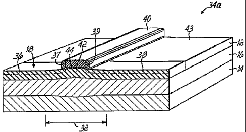
[033] With particular reference to FIG. 5, one type of semiconductor devices
34a may be
metal-oxide-semiconductor field effect transistors (MOSFET's) each having
source/
drain regions 36, 38 and an electrostatically-coupled gate electrode 40
located above a
channel 42 defined in the active layer 12 between the source/drain regions 36,
38. A
thin gate dielectric 44 insulates the gate electrode 42 electrically from the
channel 42.
The material used to form the gate electrode 42 may be, for example,
polysilicon,
tungsten, or any other desired material and the source/drain regions 36, 38
and their
extensions may be supplied by ion implantation of suitable dopant species.
Sidewall
spacers 37, 39 of a material such as silicon nitride may be added to the
vertical
sidewalls of the gate electrode 42 as is well known in the art. The spacers
37, 39 and
the gate electrode 42 collectively serve as a self-aligned mask for
implantation of the
deep doped portions of the source/drain regions 36, 38. Isolation regions 43
provide
electrical isolation between adjacent islands 18 of active layer 12. The
isolation regions
43 are filled with an appropriate dielectric material, such as silicon dioxide
deposited
conformally by chemical vapor deposition (CVD), that is polished flat and
planarized
CA 02559219 2006-09-08
WO 2005/096372 PCT/EP2005/051319
8
by a chemical-mechanical polishing (CMP) process or any other suitable
planarization
technique. The capping layer 22 acts as a polish stop for the planarization
operation
and is removed after the planarization operation.
[034] Carriers flow between the source/drain regions 36, 38 through the
channel 42 in
proportion to the variation in electrical resistivity in the channel 42, which
varies in
proportion to voltage applied to the gate electrode 40. The devices 34a are
fabricated
such that each channel 42 coincides with one of the strained regions 32. In
certain em-
bodiments of the invention, the devices 3a4 are n-channel field effect
transistors
(NFET's) and any p-channel field effect transistors (PFET's) present in the
integrated
circuit are formed in areas of the SOI substrate 10 lacking the strained
regions 32. The
field effect transistors are formed by a conventional fabrication process
familiar to
persons of ordinary skill in the art.
[035] With particular reference to FIGS. 6A and 6B, another type of
semiconductor
devices 34b may be self-aligned double gate fin field effect transistors
(finFET) each
having a thin vertical layer (fin) furnishing a channel 46 and a gate
electrode 48
defining two individual gate portions 48a, 48b (FIG. 5C) that flank the
channel region
46. The gate electrode 48 is positioned between source/drain regions 50, 52
and
overlies the channel 46. Gate electrode 48 is electrically isolated from gate
electrode
48 by a gate dielectric 47. Spacers 54, 56 are provided that flank the gate
electrode 48.
The device 34b is fabricated such that the channel 46 coincides with the
strained region
32. The invention contemplates that all or a portion of capping layer 22 may
remain on
the active layer 12 in the completed device structure. The finFET is formed by
a con-
ventional fabrication process familiar to persons of ordinary skill in the
art.
[036] With reference to FIG. 7 in which like reference numerals refer to like
features in
FIG. 2, a pad layer 58 may be applied to the capping layer 22 before the mask
24 is
applied and patterned. The pad layer 58 is any material that operates as an
etch stop
during the etch that patterns mask 24 and the etch that removes mask 24. The
pad layer
58 effectively prevents these individual etch processes from thinning the
capping layer
22 between stripes 26. One suitable material for pad layer 58 is silicon
dioxide, if the
capping layer 22 is silicon nitride, approximately 2 nanometers to
approximately 10
nanometers in thickness. Excessive thinning of capping layer 22 will reduce
its ef-
fectiveness as a polish stop and oxidation mask.
[037] While the present invention has been illustrated by a description of
various em-
bodiments and while these embodiments have been described in considerable
detail, it
is not the intention of the applicants to restrict or in any way limit the
scope of the
appended claims to such detail. Additional advantages and modifications will
readily
appear to those skilled in the art. Thus, the invention in its broader aspects
is therefore
not limited to the specific details, representative apparatus and method, and
illustrative
CA 02559219 2006-09-08
WO 2005/096372 PCT/EP2005/051319
9
example shown and described. Accordingly, departures may be made from such
details
without departing from the scope of applicants' general inventive concept.