Note: Descriptions are shown in the official language in which they were submitted.
CA 02563566 2006-10-18
WO 2005/107072 PCT/CA2005/000640
TENSIONED TOUCH PANEL AND METHOD OF MAKING SAME
Field of the Invention
[0001] The present invention relates generally to touch systems and in
particular to a tensioned touch panel and method of making the same
Background of the Invention
[0002] Touch panels such as for example digitizers and analog resistive touch
screens that make use of one or more tensioned membranes, are known in the
art.
Tensioned touch panels of this nature typically include a conductive membrane
that is
stretched tautly over and spaced from a conductive substrate. When a pointer
is used
to contact the tensioned membrane with sufficient activation force, the
tensioned
membrane deflects and contacts the conductive substrate thereby to make an
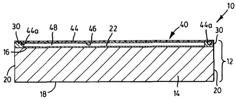
electrical
contact. Determining voltage changes induced by the electrical contact allows
the
position of pointer contact on the tensioned touch panel to be determined.
[0003] In order for such tensioned touch panels to work effectively, the
spacing between the tensioned membrane and the conductive substrate must be
maintained so that the tensioned membrane only contacts the conductive
substrate
when a pointer contact is made on the tensioned membrane.
[0004] As will be appreciated, over time the tensioned membrane may sag
creating slack in the tensioned membrane. Changes in environmental conditions
such
as humidity and/or temperature may also cause the tensioned membrane to expand
resulting in slack developing in the tensioned membrane. If the tensioned
membrane
sags or expands, the slack developed in the tensioned membrane may result in
undesirable contact between the tensioned membrane and the conductive
substrate.
This problem becomes more severe as the size of the touch panel becomes
greater.
[0005] A number of techniques have been considered to avoid undesirable
contact between the tensioned membrane and the conductive substrate. For
example,
electrically insulating spacer dots may be disposed between the tensioned
membrane
and the conductive substrate at spaced locations over the active contact area
of the
touch panel to maintain the spacing between the tensioned membrane and the
conductive substrate. U.S. Patent No. 5,220,136 to Kent discloses a contact
touchscreen including such insulating spacer dots.
[0006] Although the use of insulating spacer dots maintains separation
CA 02563566 2006-10-18
WO 2005/107072 PCT/CA2005/000640
_2_
between the tensioned membrane and the conductive substrate, the use of
insulating
spacer dots is problematic. In order to maintain separation between the
tensioned
membrane and the conductive substrate over the active contact area of the
touch
panel, the insulating spacer dots must be positioned at locations within the
active
contact area. Thus, the insulating spacer dots interrupt the active contact
area of the
touch panel. As a result, contacts with the tensioned membrane over insulating
spacer
dots will not register as contacts since the tensioned membrane cannot be
brought into
electrical contact with the conductive substrate at those contact points.
Also, the use
of insulating spacer dots to sepaxate the tensioned membrane and the
conductive
substrate is expensive. It is also difficult to maintain an even spacing
between the
tensioned membrane and the conductive substrate over the active contact area
using
insulating spacer dots.
[0007] U.S. Patent No. 5,838,309 to Robsky et al. discloses a self tensioning
membrane touch screen that avoids the need for insulating spacer dots. The
touch
screen includes a support structure having a base and a substrate support on
which a
conductive surface is disposed. A peripheral insulating rail surrounds the
conductive
surface. A peripheral flexible wall extends upwardly from the base. A
conductive
membrane is stretched over the conductive surface and is attached to the
peripheral
flexible wall. The insulating rail acts to space the conductive membrane from
the
conductive surface. To inhibit sagging and maintain tension on the conductive
membrane, during assembly of the touch screen the conductive membrane is
attached
to the flexible wall when the flexible wall is in a pretensioned state. In the
assembled
condition, the flexible wall is biased outwardly and downwardly. As a result,
tension
is continuously applied to the conductive membrane by the flexible wall
thereby to
inhibit sagging of the conductive membrane.
[0008] U.S. Patent No. 6,664,950 to Blanchard discloses a resistive touch
panel having a removable, tensioned top layer and a base plate. The touch
panel may
be situated relative to a display screen such that an air gap exists between
the base
plate and the display screen. The top plate includes a transparent, flexible
substrate
having a hard transparent coating, one or more anti-reflective coatings and an
anti-
fingerprint coating thereon. The underside of the substrate is spaced from the
upper
surface of the base plate by an air gap. To prevent wrinkling of the top
plate, a stiff
CA 02563566 2006-10-18
WO 2005/107072 PCT/CA2005/000640
-3-
frame is bonded to the anti-fingerprint coating. The stiff frame maintains
tension in
the top plate despite temperature changes.
[0009] Although the above references show touch panels having mechanisms
to maintain tension in the conductive membrane, manufacturing and labour costs
are
associated with these tensioning mechanisms. Accordingly, improvements in
tensioned touch panels to maintain the spacing between the tensioned membrane
and
the conductive substrate are desired.
[0010] It is therefore an object of the present invention to provide a novel
tensioned touch panel and method of making the same.
Summary of the Invention
[0011] According to one aspect of the present invention there is provided a
method of assembling a touch panel including a support structure and a
conductive
membrane.. The support structure has a conductive surface and a peripheral
insulating
spacer about the conductive surface. The conductive membrane overlies the
support
structure with the spacer separating the conductive membrane and the
conductive
surface thereby to define an air gap therebetween. During the method, the
conductive
membrane is pretensioned and the tensioned conductive membrane is secured to
the
support structure.
[0012] The pretensioning in one embodiment is selected to compensate for
both the coefficients of thermal expansion and hydroscopic or hygroscopic
expansion
of the conductive membrane over a variety of temperature and humidity
conditions.
The stress level is selected to be below the yield point of the conductive
membrane
and at a level below which the conductive membrane exhibits significant creep
i.e.
creep where the tension in the conductive membrane drops over time to a level
resulting in an unacceptable decrease in activation force and/or unwanted
contact
between the conductive membrane and the conductive surface. The conductive
membrane is bonded to the support structure via an adhesive such as for
example an
ultraviolet curing or cyanoacrylate (CA) adhesive.
[0013] The support structure includes a generally planar surface on which the
conductive surface is disposed. The spacer is generally continuous and
overlies the
peripheral region of the planar surface thereby to surround the conductive
surface.
CA 02563566 2006-10-18
WO 2005/107072 PCT/CA2005/000640
-4-
The conductive membrane may be adhered directly to the spacer or pulled around
the
spacer and adhered to the support structure.
[0014] According to another aspect of the present invention there is provided
a tensioned touch panel comprising a support structure including a substrate
having a
generally planar conductive surface disposed thereon and an insulating spacer
generally about the periphery of the substrate. A pretensioned conductive
membrane
overlies the support structure. The spacer separates the conductive membrane
and the
conductive surface thereby to define an air gap therebetween. The conductive
membrane is secured to the support structure under sufficient tension to
inhibit slack
from developing in the conductive membrane as a result of changes in
environmental
conditions.
[0015] According to yet another aspect of the present invention there is
provided a tensioned touch panel comprising a support structure having a
conductive
surface disposed thereon. A conductive membrane overlies the conductive
surface in
spaced apart relation. The conductive membrane is permanently secured to the
substrate while under tension.
[0016] The present invention provides advantages in that an overall uniform
tension can be maintained in the conductive membrane while reducing
manufacturing
and labour costs of the tensioned touch panel. As a result, slack is inhibited
from
developing in the conductive membrane regardless of environmental conditions
while
maintaining activation forces at user acceptable levels.
Brief Description of the Drawings
[0017] ~ Embodiments of the present invention will now be described more
fully with reference to the accompanying drawings in which:
Figure 1 is a side cross-sectional view of a tensioned touch panel;
Figure 2 is an enlarged portion of Figure 1;
Figure 3 shows steps performed during assembly of the tensioned
touch panel of Figure 1;
Figure 4 is a graph showing the stress versus strain characteristics of a
sample length of a conductive membrane and the theoretical stress versus
strain
characteristics of the conductive membrane film;
CA 02563566 2006-10-18
WO 2005/107072 PCT/CA2005/000640
-5-
Figure 5 is a graph showing the theoretical strain versus activation
force characteristics of the conductive membrane;
Figure 6 is a graph showing the creep characteristics of the conductive
membrane;
Figure 7 is a graph showing cyclical elongation versus time
characteristics of the conductive membrane filin when subjected to alternating
tensions of 8500 psi and zero psi respectively;
Figure 8 is a front plan view of the tensioned touch panel of Figure 1 in
an interactive display system;
Figure 9 is a side cross-sectional view of another embodiment of a
tensioned touch panel;
Figure 10 is a side cross-sectional view of yet another embodiment of a
tensioned touch panel;
Figure 11 is a side cross-sectional view of yet another embodiment of a
tensioned touch panel;
Figure 12 is a side cross-sectional view of still yet another embodiment
of a tensioned touch panel; and
Figure 13 is a side cross-sectional view of still yet another embodiment
of a tensioned touch panel.
Detailed Description of the Preferred Embodiments
[0018] Turning now to Figures 1 and 2, a tensioned touch panel is shown and
is generally identified by reference numeral 10. Touch panel 10 in this
embodiment is
generally rectangular and includes a support structure 12. Support structure
12
comprises a substrate 14 having a major top surface 16, a major bottom surface
18
and sides 20 bridging the top and bottom surfaces. The substrate 14 is formed
of a
rigid stable material such as for example aluminum or other suitable rigid
material. A
conductive carbon resistive layer 22 is bonded to the top surface 16 of the
substrate 14
via an adhesive. A peripheral insulating spacer rail 30 is disposed on the top
surface
16 of the substrate 14. The insulating spacer rail 30 is formed of
electrically
insulating material such as for example rigid polyvinyl chloride (RPVC),
acrylonitrile
CA 02563566 2006-10-18
WO 2005/107072 PCT/CA2005/000640
-6-
butadiene styrene (ABS), acrylic, fiberglass reinforced plastic (FRP) or
coated
aluminum and is bonded to the substrate 14 via an adhesive.
[0019] A flexible, elastic conductive membrane 40 under tension overlies the
support structure 12 and is secured to the insulating spacer rail 30 by a fast
drying
adhesive such as for example, ultraviolet curing or cyanoacrylate (CA)
adhesive. The
conductive membrane 40 is layered and includes an upper flexible, low creep
film 44
such as for example polyethylene terephthalate (PET) and a lower conductive
carbon
resistive layer 46 bonded to the film 44 by adhesive. The conductive resistive
layer
46 overlies the film 44 in the region corresponding to the active area of the
tensioned
touch panel 10. Thus, a peripheral region 44a of the film is free of the
conductive
resistive layer 46 allowing the film 44 to be adhered directly to the
insulating spacer
rail 30.
[0020] The tension applied to the conductive membrane 40 maintains
separation between the conductive membrane 40 and the conductive resistive
layer 22
on the top surface 16 of the substrate to define an air gap 48. In particular,
the tension
.applied to the conductive membrane 40 before being bonded to the insulating
spacer
rail 30 is selected to ensure that the air gap 48 is maintained over a
significant length
of time and over a variety of environmental conditions without signficantly
increasing the activation force required to bring the conductive resistive
layers 22 and
46 into electrical contact in response to a contact made on the tensioned
touch panel
10. In this manner, slack does not develop in the conductive membrane 40
making
the tensioned touch panel 10 robust.
[0021] The tensioned touch panel 10 operates in a manner similar to
conventional touch panels. When a pointer is used to contact the tensioned
conductive membrane 40 with sufficient activation force, the conductive
resistive
layer 46 is brought into contact with the conductive resistive layer 22 at the
contact
location. Voltage changes induced by the electrical contact between the
conductive
resistive layers 22 and 46 are sensed allowing the position of the pointer
contact to be
determined.
[0022] Turning to Figure 3, the steps performed during assembly of the
tensioned touch panel 10 are illustrated. The conductive membrane 40 is
initially
placed in an assembly fixture and is stretched in both its lengthwise and
widthwise
CA 02563566 2006-10-18
WO 2005/107072 PCT/CA2005/000640
directions to place the conductive membrane 40 under tension. During
stretching of
the conductive membrane 40, the conductive membrane 40 is subj ected to stress
generally in the range of from about 1000 to 1500 pounds per square inch
(psi). It has
been found that this pretensioning of the conductive membrane 40 is sufficient
to
ensure effective operation of the tensioned touch panel 10 over a variety of
environmental conditions while maintaining the activation force required to
bring the
conductive resistive layers 22 and 46 into electrical contact at user
acceptable levels.
With the conductive membrane 40 under the desired amount of tension, adhesive
is
placed on the peripheral region 44a of the film 44 that is free of the
conductive
resistive layer 46 in a pattern corresponding to the insulating spacer rail
30.
Alternatively the adhesive may be placed on the insulating spacer rail 30 or
on both
the peripheral region 44a of the film 44 and the insulating spacer rail 30.
The support
structure 12 is then brought into contact with the tensioned conductive member
40 to
enable a secure bond to be formed between the insulating spacer rail 30 and
the
tensioned conductive membrane 40. Once the adhesive cures, the conductive
membrane 40 is released from the assembly fixture. Excess length of conductive
membrane 40 extending beyond the insulating spacer rail 30 is removed.
[0023] As mentioned above, the tension applied to the conductive membrane
40 is selected to inhibit slack from developing in the conductive membrane by
using
the conductive membrane 40 itself as the means of maintaining tension. The end
result is a highly reliable, robust touch panel 10 that can be easily
manufactured in a
low cost manner. In particular, the tension applied to the conductive membrane
40
prior to attachment to the insulating spacer rail 30 is selected to compensate
for the
coefficient of thermal expansion (CTE) and the coefficient of hydroscopic or
hygroscopic expansion (CHE) of the conductive membrane 40 without exceeding
the
yield point of the conductive membrane 40 and while maintaining the activation
force
at user acceptable levels. By tensioning the conductive membrane 40 in this
manner,
the conductive membrane 40 remains wrinkle free throughout a wide range of
temperature and humidity conditions while ensuring that an adequate, but not
excessive, activation force is required to bring the conductive resistive
layers 22 and
46 into contact in response to a contact made on the tensioned touch panel 10.
The
CA 02563566 2006-10-18
WO 2005/107072 PCT/CA2005/000640
_g_
tension of the conductive membrane 40 simply reduces or increases depending on
the
temperature and humidity conditions while remaining wrinkle free.
[0024] A number of tests were performed on the conductive membrane 40 to
ensure its suitability. During testing, the effect of the conductive resistive
layer 46 on
the film 44 was assumed to be negligible to the overall characteristics of the
conductive membrane 40 since the conductive resistive layer 46 and bonding
adhesive
are both very thin and pliable as compared to the film 44. It was also assumed
that
the conductive membrane 40 behaves in a linear fashion with respect to CTE and
CHE and that the activation force is a linear function of tension applied to
the
conductive membrane 40. Creep of the conductive membrane 40 was not considered
to be a critical factor at the level of tension applied to the conducive
membrane 40
during assembly of the touch panel 10. The conductive membrane 40 was also
assumed to behave the same in both the lengthwise and widthwise directions.
[0025] Table 1 below shows the amount of elongation of a sample length of
the conductive membrane 40 for various stresses applied to the conductive
membrane
sample.
Cross 0.14125 Inches~2
sectional
area
of sam
le
Sample 41.375 Inches
length
Force Sample elongation (inches)stress % elongation
si
lbs
0.0 0 0 0.00000
11.8 0.004 84 0.00967
16.0 0.008 113 0.01934
22.0 0.011 156 0.02659
32.4 0.016 229 0.03867
50.4 0.021 357 0.05076
73.0 0.033 517 0.07976
86.0 0.036 609 0.08701
100.8 0.045 714 0.10876
119.4 0.052 845 0.12568
136.0 0.06 963 0.14502
155.8 0.067 1103 0.16193
169.5 0.072 1200 0.17402
178.6 0.076 1264 0.18369
187.0 0.078 1324 0.18852
189.0 0.079 1338 0.19094
CA 02563566 2006-10-18
WO 2005/107072 PCT/CA2005/000640
-9-
199.0 0.086 1409 0.20785
Table 1
Figure 4 is a graph showing the stress versus strain data of Table 1 together
with the
theoretical stress versus strain characteristics of the film 44. As will be
appreciated,
the behaviour of the conductive membrane 40 corresponds very well with the
theoretical stress .versus strain data.
[0026] The relative change in dimension between the conductive membrane
40 and the support structure 12 at a variety of environmental conditions were
calculated for a tensioned touch panel 10 having an active contact area 60
inches in
length and 48 inches in width. For the purpose of these calculation, the
following
assumptions were made:
Conductive membrane CTE: 0.000017 in/in/°C
Conductive membrane CHE: 0.00006 in/in/%RH
Support structure CTE: 0.0000237 in/in/°C
Temperature during assembly: 21°C
Humidity during assembly: 44%
[0027] Based on the above assumptions and looking at the longest dimension
of the conductive membrane 40 where changes are greater than in the shorter
dimension, the change in the size of the conductive membrane 40 for each
1°C
increase in temperature above the assembly temperature can be calculated as
follows:
0.000017"/"/° * 60" * 1 ° = 0.00102"
[0028] The change in size of the support structure 12 for each 1°C
increase in
temperature above the assembly temperature can be calculated as follows:
0.0000237"/"/° * 60" * 1 ° = 0.00142"
[0029] The change in size of the conductive membrane 40 for each 1
increase in relative humidity (RH) above the assembly humidity can be
calculated as
follows:
0.000006"/"/% * 60" * 1% = 0.00036"
CA 02563566 2006-10-18
WO 2005/107072 PCT/CA2005/000640
-10-
[0030] The effects of the CTE and CHE are cumulative for the conductive
membrane 40, so for a 1 °C temperature increase and a 1 % increase in
relative
humidity, the net change in size of the conductive membrane 40 is:
0.00102" + 0.00036" = 0.00138"
[0031] The relative change in size between the conductive membrane 40 and
the support structure 12 for a 1 °C temperature increase and a 1 %
increase in relative
humidity above the assembly conditions is therefore:
0.0013 8" - 0.00142" _ -0.00004"
[0032] The negative number indicates that the conductive membrane 40 grew
less than the support structure 12. Since the conductive membrane 40 is
rigidly and
permanently bonded to the support structure 12, the conductive membrane 40 was
stretched by the support structure 12 an amount equal to 0.00004"
[0033] An interactive analysis of the effects of temperature and humidity was
performed using the above calculations to allow the changes in size of the
conductive
membrane to be calculated over a variety of enviromnental conditions differing
from
assembly conditions. For example, consider the following assembly and in
service
conditions where the in service conditions represent a typical office
environment:
Assembly conditions: 20°C @ 40% RH
In service conditions: 23°C @ 60% RH
In these in service conditions, the size of the conductive membrane 40 would
increase
by 0.006".
[0034] Consider more severe in service conditions that may represent a
shipping environment:
Assembly conditions: 20°C @ 35% RH
In service conditions: 50°C @ 95% RH
In these in service conditions, the size of the conductive membrane 40 would
increase
by 0.009".
[0035] Consider opposite end extreme in service conditions that may also
represent a shipping environment:
CA 02563566 2006-10-18
WO 2005/107072 PCT/CA2005/000640
-11-
Assembly conditions: 20°C @ 35% RH
In service conditions: -40°C @ 15% RH
In these in service conditions, the size of the conductive membrane would
increase by
0.016".
[0036] During assembly of the touch panel 10, the conductive membrane 40 is
stretched by more than the above calculated amounts prior to being attached to
the
insulating spacer rail 30 of the support structure 12. As a result, changes in
environmental conditions causing the conductive membrane 40 to expand do not
create slack in the conductive membrane 40. Rather these environmental changes
affect the tension, or stress in the conductive membrane 40 and therefore,
simply alter
the activation force. Since the activation force generated by a certain strain
is known,
the activation force can be plotted as a line as shown in Figure 5.
[0037] Line 60 in the graph of Figure 5 shows the theoretical relationship
between strain of the conductive membrane 40 and the resulting activation
force. The
intersection point of line 62 and line 60 represents the activation force
required to
bring the conductive resistive layers 22 and 46 into electrical contact at
assembly
conditions of 21°C @ 44% RH. The intersection point of line 64 and line
60
represents the activation force required to bring the conductive resistive
layers 22 an
46 into electrical contact at environmental conditions of 40°C @ 85%
RH. The
difference along the x-axis between the two intersection points represents the
resulting change in activation force. In the above example, there is a
decrease in
activation force equal to about 6 or 7 grams.
[0038] Creep of the conductive membrane 40 after assembly of the touch
panel 10 is also of concern. If the conductive membrane 40 were to creep
significantly after assembly of the touch panel 10, the activation force would
drop
gradually as the internal stress of the conductive membrane 40 relaxed. Creep
data
for the film 44 is shown in Figure 6. The graph depicts creep as the change in
elongation over time at a fixed stress. The flatter the line, the less creep
exhibited by
the film 44. As can be seen, creep is very low at the tension used to
pretension
conductive membrane 40 during assembly. The line is very flat at stresses in
the 1000
to 1500 psi range.
CA 02563566 2006-10-18
WO 2005/107072 PCT/CA2005/000640
-12-
[0039] The effect of cyclical, or alternating stresses is also of concern in
that
the touch panel 10 may encounter many changes in environmental conditions
during
shipping. Figure 7 shows data for the film 44 when the film is subj ected to
alternating
tensions of 8500 psi and zero psi respectively. As can be seen, the film 44
exhibits a
slight creep under these conditions as the bottom of each cycle is slightly
higher than
the previous cycle. Since the strain applied to the conductive membrane 40
during
assembly of the touch panel 10 and over a variety of environmental conditions
is
significantly less than 8500 psi, it is believed that the effect of cyclical,
or alternating
stresses will be negligile.
[0040] Figure 8 shows the tensioned touch panel 10 in an interactive touch
system 100 of the type disclosed in U.S. Patent No. 5,448,263 to Martin, the
content
of which is incorporated herein by reference. As can be seen, the tensioned
touch
panel 10 is coupled to a computer 102. Computer 102 provides image data to a
projector 104 which in turn projects an image 106 on the touch panel 10.
Sensed
pointer contacts on the touch panel 10 that are sufficient to bring the
conductive
resistive layers 22 and 46 into electrical contact are conveyed to the
computer 102,
which in turn updates the image data conveyed to the projector 104 so that the
image
106 projected on the touch panel 10 reflects pointer contacts. The touch panel
10,
computer 102 and projector 104 thus form a closed loop. Alternatively, the
tensioned
touch panel 10 may be used in conjunction with a rear proj ection system.
[0041] Figure 9 shows another embodiment of a tensioned touch panel 110
similar to that of Figure 1. In this embodiment, the conductive resistive
layer 146
adhered to the film 144 overlies the entire surface of the film 144 that faces
the
support structure 12 thereby eliminating the peripheral margin 44a.
[0042] Figure 10 shows yet another embodiment of a tensioned touch panel
210. In this embodiment, the insulating spacer rail 230 is generally L-shaped
in
section. One arm 230a of the insulating spacer rail 230 overlies the periphery
of the
top surface 216 of the substrate 214. The other arm 230b of the insulating
spacer rail
230 abuts the sides 220 of the substrate 214.
[0043] Figure 11 shows yet another embodiment of a tensioned touch panel
310. In this embodiment the insulating spacer rail 330 is C-shaped in section
and
completely surrounds the sides 320 of the substrate 314. The upper arm 330a of
the
CA 02563566 2006-10-18
WO 2005/107072 PCT/CA2005/000640
-13-
insulating spacer rail 330 overlies the periphery of the top surface 316 of
the substrate
314. The lower arm 330b of the insulating spacer rail 330 overlies the
periphery of
the bottom surface 318 of the substrate 314. The bight 330c of the insulating
spacer
rail 330 abuts the sides 320 of the substrate 314. The conductive membrane 340
is
similar to that shown in Figure 1 and is bonded to the top surface of the
upper arm
330a.
[0044] Figures 12 and 13 show still yet further embodiments of tensioned
touch panels 410 and 510 respectively similar to that of Figure 11. In Figure
12, the
conductive membrane 440 overlies the entire outer surface of the insulating
spacer rail
430 and is bonded to the upper and lower arms 430a and 430b as well as the
bight
430c of the insulating spacer rail 430. In the embodiment of Figure 13, the
conductive membrane 540 also overlies the entire outer. surface of the
insulating
spacer rail 530 but extends beyond the lower arm 530b of the insulating spacer
rail
530 and is bonded to the bottom surface 518 of the substrate 514.
[0045] Although the conductive membranes illustrated in Figures 10 to 13
show the conductive resistive layer covering the entire surface of the film
that faces
the support structure, conductive membranes of the form shown in Figure 1 can
of
course be used.
[0046] Although a number of embodiments of the tensioned touch panel have
been described and illustrated, those of skill in the art will appreciate that
other
variations and modifications may be made without departing from the spirit and
scope
thereof as defined by the appended claims. For example, the support structure
need
not be rectangular. The present method allows tensioned touch panels of
virtually any
shape to be constructed. Ultraviolet and CA adhesives were selected to secure
the
conductive membrane to the support structure due to their fast cure times.
Other
suitable adhesives can of course also be used. The peripheral insulating
spacer rails
need not to be adhered to the support structure. Other suitable fastening
means may
of course be used to secure the insulating spacer rails to the support
structure.