Note: Descriptions are shown in the official language in which they were submitted.
CA 02565454 2006-11-02
WO 2005/105276 PCT/NL2005/000331
1
Device with a membrane on a'carrier, as well as a method for manufacturing
such a membrane
The invention relates to a device, in particular for filtration of liquids,
comprising a
membrane on a carrier. The invention also relates to a method for
manufacturing a
device with a membrane on a carrier. The invention further relates to
application of a
device with a membrane on a carrier according to the invention as well as to a
module
comprising such a membrane on a carrier. The invention also relates to a
method for
determining fracture in such a membrane on a carrier.
A filtration membrane is known from American patent US 5,753,014. This
filtration
membrane comprises a membrane with membrane openings. These membrane
openings have a pore size of 5 nm (nanometres) to 50 micrometres. The membrane
can be formed by deposition of a thin layer on a carrier by means of for
instance a
suitable vapour deposition or spin coating. Perforations are then made in the
thus
formed membrane, for instance by means of etching after a lithography step. It
is
further stated that such a membrane can serve as a carrier for the deposition
of a
separating layer, for instance for ultrafiltration, gas separation or
catalysis.
If a carrier is present, this carrier can be etched away completely or be
provided with
carrier openings having a diameter greater than that of the membrane openings
in the
membrane. In the first case only the membrane remains, in the second case the
membrane is supported by the carrier.
A drawback of such membrane filters according to this American patent is
however
that they are mechanically weak. The walls of the carrier openings of the thus
formed
membrane carriers consist substantially of crystal surfaces if crystalline
starting
material is used, for instance the <111> orientation in the case of [100] or
[110]
silicon. This mechanism is inherent to the method applied in this American
patent.
This means that in the case of mechanical load possibly present fracture lines
can
easily lead to fracture of the carrier, and thus of the filtration membrane.
CA 02565454 2006-11-02
WO 2005/105276 PCT/NL2005/000331
2
Although it is further possible with the techniques known at the time of this
American
patent to etch a pattern in the outer part of a carrier or in a layer applied
thereto,
etching of this pattern through the carrier entails significant drawbacks.
With these
techniques it is for instance not possible, or hardly so, to prevent
underetching (see
figure 2). In this respect underetching is understood to mean the phenomenon
known
to the skilled person wherein etching takes place under a protective layer
such as a
lacquer coat. The underlying structure is hereby unintentionally affected
adversely.
Furthermore, in the case a silicon [100] or [110] wafer is used and an
anisotropic
etching technique is used, round or almost round carrier openings are not
obtained.
The <111> directions after all determine the preferred etching directions in
this case,
whereby diamond-shaped carrier openings are formed, which are also tapering.
Each
carrier opening which does not run substantially straight further has the
further
drawback that the flow through such a carrier opening is further obstructed.
Nor is it
possible with the filtration membranes formed in this US 5,753,014 patent to
monitor
the integrity of the membrane and/or carrier without interrupting the
production in a
device. This is disadvantageous for the degree of capacity utilization of such
a device.
With such a membrane according to the US 5,753,014 patent it is further not
possible
to monitor the action in respect of for instance filtration efficiency and
microscopic
fractures.
An object of the present invention it to provide a strengthened membrane on a
carrier.
In order to achieve the intended object, a membrane on a carrier of the type
stated in
the preamble has the feature according to the invention that the carrier
opening has a
rounded cross-section.
Surprisingly, it has been found that if the carrier openings have a rounded
cross-
section an improved mechanical strength is obtained. If the rounding has a
radius of
curvature greater than 3 micrometres and preferably greater than 5
micrometres, the
CA 02565454 2006-11-02
WO 2005/105276 PCT/NL2005/000331
3
mechanical strength of the membrane can then increase by more than 50%
compared
to carrier openings in which there are local imperfections or edges with a
smaller
radius of curvature. This strength can surprisingly be increased further by
embodying
the carrier openings with a very low surface roughness of smaller than 3
micrometres,
and in particular smaller than 0.3 micrometres, whereby crack initiation is in
large
measure prevented.
If the surface roughness is smaller than 3 micrometres, the mechanical
strength is then
improved by a minimum of about 30%. At a surface roughness lower than 0.3
micrometres, it is improved by a minimum of 80%. The mechanical strength is
determined by clamping and then loading the membrane with carrier relatively
uniformly and herein determining the failure pressure.
For filtration applications the membranes with carrier are usually clamped and
supported in a membrane holder which is provided with a number of parallel
support
bars. The distribution and the size of the carrier openings in the carrier of
the
membrane relative to said support bar can, if desired, be optimized so that
the stress
distribution of the carrier is distributed as optimally as possible.
A particular embodiment with a high mechanical load-bearing capacity has the
feature
that a pattern of carrier openings is arranged in the carrier such that a
first part-pattern
has a high density of carrier openings, a second part-pattern adjacent to the
first part-
pattern has a less high density of carrier openings, and a third part-pattern
adjacent to
the second part-pattern has a very low or no density of carrier openings in
order to
clamp the membrane with carrier in a membrane holder without damage, and
wherein
mechanical stress build-up in the carrier is also reduced. Density is here
understood to
mean a measure for the open surface area of openings in relation to a given
total
surface area. The density in the second part-pattern is preferably less than
half the
density in the first part-pattern. The mechanical strength can thus be
improved by a
minimum of 30%. In another embodiment the density of carrier openings is not
modified in stepwise manner per part-area but this density varies smoothly in
order to
CA 02565454 2006-11-02
WO 2005/105276 PCT/NL2005/000331
4
distribute the mechanical stress build-up as well as possible, the mechanical
strength
hereby being improved by a minimum of 50%.
It has been found surprisingly that a significantly greater mechanical
strength (>20%)
is already obtained by providing the carrier with continuous elongate sieve
tracks. A
further embodiment of a device of the type stated in the preamble therefore
has the
feature according to the present invention that the carrier is provided with
continuous
sieve tracks. Continuous is here understood to mean that the sieve tracks are
not
interrupted by for instance strips placed perpendicularly thereof, in which no
carrier
openings are present. Extra strength for the membrane on the carrier is
obtained by
providing the carrier with such sieve patterns, without too much surface area
remaining unused for the actual filtering application.
A subsequent object of the present invention is to provide a membrane on a
carrier
which is provided with means enabling monitoring of the integrity of the
membrane
on a carrier.
Surprisingly, it has now been found that such a membrane on a carrier can be
obtained
by providing it with at least an electrical conductor. It is hereby even
possible to
monitor the integrity of the membrane on a carrier in the production process
itself.
The present invention therefore relates to a membrane on a carrier which is
provided
with at least one electrical conductor, with which the integrity of the
membrane as
well as the action of the membrane can be monitored without disrupting a
production
process.
A better degree of capacity utilization of production equipment and a better
controlled
action of the membrane are for instance hereby obtained.
A subsequent object of the present invention is to provide a method for
manufacturing
a strengthened membrane on a carrier.
CA 02565454 2006-11-02
WO 2005/105276 PCT/NL2005/000331
It has now been found, surprisingly, that by first etching a pattern in a
second side of a
carrier or in the layer applied thereto, and etching this through in a
subsequent step,
carrier openings are obtained which have a desired size, depth and tapering
without
the above mentioned drawbacks. The present invention therefore relates to a
method
5 for manufacturing such a membrane on a carrier.
A membrane on a carrier according to the invention is particularly suitable
for the
filtration of a fluid, in particular of liquids, since it has on the one hand
an excellent
and selectively separating capacity for particles of different sizes and can
on the other
hand be applied easily. A membrane on a carrier according to the invention is
otherwise also particularly suitable for the separation of particles with
different sizes
in a gas. This separation can even be improved further using two membranes in
series.
Particles with a specific size range can also be separated with two membranes
in
series by means of fractionation.
A membrane on a carrier according to the invention is moreover much better
able to
withstand the occurrence of fractures. This is a significant advantage because
for
instance the membrane on a carrier hereby needs much less frequent
replacement.
This improves the degree of capacity utilization of a process device. A
significant
advantage of fewer fractures is moreover that a separation continues to
proceed much
more homogeneously. In addition, much less fouling occurs compared to usual
filters.
The inventors believe this is caused by the thin and smooth surface of the
membrane.
Owing to a particular design of inter alia the membrane openings in the
membrane on
a carrier, the membrane on a carrier according to the invention can also be
back-
flushed and/or back-pulsed more easily compared to other filters, whereby
cleaning is
simplified and improved. This back-flushing and/or back-pulsing further
enhances
general filtration because the filtration proceeds better after flushing and
back-flushing
and/or back-pulsing are necessary less often or for less time, so that for
instance less
process time is lost.
CA 02565454 2006-11-02
WO 2005/105276 PCT/NL2005/000331
6
The membrane on a carrier according to the invention is furthermore much
stronger
than heretofore usual and comparable membranes, in the sense that it is
possible to
withstand much greater pressures.
Figure 1 shows a schematic cross-section of an example of a membrane on a
carrier.
Figure 1 describes a membrane 13 provided with membrane openings 14 and a
carrier
11 which is covered on two sides with an extra layer 12, wherein layer 13 can
be an
optionally protective layer. Layer 13 is for instance a layer of Si3N4, layer
12 is for
instance a layer of SiO2, layer 11 is in that case crystalline Si, and 15 is a
carrier
opening in the carrier. Layer 12 is otherwise not strictly necessary and can
be omitted
in appropriate cases.
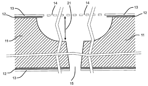
Figure 2 shows a schematic cross-section of a comparable membrane on a
carrier. The
carrier is now provided with an additional "cup" 21. This cup is obtained by
two
etching steps instead of one. The underside is etched with an etching
technique
(DRIE) other than the upper side (isotropic wet chemical through the membrane)
(see
below for detail). An advantage is that a relatively large amount of Si-
carrier material
remains, which results in a stronger wafer, while as much effective filtration
surface
area as possible is realized. Cup 21 has a cross-section which can be about
one to fifty
times the cross-section of carrier opening 15, and preferably two to ten
times. The
diameter of carrier opening 15 can also be chosen so small that it can
strongly limit
the liquid flow in the case the membrane has defects, wherein non-filtered
liquid can
come into direct contact with the filtered liquid. The flow resistance of
carrier opening
15 is preferably ten to fifty times lower than the flow resistance of membrane
field 14.
Figure 3 shows a schematic top view of an example of a membrane on a carrier,
such
as that of figure 2. The carrier is provided with carrier openings 31. The
rectangular
membrane fields 30 are arranged mutually offset and have a dimension of for
instance
250 by 2500 micrometres. The round openings 31 in the carrier have a diameter
of
200 micrometre, while the mutual distance 32 between openings 31 is a minimum
of
800 micrometres, which greatly enhances the mechanical strength of the carrier
while
CA 02565454 2006-11-02
WO 2005/105276 PCT/NL2005/000331
7
a large effective filtration surface area is obtained. The surface area of the
membrane
field is preferably two to twenty times greater than the cross-sectional area
of the
opening in the carrier.
Figure 4 shows a schematic bottom view of an example of a membrane on a
carrier,
such as that of figure 1. The carrier is provided with carrier openings 15.
For a high
mechanical load-bearing capacity the density of carrier openings is varied by
selecting
different sizes 41 for carrier openings 15 per part-pattern 42, 43, 44, while
the centre-
to-centre distance 45 of the carrier openings does not change, or hardly so.
The stress
distribution of the carrier can hereby be optimized. Close to support bar 46
the density
of the carrier openings is low, while towards the centre, between two support
bars, the
density of the carrier openings becomes higher.
A particular embodiment of a membrane on a carrier with a high mechanical load-
bearing capacity has the feature that a pattern of carrier openings is
arranged in the
carrier such that a first part-pattern 42 has a high density of carrier
openings, a second
part-pattern 43 adjacent to the first part-pattern has a less high density of
carrier
openings, and a third part-pattern 44 adjacent to the second part-pattern has
a very low
or no density of carrier openings, in order to clamp the membrane with carrier
in a
membrane holder without damage and wherein mechanical stress build-up in the
carrier is also reduced.
Figure 5 shows a variant of the example sketched in figure 4. In order to
optimize the
stress distribution in the carrier, in this figure it is not the size 41 of
the carrier
openings which is varied, but the centre-to-centre distance 45 between the
carrier
openings. This has the advantage that the etching process used, which is
optimized for
the diameter (a larger hole etches more rapidly), proceeds uniformly over the
carrier.
In a first embodiment, the invention relates to a membrane on a carrier
wherein the
carrier is provided with continuous sieve patterns.
CA 02565454 2006-11-02
WO 2005/105276 PCT/NL2005/000331
~
The term "membrane" is understood to mean a layer which is provided with
membrane openings. These membrane openings are highly uniform in respect of
size,
depth and shape. A membrane can consist of a material optionally deposited on
a
carrier. Suitable materials for the membrane are for instance inorganic or
ceramic
components such as silicon, carbon, silicon oxide, silicon nitride, silicon
oxynitride,
silicides, alumina, zirconium oxide, magnesium oxide, chromium oxide, titanium
oxide, titanium oxynitride, titaniuin nitride and yttrium-barium-copper
oxides. A
metal or an alloy with palladium, lead, gold, silver, chromium, nickel, steel,
a ferro-
alloy, tantalum, aluminium and titanium can also be used as membrane material.
The
membrane can preferably be of silicon carbide or a diamond-like carbon (DLC or
SP3)
layer, whereby higher mechanical loads are possible than for instance a
membrane
layer of silicon nitride is applied.
Another embodiment has the feature that the membrane is provided with a
chemically
inert, preferably hydrophilic coating layer, for instance a hydrophilic
plastic layer, or
an inorganic layer such as titanium oxide, carbide or silicon carbide. The
membrane
and/or a coating layer is further preferably electrically conductive, whereby
it is
possible during filtration and/or the cleaning to prevent fouling respectively
to remove
fouling. The thickness of this layer is preferably between 1 and 350
nanometres,
sufficient for prolonged chemical load and not unnecessarily thick, whereby
the
membrane openings become too small.
The carrier and the membrane can be composed of different materials and can,
if
desired, also be provided with an intermediate layer such as for instance
silicon oxide
to improve the mechanical properties of the membrane layer, or to protect the
membrane layer from for instance a reactive ion plasma during etching of the
carrier
openings in the carrier. Instead of silicon oxide a very thin titanium oxide
or
chromium oxide or other suitable oxide or nitride layer can for instance also
be
applied as etch stop layer.
CA 02565454 2006-11-02
WO 2005/105276 PCT/NL2005/000331
9
There are in fact not many limitations to the choice of a material of a
membrane. The
most important limitations are that a membrane must be compatible with a
carrier.
This means that a membrane and a carrier must be sufficiently connected to
each other
by chemical or physical bonding. This can optionally be achieved by means of
an
intermediate layer. A membrane must further be suitable for a chosen
application, it
must for instance be non-toxic and chemically inert. A preferred material for
a
membrane is however silicon nitride because of a relatively simple manner of
depositing and chemical inertness.
The term "carrier" designates a structure which is intended to support a
membrane.
Particularly the mechanical properties of a membrane are hereby improved,
without
other properties being too adversely affected.
The carrier is normally connected to the membrane, for instance by depositing
the
membrane on the carrier. Suitable materials for the carrier of the membrane on
a
carrier according to the invention are preferably composed of inorganic or
ceramic
components. Examples hereof are silicon, carbon, silicon oxide, silicon
nitride, silicon
oxynitride, silicon carbide, silicides, alumina, zirconium oxide, magnesium
oxide,
chromium oxide, titanium oxide, titanium oxynitride and titanium nitride and
yttrium-
barium-copper oxides. A metal or an alloy with palladium, tungsten, gold,
silver,
chromium, nickel, steel, a ferro-alloy, tantalum, aluminium and titanium can
also be
applied as a carrier material. A polyiner material can optionally be applied
for the
carrier, such as polyurethane, polytetrafluoroethylene (TEFLON), polyamide,
polyimide, polyvinyl, polymethyl methacrylate, polypropylene, polyolefin,
polycarbonate, polyester, cellulose, polyformaldehyde and polysulphone
For biomedical applications the carrier can be composed of a biocompatible
material
such as silicon nitride, silicon carbide, silicon oxynitride, titanium,
titanium oxide,
titanium oxynitride, titanium nitride, polyamide and polytetrafluoroethylene
(TEFLON). The carrier can also be provided with a biocompatible covering of
these
CA 02565454 2006-11-02
WO 2005/105276 PCT/NL2005/000331
materials, or be provided with another biocompatible covering, for instance a
heparin
covering.
The carrier can consist of a macroporous material such as a tortuous pore
structure, a
5 sintered ceramic material, a sintered metal powder or a tortuous polymer
membrane,
as well as of an initially closed material in which carrier openings are made
at a later
stage, for instance a semiconductor wafer, a metal carrier or an inorganic
disc. It is
further even possible to work with polycrystalline silicon, as is usual in the
solar cell
industry, which is economically advantageous, while no preferred crystal
orientations
10 are present so that a membrane on a carrier can be realized which can be
loaded a
minimum of 20% more.
The mask on a membrane side preferably comprises a pattern with rectangular
slots
having a dimension of 0.1 x 0.1 micrometres to 5.0 x 5.0 micrometres. The
advantage
of such slots is that they can be readily transferred with existing
lithographic
techniques and have a good action. These slots are sufficiently selective,
among other
reasons because they can be formed sufficiently homogeneously.
The precise dimensions of the slots are determined by the application.
Examples
hereof are the filtering of micro-organisms from milk: 0.6-0.9 by 2.0-4.0
micrometres,
filtering of fat 0.5-3.0 x 1.0-10 micrometres, filtering of proteins 0.05-0.1
x 0.1-0.5
micrometres.
The term "slot" is understood to mean a rectangular membrane opening. On the
carrier side the mask preferably further comprises a pattern with
substantially round
membrane openings with a diameter of 100 micrometres to 1000 micrometres, more
preferably with a diameter of 200 micrometres to 500 micrometres, most
preferably
with a diameter of 200 micrometres to 300 micrometres, wherein the sieve
pattern of
carrier openings lies in tracks 3-15 mm wide, with an unexposed space between
the
tracks of 1-8 mm. In a preferred embodiment these are tracks of about 8 mm
wide and
an intermediate space of about 3 mm. The thickness of the membrane is
preferably 50
CA 02565454 2006-11-02
WO 2005/105276 PCT/NL2005/000331
11
nm to 2 micrometres, very preferably 300 nm to 1.5 micrometre, most preferably
about 1 micrometre. The choice of the thickness of the membrane depends among
other factors on the choice of the size of the carrier openings in the
carrier. For
instance, if a thin membrane is chosen, the reduced strength hereof can be
compensated by arranging smaller carrier openings in the carrier. It will be
apparent to
the skilled person that, in combination with other features of the membrane on
a
carrier, such parameters can be easily modified to obtain the desired
properties such as
selectivity, strength. If the layer becomes too thick, the deposition moreover
takes
proportionately longer, which is economically unattractive. If the layer is
too thin, the
layer provides insufficient action, for instance because it then has an
insufficiently
homogeneous thickness over the relevant distance range, and the layer is then
not
strong enough. The membrane can be of the above mentioned materials and is
preferably of Si3N4.
Such a membrane on a carrier generally has sufficient strength to be able to
withstand
a pressure of about 7 bar, while membranes of similar type known heretofore
can
withstand only a pressure of a maximum of about 2 bar.
In a second embodiment, the invention relates to a membrane on a carrier
wherein the
carrier comprises carrier openings having walls with directions substantially
differing
from the preferred crystal orientation.
The term "crystal orientation" is here understood to mean a designation usual
in
crystallography for a vector related to the crystal lattice.
The term "preferred crystal orientation" refers to that orientation or those
orientations
occurring when a material such as a carrier is etched, particularly if the
material is
etched wet. In the case of Si for instance the <111> is the intended preferred
crystal
orientation in the case of a[100] surface. It is assumed that a drawback of
such a
preferred orientation is that the angles will be centres for stress during
load and will
CA 02565454 2006-11-02
WO 2005/105276 PCT/NL2005/000331
12
act as points for the initiation of fracture of the carrier, and therefore
also of the
membrane.
If the formed carrier openings in the carrier also lie in a disadvantageous
pattern (for
instance all square sides of a carrier opening lie at a<100> orientation), a
fracture
then occurs relatively quickly. A mechanism is hereby inherently present which
increases the chance of fracture along these dislocations, in particular in
the case of
mechanical load, which is disadvantageous for the lifespan of the membrane on
a
carrier.
In a typical example the carrier openings of the carrier will have a
substantially round
or oval cross-section, which to great extent prevents fracture formation.
In a third embodiment, the invention relates to a membrane on a carrier,
wherein the
walls of the carrier openings of the carrier are substantially perpendicular
to the
surface of the carrier, or have a positive tapering or a negative tapering, or
have a
combination hereof.
An example of such a meinbrane on a carrier is a carrier which is at least
partly
provided with carrier openings with a positively tapered profile. The angle of
the
profile relative to the normal of the carrier is in this case 1 to 25 degrees,
in particular
5 to 15 degrees, as shown schematically in figure 1. If the angle becomes too
great, the
flow through the membrane on a carrier will become too limited. On the other
hand,
more carrier material is present in the case of a greater angle, which
enhances the
strength.
By the term "tapering" is understood the angle between the normal
perpendicular to
the surface and a vector along a wall of the etched carrier opening in the
carrier. The
carrier opening has the form of a conical structure which can be practically
circular or
more or less elliptical.
CA 02565454 2006-11-02
WO 2005/105276 PCT/NL2005/000331
13
The term "positively tapered" is understood to mean a tapering wherein the
carrier
opening decreases in size from the outer surface of the carrier as seen in the
direction
of the membrane.
The term "negative tapering" designates a tapering wherein the carrier opening
increases in size from the outer surface of the carrier as seen in the
direction of the
membrane.
In a subsequent embodiment, the invention relates to a membrane on a carrier,
wherein the membrane and the carrier are each provided with a chemically inert
protective layer. This layer is preferably a hydrophilic protective layer, for
instance a
hydrophilic plastic layer, or an inorganic layer such as titanium oxide or
silicon
carbide.
Both the membrane and the carrier are preferably provided with a protective
layer.
This protective layer serves to protect the membrane on a carrier from
environmental
influences and thus realize a longer lifespan of the membrane on a carrier.
This layer is further preferably hydrophilic, since the adhesion of particles
to this layer
is hereby reduced in the filtration of liquid. As the skilled person will
appreciate, the
choice of a hydrophilic layer will be related to a liquid for filtering and
the effect to be
achieved. A hydrophilic layer will generally be chosen in the case of an
aqueous
liquid. This choice is advantageous for the action of the membrane on a
carrier.
The thickness of the protective layer is preferably 30 nm to 1 micrometre,
more
preferably 40 nm to 200 nm and most preferably about 50 nm. Too thin a layer
provides insufficient protection, while forming of a thick layer takes too
much time.
The protective layer can be of the above stated materials and is preferably
Si3N4. Not
only is Si3N4 almost chemically inert for a great variation of applications,
but it is
moreover also a strong material. Although Si3N4 is not a hydrophilic material,
it is
otherwise sufficiently suitable.
CA 02565454 2006-11-02
WO 2005/105276 PCT/NL2005/000331
14
The term "chemically inert" is understood to mean a property which ensures
that, in
the conditions in which the membrane on a carrier will be applied, it will be
practically unaffected chemically during the lifespan of the membrane and
carrier. The
term "hydrophilic protective layer" designates a layer which is hydrophilic
and
protects the underlying layer against ambient influences such as for instance
temperature, moisture, the applied liquid or gas, light etc.
In a subsequent embodiment, the invention relates to a membrane on a carrier
provided with at least one electrical conductor enclosed by a dielectric. The
term
"electrical conductor" is understood to mean a material which conducts
electrons to a
sufficient degree. The electrical conductor consists of a structure which is
significantly
greater in one dimension (length) than in the two other dimensions (width and
thickness). The electrical conductor can be seen as a wire running over the
membrane
and/or carrier.
Examples of materials which can be arranged as electrical conductor by
accepted
methods are tungsten, aluminium and silicon, which can optionally be doped to
increase the conduction.
The purpose of such a conductor is to enable the integrity of the membrane
and/or
carrier to be determined more easily. This determination preferably takes
place during
use of the membrane on a carrier, for instance during the production or during
breaks
in production. The integrity of the membrane on a carrier can in this way be
guaranteed more or less continuously or as often as necessary. If the membrane
on a
carrier no longer suffices, because integrity has been wholly or partly lost,
it can be
decided to replace the membrane on a carrier. This considerably increases the
degree
of capacity utilization of a used filtration device and improves the action of
the
membrane on a carrier.
The term "dielectric" designates a material which is not electrically
conductive, or
hardly so. Examples of such a material are Si3N4 and Si02. The dielectric
insulates the
CA 02565454 2006-11-02
WO 2005/105276 PCT/NL2005/000331
electrical conductor from its surroundings, in any case in respect of the
electrical
conductivity.
In general the electrical conductor is wholly enclosed by a dielectric, with
the
5 exception of the contact points. The dielectric preferably consists of two
layers which
are deposited before and after the electrical conductor. The first layer
insulates the
electrical conductor from the substrate, the second insulates the conductor
from the
rest of the environment and/or subsequent layer. The dielectric can however
also
consist of a non-conductive or poorly conducting substrate and a layer which
is
10 deposited on the electrical conductor. It will be apparent to the skilled
person that for
the purpose of insulating the electrical conductor any usual technique or
combination
of techniques is suitable. In a subsequent embodiment, the invention relates
to a
membrane on a carrier provided with at least one electrical conductor in a
first
direction and at least one electrical conductor in a second direction, which
second
15 direction does not run parallel to the first direction. In a preferred
embodiment
according to the invention, at least one electrical conductor runs in the
first direction
and at least one electrical conductor runs in the second direction over each
intersection
of the membrane.
The term "intersection" designates the area between a number of adjacent
membrane
openings in the membrane, for instance four in the case of a rectangular grid.
In this
case the four said membrane openings lie pairwise one below the other or
likewise
adjacently of each other. They can for instance be ordered in a rectangle such
as a
square. By providing a membrane on a carrier with electrical conductors in
such a
manner, it is essentially possible to determine the integrity of each membrane
opening
separately. A local fracture will after all result in a changed, usually
increased or very
high resistance of the (in this example) two electrical conductors which cross
an
intersection at the position of the fracture. The location of a possible
fracture can be
determined by combining the information about the individual conductivities.
This
offers considerable advantages.
CA 02565454 2006-11-02
WO 2005/105276 PCT/NL2005/000331
16
To begin with, the integrity of the membrane on a carrier can be monitored as
a whole,
wherein a continuous or semi-continuous measuring of the resistance of the
present
electrical conductor(s) can result directly in the replacement of the in that
case
defective membrane and carrier.
It is further possible to monitor the action of the membrane in time. More and
more
microscopic fractures will after all gradually be formed. This means that
membrane
openings of a greater size than the original membrane openings are in fact
then
formed. It hereby becomes gradually possible and increasingly easier for
larger
particles to pass through the membrane, and the separating efficiency thus
decreases.
By monitoring the increase in the number of small fractures it can moreover be
decided to replace or repair the whole membrane prematurely in order to thus
prevent
an anticipated fracture. This has the important advantage that unpurified
material can
be prevented from appearing further on in a process after the occurrence of a
fracture.
In a subsequent embodiment, the invention relates to a method for
manufacturing a
membrane on a carrier, comprising the steps of
a. providing a membrane on a first side of the carrier, which carrier is
provided on a
second side with a layer for etching;
b. etching a pattern in the layer for etching on the second side of the
carrier, and
c. etching the pattern obtained in step b) through the core of the carrier up
to the
membrane.
The term "etching" is understood to mean a chemical process with which a layer
or a
part of a layer is removed. The etching can be a wet etching step or a dry
etching step.
CA 02565454 2006-11-02
WO 2005/105276 PCT/NL2005/000331
17
In step b) a pattern is firstly etched in the first layer on the second side
of the
membrane. After this pattern has been etched into this relatively thin layer,
the etching
is stopped. The etching of this pattern is preferably carried out with RIE.
The carrier
itself is then not etched, or hardly so. In step c) the same pattern is then
etched through
the carrier with a different technique, preferably DRIE. This means that the
carrier is
provided with carrier openings which run all the way through the carrier. At
this
position the carrier is etched away completely. The etching stops for instance
at the
membrane layer or at an optional layer between the membrane and the carrier,
which
is thus situated on the other side. The membrane hereby remains wholly or
almost
wholly intact.
The term "pattern" is a term usual in lithography, which relates to the
transferring of a
negative to a light-sensitive layer. A water-soluble lacquer is preferably
used as light-
sensitive layer. This lacquer is then exposed through the negative and cured.
The thus
obtained pattern is then ready for further processing such as etching.
Surprisingly, it has now been found that by first etching a pattern in an
outer layer on
the carrier side or the layer applied thereto, and etching this pattern
through in a
subsequent step, carrier openings are obtained which have a desired size,
depth and
tapering, without the above stated drawbacks. Carrier openings are obtained
which
have a great homogeneity in respect of relevant features such as size, depth
and
tapering. There moreover occurs no or hardly any underetching of the layer for
etching. This greatly enhances the strength of the membrane on a carrier.
In yet another embodiment, the invention relates to a method for manufacturing
a
membrane on a carrier, comprising the steps of
a. providing a carrier;
b. arranging a membrane on a membrane side of the carrier;
c. arranging a layer on a carrier side;
d. arranging and exposing a mask on the membrane side;
e. etching the membrane on the membrane side;
CA 02565454 2006-11-02
WO 2005/105276 PCT/NL2005/000331
18
f. arranging and exposing a mask on the carrier side;
g. etching a pattern in the layer on the carrier side;
h. etching through this pattern up to the membrane on the membrane side. In a
preferred embodiment according to the invention, the invention relates to a
method for
manufacturing a membrane on a carrier, wherein after step a) and before step
b) an
intermediate layer is applied to the membrane side of the carrier, on which
intermediate layer the etching through of step h) stops.
In a preferred embodiment according to the invention, the invention relates to
a
method for manufacturing a membrane on a carrier, wherein a protective layer
is
deposited on both sides.
An additional effect of the deposition of such a protective layer is that the
size of the
carrier openings of the carrier and/or membrane can change to some extent. The
openings will generally be filled to some extent, whereby they become smaller.
The
term "intermediate layer" designates a layer which is applied to another
layer, in this
case to the carrier on the membrane side hereof. The purpose of an
intermediate layer
is for instance to improve the adhesion between adjacent layers or to obtain a
cleaner
surface. This layer can further also serve as etching stop in a subsequent
process step,
such as for instance etching through the carrier from the other side and up to
such an
intermediate layer. This has the advantage that the etching stops at this
layer and does
not go further, for instance through the membrane. This membrane is then
protected
against etching from the other side and is hereby wholly unaffected. A much
more
homogeneous etching can hereby further be achieved. Use is in fact made here
of the
difference in etching speed, which is high in the layer for etching and low in
the
etching stop. An example of a suitable material as intermediate layer is Si02.
The term "membrane" designates the layer as defined above. As stated, Si3N4 is
preferably used for this purpose.
CA 02565454 2006-11-02
WO 2005/105276 PCT/NL2005/000331
19
The term "mask" designates a term usual in lithography which comprises the
image or
the negative of a pattern to be transferred. The image is usually transferred
to a photo-
sensitive layer or lacquer. This layer or lacquer is generally cured. Another
processing
step then follows. After this subsequent processing step, the photo-sensitive
layer or
lacquer is usually removed.
The term "wet etching" is understood to mean a chemical process with which
layers or
a part of a layer is removed by means of a chemically active solution. This
solution is
for instance water-based and can for instance contain a hydroxide in the case
a metal
oxide or semiconductor oxide is being etched. Examples of hydroxides are NaOH
and
KOH, wherein KOH is recoinmended. On the membrane side the mask preferably
contains a pattern with rectangular slots with a dimension of 0.01 x 0.1
micrometres
to 5.0 x 5.0 micrometres. The advantage of such slots is that they can be
transferred
easily with existing lithographic techniques and have a good action.
It will be apparent to the skilled person tliat, depending on the size of the
image, a
wavelength will be chosen in a suitable range to enable transferring of the
desired
pattern. These slots are sufficiently selective, among other reasons because
they can
be formed sufficiently homogeneously. The precise dimensions of the slots are
determined by the application. Examples hereof are the filtering of micro-
organisms
from milk: a membrane with an average membrane opening of 0.5 - 1.0 x 1.0 -
5.0
micrometres, for filtering of fat an average membrane opening of 0.5 - 3.0 x
1.0 - 10
micrometres, and for filtering of proteins a membrane opening of 0.05-0.2 x
0.1-1
micrometre. It will be further apparent to the skilled person that a choice
for smaller
membrane openings is normally associated with a lower rate of flow.
A further advantage of slots compared to round membrane openings is that slots
become blocked less easily. Round or substantially round particles present in
a liquid
for filtering can easily block round membrane openings, while in the case of
slots a
part of the membrane openings still remains clear. A significant part of the
particles in
a liquid for filtering is somewhat round. In addition, slots are much easier
to clean by
CA 02565454 2006-11-02
WO 2005/105276 PCT/NL2005/000331
means of back-flushing and/or back-pulsing. The term "slot" designates a
rectangular
membrane opening.
The mask further preferably comprises on the carrier side a pattern with
substantially
5 round carrier openings having a diameter of 100 micrometres to 1000
micrometres,
more preferably a diameter of 200 micrometres to 500 micrometres, most
preferably a
diameter of 200 micrometres to 300 micrometres, wherein the carrier openings
lie in
tracks of 3-15 mm wide with an unexposed space between the tracks of 1-8 mm.
In a
preferred embodiment these are tracks with a width of about 8 mm and an
10 intermediate space of about 3 mm. Etching of the pattern in the layer on
the carrier
side preferably takes place by means of RIE. The term "RIE" is understood to
mean
the term Reactive Ion Etching used in chemistry. A chemical process is
generally
understood here wherein reactive ions remove layers or a part of a layer.
Advantages
of suitable compositions for etching are known to the skilled person. An
example
15 hereof is SF6/CHF3/02.
Figure 2 shows a cross-section of a preferred embodiment with an enlarged
membrane
surface. After the membrane according to figure 1 has been manufactured, an
isotropic
etching treatment with an SF6 plasma can herein be applied at a lowered
temperature
20 (-50 to -150 degrees C), wherein silicon 21 is removed from the carrier
through the
openings in the membrane layer to a depth under the membrane layer of for
instance
10-100 micrometres. Although the anisotropic openings in the silicon carrier
hereby
also increase in diameter, this can be taken into account in the membrane
design. This
method can preferably also be performed with an (optionally pulsated) xenon
difluoride gas at lowered temperature (-50 to -150 degrees C) in order to
ensure a
good etching selectivity between silicon nitride and silicon. Another method
is to
apply a wet etching with an HF/HNO3 solution instead of gaseous etching
mixtures.
The advantage of these preferred embodiments is that the dimensions of each
separate
membrane field do not now have to be related directly to the size of the
openings in
the silicon carrier. Furthermore, the application of an isotropic etching step
CA 02565454 2006-11-02
WO 2005/105276 PCT/NL2005/000331
21
surprisingly results in mechanically stronger membranes, possibly as a result
of more
rounded and smooth structures.
The skilled person will likewise be able to readily determine a suitable
teinperature
range as well as a suitable pressure range and etching gas composition,
depending on
the desired application and the desired result.
Etching through of the pattern onto the carrier side through the core of the
carrier
preferably takes place by means of DRIE. The term "DRIE" is a term usual in
chemistry, Deep Reactive Ion Etching. The difference with RIE lies mainly in
the fact
that with DRIE, as the name already suggests, relatively deep structures such
as carrier
openings can be etched in homogeneous manner. This effect is achieved by
alternately
etching and covering the formed side wall of the carrier openings with a
polymer or
similar material. This prevents the side being over-etched. Practically
perpendicular
carrier openings with a small tapering, or a high aspect ratio, are moreover
obtained.
An example of such a process is the so-called Bosch process. Examples of
suitable
etching gas compositions for the etching are further known to the skilled
person. The
skilled person will likewise be readily able to determine a suitable
temperature range
as well as a suitable pressure range, depending on the desired application and
the
desired result.
The thickness of the membrane is preferably between 50 nm and 2 micrometres,
very
preferably between 100 nm and 1.5 micrometres and most preferably 1
micrometre,
and the thickness of the layer on the carrier side is preferably between 50 nm
and 2
micrometres, very preferably between 100 nm and 1.5 micrometres and most
preferably 1 micrometre. It will be apparent from the foregoing that the
choice is
determined by the desired features and properties of the membrane on a
carrier. If the
layer becomes too thick, the deposition takes proportionately longer, which is
economically unattractive. If the layer is too thin, the layer provides
insufficient
activity, for instance because it then has an insufficiently homogeneous
thickness over
the relevant distance range, and the layer is not strong enough. The membrane
can be
CA 02565454 2006-11-02
WO 2005/105276 PCT/NL2005/000331
22
of the above stated materials and is preferably of Si3N4. The layer on the
carrier side
can be of the above stated materials and is preferably of Si3N4. Silicon
carbide can
also be mentioned as a suitable alternative.
The membrane, carrier layer and optional protective layer are preferably
deposited by
means of a CVD technique, epitaxial growing technique, spin coating or
sputtering,
very preferably by means of CVD and most preferably by means of LPCVD. The
advantage of these techniques is that uniform layers can be deposited in
relatively
simple and not too expensive manner.
The terms "CVD" and "LPCVD" designate Chemical Vapour Deposition and Low
Pressure Chemical Vapour Deposition.
The thickness of the optional protective layer is preferably 30 nm to 1
micrometre,
very preferably 40 nm to 200 nm, and is most preferably about 50 nm. Too thin
a layer
provides insufficient protection, while forming of a thick layer takes too
much time.
The protective layer can be of the above stated materials and is preferably
Si3N4.
In a subsequent embodiment, the invention relates to a method for
manufacturing a
membrane on a carrier, comprising the steps of:
a. depositing at least one electrical conductor in a first direction;
b. covering the at least one electrical conductor in the first direction with
a
dielectric;
c. depositing at least one electrical conductor in a second direction; and
d. covering the at least one electrical conductor in the second direction with
a
dielectric.
With such a method according to the invention a network is obtained which
covers the
membrane and/or the carrier. This network ensures that it is possible to
determine in
both directions whether there is a fracture. This fracture can be both
microscopic and
CA 02565454 2006-11-02
WO 2005/105276 PCT/NL2005/000331
23
macroscopic. The condition of the membrane and/or the carrier can hereby be
determined in simple manner by an external measurement or series of
measurements.
The electrical conductors are preferably connected to pads. These pads are in
turn
preferably provided with an inert and conductive layer such as gold. The pads
are used
as contact points with the outside world, for instance a device which measures
the
conduction over the electrical conductors.
The electrical conductors are preferably placed parallel to the main
directions of the
membrane on a carrier, i.e. parallel and perpendicular to the direction of the
sieve
tracks.
Examples of materials which can be arranged by usual methods and are suitable
as
electrical conductors are tungsten, aluminium and silicon, which can
optionally be
doped in order to increase the conductivity.
The width of the conductors is preferably significantly smaller than the size
of the
membrane openings and/or the size of the space between the membrane openings
and
is preferably between 0 nm and 500 nm, more preferably between 200 nm and 300
nm. The thickness of the conductors is preferably between 50 nm and 500 nm,
more
preferably between 200 and 300 nm. Electrical conductors which are too thin
and/or
too narrow conduct the current insufficiently and are therefore less suitable.
In a
subsequent embodiment, the invention relates to the application of a membrane
on a
carrier according to the invention, or obtained according to a method
according to the
invention, for filtration of a fluid. It relates particularly to the
filtration of a liquid, in
particular milk, fruit juice or whey.
Membranes on a carrier according to the invention are particularly suitable
for the
filtration of liquids, on the one hand because they have an excellent and
selectively
separating capacity for particles of different sizes and on the other hand
because they
are easy to apply. A membrane on a carrier according to the invention is
furthermore
CA 02565454 2006-11-02
WO 2005/105276 PCT/NL2005/000331
24
much better resistant to the occurrence of fractures. In addition, much less
fouling
occurs compared to usual filters. Owing to the particular design of for
instance the
carrier openings in the membrane on a carrier, the membrane on a carrier
according to
the invention can also be back-flushed and/or back-pulsed more easily than
other
filters, whereby cleaning is simplified and improved. This back-flushing
and/or back-
pulsing further enhances the overall filtration since the filtration proceeds
better after
the flushing, and back-flushing and/or back-pulsing is necessary less often or
for less
time, thereby increasing the degree of capacity utilization of a filtration
device.
The membrane on a carrier according to the invention is moreover much stronger
than
heretofore usual and comparable membranes, in the sense that it is possible to
withstand much greater pressures.
In a subsequent embodiment, the invention relates to a module provided with a
membrane on a carrier according to the invention or obtained in accordance
with a
method according to the invention. Such a module can for instance consist of a
holder
in which the membrane on a carrier is enclosed, and which as such can be
easily
arranged in and removed from a filtration device. The advantage of such a
module is
that a relatively vulnerable membrane on a carrier is protected during
operations such
as replacement of the membrane. A module can further be formed such that it
can be
more readily placed in an existing filtration device compared to a membrane on
a
carrier as such.
The term "module" designates an assembly of a membrane on a carrier and for
instance a holder. This module can for instance be applied in filtration
processes.
In a subsequent embodiment, the invention relates to a method for determining
fracture in a membrane on a carrier according to the invention or obtained
according
to the invention, comprising the steps of determining the degree of
conductivity of the
electrical conductors; localizing a possible fracture on the basis of the
information
obtained in step a).
CA 02565454 2006-11-02
WO 2005/105276 PCT/NL2005/000331
In such a manner information relating to the state of the membrane on a
carrier
according to the invention is readily obtained as already described above. On
the basis
of the thus obtained information optional further steps can then be
undertaken, such as
repair or replacement of the membrane on a carrier.
5
The invention is elucidated on the basis of the non-limitative example, which
is only
intended by way of illustration of the scope of the invention.
Examples
As starting material is taken a silicon wafer with a dimension of 6 inches in
diameter
and a thickness of 525 micrometres. Using known techniques a layer of silicon
oxide
is applied which later serves as stop layer for the Deep Reactive Ion Etching
process.
The thickness of this layer is about 100 nm. Later in the process this layer
will lie
between the silicon and the silicon nitride on the side where the membrane
will be
situated.
Using Low Pressure Chemical Vapour Deposition (LPCVD) a layer of silicon-rich
silicon nitride with a thickness of 1 micrometre is applied to both sides.
On top of this layer of silicon nitride a photo-lacquer layer is applied by
means of spin
coating. A pattern representing the membrane openings is arranged in this
layer with
photolithography. These are slots with a size of 2.0 x 0.8 micrometres.
A mask is now arranged on the carrier side with photographic techniques. A
framework is used which consists of 11 tracks, each 8 mm wide with 3 mm
intermediate spacing. The carrier openings are then arranged in this framework
as
follows. On the carrier side a mask is used which consists solely of round
carrier
openings with a diameter of 250 micrometres.
CA 02565454 2006-11-02
WO 2005/105276 PCT/NL2005/000331
26
Both the perforations are aligned relative to each other so that the entire
micro-
perforated part eventually becomes freely suspended.
Using Reactive Ion Etching (RIE), this photo-sensitive pattern is transferred
into the
silicon nitride. This takes place successively on both sides.
Using Deep Reactive Ion Etching (DRIE), straight carrier openings are formed
right
through the silicon wafer as far as the silicon oxide stop layer on the other
side. This
method according to the present invention provides the following advantages:
a) it facilitates back-flushing and back-pulsing of the membrane during use;
b) the
difference between D.R.I.E. and R.I.E. is that with D.R.I.E. a substantially
conical
carrier opening is obtained up to the silicon oxide stop layer without
underetching
taking place. This is because the lateral etching speed is much lower in
D.R.I.E. than
in R.I.E. (the etching speed parallel to the wafer is much lower than the
etching speed
perpendicularly).
In order to further increase the strength of the 6 inch wafers for the purpose
of use, the
wafer is provided with sieve tracks, in this case 11 units, each 8 mm wide and
varying
in length from 6 to 12 cm, wherein the length is determined substantially by
the
position on the wafer. Between each sieve track is a space of 3 mm. This space
is used
to clamp the filter in a module. The strength of the filter increases
enormously due to
the combination of sieve tracks and the round carrier openings.
As a final step an LPCVD deposition with Si3N4 once more takes place so as to
again
provide all surface with homogeneous (3D covering process) 50 nm Si3N4 so that
the
inertia remains guaranteed during use. Si3N4 can after all well withstand
alkaline
and/or acid cleaning.
The invention is not limited to the above outlined carrier openings, which can
have a
mutually differing diameter, mutually differing shape, for instance have
rectangular,
CA 02565454 2006-11-02
WO 2005/105276 PCT/NL2005/000331
27
polygonal, round and/or oval carrier openings adjacently of each other and/or
mixed
together in order to reduce the build-up of mechanical stress in the carrier.
If desired,
the carrier can also be provided with a very strong and tough (for instance
SP3 carbon)
envelope to prevent crack initiation in the case of possible overloading.
Nor is the invention limited to a carrier with one membrane layer, a carrier
can be
provided without problem with more than one membrane layer through the use of
at
least one sacrificial layer. A particular embodiment has the feature that both
the
bottom and the top side of the carrier are provided with a membrane layer, and
wherein the openings are arranged in the carrier with a dry etching process
(plasma
etching) performed via the already present holes in one or two membrane
layers.
Depending on the application, for instance dead-end filtration, membrane
emulsification or membrane atomization, this configuration provides the
advantage
that undesired accumulation of particles in the openings of the carrier can
hereby be
prevented. The one membrane layer can hereby act as a pre-filter for the other
membrane layer which has a different functionality. Such a configuration can
also be
cleaned relatively easily by applying a cross flow on both membrane sides.
Relatively
thin carrier material with a thickness between 10 and 100 micrometres can
advantageously be applied for relatively small chips with a dimension smaller
than for
instance 5 by 5 mm, since the necessary plasma etching times are then
relatively short.
A membrane layer can also be provided with an electrically conductive layer
intended
for electrowetting of the surface, with the advantage of an improved anti-
fouling
behaviour.