Note: Descriptions are shown in the official language in which they were submitted.
CA 02573814 2007-01-12
WO 2006/019997 PCT/US2005/025119
METHOD AND SYSTEM FOR CONDUCTING CONTACTLESS PAYMENT
CARD TRANSACTIONS
SPECIFICATION
CROSS-REFERENCE TO RELATED APPLICATIONS
This application claims the benefit of United States provisional patent
application No. 60/588,270 filed on July 15, 2004. This application is also
related to
United States patent applications S/N , and S/N , S/N , and S/N
, co-filed on even date, all of which claim the benefit of the aforementioned
patent application No. 60/588,270. All of the aforementioned patent
applications are
hereby incorporated by reference herein in their entireties
BACKGROUND OF THE INVENTION
Radio Frequency Identification (RFID) tags are small integrated
circuits (ICs) connected to an antenna, which can respond to an interrogating
RF
signal with simple identifying information, or with more complex signals
depending
on the size of the IC. RFID technology does not require contact or line of
sight for
communication. Radio Frequency Identification (RFID) technology is now
economically viable and is deployed in more and more commercial and industrial
applications. For example, RFID technology is now widely used for tags on
items in
warehouses, shops, ID or access cards, etc. In addition, RFID technology has
been
introduced in the payment card industry (e.g., by MasterCard, American Express
and
Visa) in the form of "contactless" payment or credit cards embedded with RFID
tags.
These contactless payment cards can be used to make electronic payment
transactions
via radio communication with an RFID-enabled payment terminal. The contactless
payment cards can provide consumers with simple, fast and convenient ways to
pay
for goods and services, for example, in retail establishments, stores or
supermarkets.
Several RFID technologies are available for use in contactless payment
cards and card readers/terminals. The basic components of a contactless system
are
the contactless reader (or Proximity Coupling Device (PCD)) and a transponder.
The
contactless reader is an antenna connected to an electronic circuit. A
transponder
consists of an inductive antenna and an integrated circuit connected to the
ends of this
1
CA 02573814 2007-01-12
WO 2006/019997 PCT/US2005/025119
antenna. The combination reader-transponder behaves as a transformer. An
alternating current passes through a primary coil (reader antenna) that
creates an
electromagnetic field, which induces a current in the secondary coil
(transponder
antenna). The transponder converts the electromagnetic field (or RF field)
transmitted
by the contactless reader (PCD) into a DC voltage by means of a diode
rectifier. This
DC voltage powers up the transponder's internal circuits. The configuration
and
tuning of both antennas determines the coupling efficiency from one device to
the
other. The transponders maybe the contactless payment cards.
For contactless payment card systems to be economically viable and to
gain commercial acceptance, the contactless payment cards must be
interoperable at
all or most RFID-enabled payment terminals, even when the cards and terminals
have
technological features that are proprietary to specific card
providers/issuers, vendors
or terminal manufacturers. Industry-wide interoperability is desirable.
Towards this
end, industry standards organizations and groups (e.g., International
Organization for
Standards (ISO) and International Electro Technical Committee (IEC)) have
formulated voluntary industry standards for implementation of contactless
payment
technologies. Three such exemplary standards which have been defined by
ISO/IEC
are the ISO/IEC 10536, ISO/IEC 14443, and ISO/IEC 15693 standards applicable
to
Close Coupling, Proximity and Vicinity cards, respectively.
The ISO/IEC 14443 proximity card standards (ISO 14443) have been
used for several contactless card deployments worldwide. The targeted range of
operations for ISO 14443 proximity cards is up to 10 cms, although this range
varies
depending on power requirements, memory size, CPU, and co-processor.
The ISO 14443 staidards document has four distinct parts:
= Part 1: Physical Characteristics, defines the physical dimensions for a
Proximity Integrated Circuit Card (PICC). The card is the ID-1 size (85.6 mm x
54.0
mm x .76 mm). This is the same size as a bank credit card.
= Part 2: Radio Frequency Power and Signal Interface, defines key
technical characteristics of the contactless IC chips, including items such as
frequency, data rate, modulation, and bit coding procedures. Two variations
are
detailed in Part 2, the Type A interface and the Type B interface. Both
operate at the
same frequency and use the same data rate, but they differ from one another in
the
areas of modulation and bit coding.
2
CA 02573814 2007-01-12
WO 2006/019997 PCT/US2005/025119
= Part 3: Initialization and Anticollision. Initialization describes the
requirements for proximity coupling device (PCD) (i.e., the reader) and the
card to
establish communication when the card is brought into the reader's radio
frequency
(RF) field. Anticollision defines what happens when multiple cards enter the
magnetic field at the same time, identifying how the system determines which
card to
use in the transaction and ensuring that all cards presented are inventoried
and
processed.
= Part 4: Transmission Protocols, defines the data format and data
elements that enable communication during a transaction.
For a system of contactless payment cards and card readers to be
compliant with ISO 14443, they must meet the requirements of at least some of
parts
of the voluntary standard. In addition to contactless technologies that are
standardized under ISO 14443, a number of proprietary contactless interfaces
are also
used in the industry (e.g., Cubic's GO-Card and Sony's FeliCa card). With
existing
card technology deployments, interoperability can be an issue. Card readers
deployed
by vendors in the marketplace should preferably accommodate several different
card
types. For example, a desirable card reader would support ISO 14443 Type A and
Type B cards, ISO 15693 cards and any additional proprietary card types.
Interoperability issues can arise even with card deployments that are
presumably compliant with a single ISO standard (e.g., ISO 14443). In the ISO
14443 standard, all requirements or specifications related to RF Power and
signal
interfaces in the contactless card and reader system (i.e. the physical layer
in an Open
System Interconnection (OSI) model view of the system) are defined using
separate
standardized tests for cards and for readers. The ISO/IEC 10373 Standard Part
6 (ISO
10373-6) deals with test methods, which are specific to contactless integrated
circuit
card technology (proximity card). Compliance of contactless cards and readers
to
ISO 14443 is verified using reference devices. According to ISO 10373-6, a set
of
"reference" cards (i.e., Reference PICC), which represent the characteristics
of
contactless cards, is used for measuring specification compliance of a
contactless
reader. (See e.g., FIG. la). For example, the Reference PICC is used to test
the
magnetic field produced or transmitted by a PCD, and to test the ability of
the PCD to
power a PICC. Similarly, a "reference" reader (i.e., a Test or Reference PCD),
which
may represent the characteristics of a typical contactless reader, is used for
measuring
3
CA 02573814 2007-01-12
WO 2006/019997 PCT/US2005/025119
specification compliance of contactless cards. For example, the Reference PCD
is
used to test the load modulation that is generated by cards during testing.
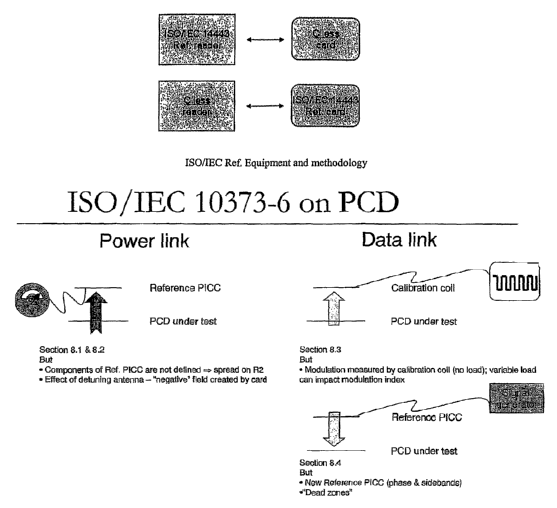
FIG. lb shows the functional tests conducted on a product reader
under ISO 10373-6 for testing the power and data links between cards and
readers.
While the separate card and reader compliance test procedures under
ISO 10373-6 may ensure that deployed product devices individually have
characteristics that fall in either the designated specification range for
cards or
readers, the procedures do not ensure interoperability in the field. Cards
and/or
readers verified as compliant may be only marginally so (e.g., by having a
characteristic value at the end or edge of a designated specification range).
This
manner of standards compliance can lead to operational failure in the field.
For
example, a marginally compliant card may be unreadable or difficult to read
using a
card reader that is also only marginally compliant.
Consideration is now being given to ways of enhancing
interoperability of electronic payment devices that are used in contactless
electronic
payment systems. Attention is directed to reducing variations in card and
reader
properties consistent with commonly accepted Standards. In particular,
attention is
directed to improving specification compliance procedures to enhance
interoperability.
SUMMARY OF THE INVENTION
In accordance with the present invention, methods and systems
are provided for enhancing interoperability of electronic payment devices that
are
used in contactless electronic payment systems. The electronic payment devices
include RFID-embedded cards issued to consumers and proximity coupling devices
such as RFID-enabled readers deployed by merchants. The methods and systems
involve use of a reference card and a reference reader to establish acceptable
specifications for issued cards and deployed readers, respectively. The
reference card
and reference reader are cross-calibrated to link the operational
specifications for the
cards and the readers. A suitable selection of overlapping specification
ranges or
tolerances for proper card and reader functions, then enhances the
interoperability of
the issued cards with a deployed reader, and also the interoperability of
deployed
readers with an issued card.
4
CA 02573814 2007-01-12
WO 2006/019997 PCT/US2005/025119
Further features of the invention, its nature and various
advantages will be more apparent from the accompanying drawings and the
following
detailed description.
BRIEF DESCRIPTION OF THE DRAWINGS
FIG. 1 a is a block diagram which schematically illustrates the use of a
Reference PICC for testing the properties of a product contactless payment
card
reader and the use of a Reference PCD for testing the properties of a product
contactless payment card, as prescribed by the ISO 10373-6 Standard.
F1G. lb is a schematic illustration of a set of functional tests
conducted on a product reader under conventional procedures for testing power
and
data links between cards and readers according to ISO 10373-6.
FIG. 2a is a block diagram, which schematically illustrates the step of
cross calibrating of a Reference PICC with a Reference PCD in accordance with
the
principles of the present invention. The cross-calibrated Reference PICC and
PCD
devices are then used for testing the functional properties and specifications
of a
product contactless payment card and reader, respectively.
F1G. 2b is a schematic illustration of the functional tests conducted on
a product reader for testing the power and data links between contactless
proximity
cards and readers in accordance with the principles of the present invention.
FIG. 3 is a graph illustrating a range of behaviors of diverse cards
simulated by a reference card and as measured or observed by a reference
reader, in
accordance with the principles of the present invention.
FIG. 4 is a graph illustrating the behavior of a complaint card whose
behavior lies in the range of behaviors observed in FIG. 3 in accordance with
the
principles of the present invention.
FIG. 5 is a graph illustrating the behavior of a reference card as
measured on a reference reader, relative to the behaviors shown in FIG. 3, in
accordance with the principles of the present invention.
FIG. 6 is a graph illustrating the behavior of a compliant card of FIG. 4
as measured on a calibrated reference reader, in accordance with the
principles of the
present invention.
5
CA 02573814 2007-01-12
WO 2006/019997 PCT/US2005/025119
FIG. 7 is a graph illustrating the overlapping specifications derived
form cross calibrated reference devices, in accordance with the principles of
the
present invention.
DETAILED DESCRIPTION OF THE INVENTION
The present invention is described in the context of implementations of
electronic payment systems in which the contactless payinent device
specifications
are intended to conform to a common industry standard such as the ISO 14443
Standard, which further specifies standardized test methods (i.e., ISO 10373 -
6 Test
Methods, Proximity Cards) for verification of the specification of individual
contactless payment devices. Recently, assignee MasterCard International
Incorporated ("MasterCard") has developed proprietary specifications
MasterCard
PayPassTM ISO/IEC 14443 Implementation Specification ("PayPass") for
implementation of proximity payment card technologies. The PayPass
implementation is consistent with the ISO 14443 Standard and provides a
convenient
example illustrating the principles of the present invention. It will be
understood that
the selection of the PayPass implementation for purposes of illustration is
only
exemplary, and that the principles of the present invention can be more
generally
applied to electronic payment devices and systems that operate under other
common
industry or proprietary standards.
The present invention provides a method and a system for enhancing
the interoperability of contactless payment devices (i.e., product cards
issued to
consumers and product readers deployed by merchants), which may be used to
conduct electronic payment transactions in the field. The system and method
ensure
that individual product cards and readers operate or function in tighter
specification
ranges than they are permitted to operate under the ISO 14443 standard. The
system
and method involve cross-calibrating the reference devices (i.e., the
Reference PICC
and Reference PCD devices) which are used to test specification compliance of
individual product readers and cards under the ISO 14443 and ISO 10373-6
standards.
(See FIG. 2a). The Reference PCD is used to establish a range of observed
functional
behaviors or parameters ("nominal card range") of the Reference PICC. Product
card
readers are required to have functional behaviors or parameters that are
within this
nominal card range as measured by the Reference PCD. Conversely, a Reference
6
CA 02573814 2007-01-12
WO 2006/019997 PCT/US2005/025119
PICC is used to establish a range of observed functional behaviors or
parameters
("nominal reader range") of Reference PCDs. Product readers are required to
have
functional behaviors or parameters that are within the nominal reader range
when
reading the reference card.
FIG. 2b schematically shows the functional tests conducted under the
PayPass implementations according to the present invention.
The cross-calibration of the Reference PICC and Reference PCD
establishes a relation between the two standard devices, and links the
specifications
for individual product cards with the specifications for product readers. This
avoids
interoperability failures that may arise under conventional unconnected or
separate
testing of card and reader specifications, for example, when the cards and
readers lie
at the extreme edges of their respective specification ranges that are allowed
under the
ISO 14443 standard.
The system and method (which are both collectively referred to as the
"PayPass implementation" herein) are based on a mathematical algorithm which
ensures interoperability of product payment devices upon the suitable
selection or
specification of device parameters.
To ensure proper functioning of a product reader (e.g., PCD R) with a
product card (e.g., PICC C), a PayPass - Reference PICC is used to generate a
range
of behaviors [f2(x), f3(x)] in a function f of variable x. The fu.nction f
may, for
example, be a magnetic field response as a function of distance. This range of
behaviors [f2(x), f3(x)] is observed on a PayPass - Reference PCD. See FIG. 3.
The PayPass implementation may require or specify that a product card
(i.e. PICC C) must display a behavior fc(x) that falls within the range of
established
card behaviors [f2(x), f3(x)] to be "compliant". The behavior fc(x) is
observed on the
PayPass - Reference PCD. See FIG. 4.
Further, the PayPass implementation may require or specify that a
product reader (i.e. PCD R) must function correctly with the PayPass -
Reference
PICC exhibiting a range of card behaviors [fl(x), f4(x)] as observed on the
PayPass -
Reference PCD to be "compliant". By requiring or specifying that the range of
card
behaviors [fl (x), f4 (x)] must include the range of card behaviors [f2(x),
f3(x)], i.e.
[f2(x), f3(x)] c: [fl(x), f4(x)],
7
CA 02573814 2007-01-12
WO 2006/019997 PCT/US2005/025119
the behavior fc(x) of the particular card (PICC C) under consideration is
necessarily
within the operating range [fl (x), f4 (x)] of the reader (PCD R). See FIGS. 5
and 6.
Accordingly, the product reader PCD R is expected to operate properly with the
product card (PICC C).
Similarly for ensuring proper functioning of a product card (e.g., PICC
C) with a product reader (e.g., PCD R), the PayPass - Reference PCD is used to
generate a range of reader behaviors [g2(y), g3(y)] for function g of a
variable y as
observed on the PayPass - Reference PICC. The PayPass implementation may
require or specify that a "compliant" reader PCD R should display a behavior
gc(y)
that falls within the established range [g2(y), g3(y)], where the behavior
gc(y) is
measured on the PayPass - Reference PICC. Further, the PayPass implementation
may require or specify that a product card (i.e. PICC C) rriust function
correctly with
the PayPass - Reference PCD exhibiting a range of reader behaviors [gl(x),
g4(x)] as
observed on the PayPass - Reference PICC. By requiring or specifying that the
range
of reader behaviors [gi (x), g4 (x)] should include the range of reader
behaviors
[g2(x), g3(x)], which is mathematically represented as:
[g2(x), g3(x)] c [gl(x), g4(x)],
the behavior gc(x) of the particular reader (PCD R) under consideration is
necessarily
within the operating range [gl (x), g4 (x)] of the card (PICC C). Accordingly,
the card
(PICC C) is expected to operate properly with the reader (PCD R).
As a tangible illustration of the mathematical algorithm described
above, it may be useful to consider the example of the power requirements for
activating a product PICC card. A PCD reader must provide or transmit a
certain
amount of power to a PICC to activate the card. Conversely, a product PICC
card
must work with a certain amount of power received from the PCD reader. In the
PayPass implementation, the power PC(d), which is delivered or transmitted by
a
product PCD reader, is measured as function of distance d on the PayPass -
Reference
PICC. The value of the power level PC (d) measured on the Pay Pass - Reference
PICC is required or specified to fall within a range of power levels
Rb,,power=
In the cross-calibration procedure, the PayPass - Reference PCD is
configured to generate different power levels which vary over a range RR.,
power= The
power levels generated by the PayPass - Reference PCD are calibrated with
respect to
8
CA 02573814 2007-01-12
WO 2006/019997 PCT/US2005/025119
the PayPass - Reference PICC, i.e., the range RR.,,po,er is a value measured
on the
PayPass - Reference PICC. In the procedure, the output of a signal generator
or
power source (e.g. a voltage source) feeding the PayPass - Reference PCD may
be
increased or decreased until suitable power levels RR,,pW, are reached as
observed on
the PayPass - Reference PICC. The mathematical requirement
Rtx,power c Rrx,power
ensures that a product PCD reader will properly power a product PICC card. See
FIG. 7.
More generally, the algorithm described above in [0026] -[0033]
leads to a system and method for ensuring or enhancing power, data transfer,
and
other functional interoperability of product contactless payment devices. This
system
and method may, for example, involve:
(a) measuring the power provided by a PCD on a Reference PICC,
(b) measuring data transmission (e.g., modulation depth, or other
signal parameters) on the Reference PICC,
(c) testing data reception (e.g., load modulation sensitivity) by a
PCD by generating different signals through the Reference PICC. The
PayPass - Reference PICC is first calibrated with respect to the
Reference PCD to determine the levels and characteristics of the
different signals generated by the Reference PICC, and
(d) measuring the data transmission by a PICC on the Reference
PCD, with the Reference PCD sending "average" value commands to
the PICC and with the Reference PCD providing an "average" power
level. Both the power level and the command characteristics produced
by the Reference PCD are calibrated with respect to the Reference
PICC,
(e) checking the data reception and power sensitivity of a PICC
using the Reference PCD, with the Reference PCD sending commands
with modulation characteristics and power levels at the border of the
tolerance interval or range Rrx. Again, for setting these extreme
values, the Reference PCD is calibrated with respect to the reference
PICC.
9
CA 02573814 2007-01-12
WO 2006/019997 PCT/US2005/025119
The system and method for enhancing interoperability are utilized, for
example, in the practice of the PayPass implementation specification. For
completeness of description, exemplary portions of the PayPass implementation
specification, which describe the electrical characteristics of the
contactless interface
(i.e. Radio frequency and Signal interface) between a PICC and PCD, are
reproduced
in Appendix A. The reproduced portions also include step-by-step procedures
for
cross-calibrating Reference PICC and PCD devices that are used for
characterizing
the power and data links between payment devices.
It will be understood that the foregoing is only illustrative of the
principles of the invention, and that various modifications can be made by
those
skilled in the art without departing from the scope and spirit of the
invention.
CA 02573814 2007-01-12
WO 2006/019997 PCT/US2005/025119
2 Radio Frequency Power and Signal
lnterface
This chapter specifies the electrical characteristics of the two types (Type A
and Type B)
of contactless interface supported by PayPass. The interface includes both
power and
bi-directional communication between a PICC and a PCD.
2.1 Introduction
...............................................................................
......................... 27
2.2 RF Power
...............................................................................
............................ 29
2.2.1 PCD Requirements for Power Transfer PCD to PICC
..................................... 29
2.2.2 PICC Requirements for Power Transfer PCD to PICC
.................................... 30
2.2.3 Influence of the PICC on the Operating Field
.................................................. 31
2.2.4 PCD Requirements for the Carrier Frequency f,,
.............................................. 31
2.2.5 PICC Requirements for the Carrier Frequency ~
............................................. 32
2.3 Signal Interface PCD to PICC
........................................................................... 33
2.3.1 Introduction
...............................................................................
....................... 33
2.3.2 PCD Requirements for Modulation PCD to PICC - Type A
........................... 33
2.3.3 PICC Requirements for Modulation PCD to PICC - Type A
.......................... 35
2.3.4 PCD Requirements for Modulation PCD to PICC - Type B
........................... 35
2.3.5 PICC Requirements for Modulation PCD to PICC - Type B
.......................... 37
2.4 Signal Interface PICC to PCD
........................................................................... 38
2.4.1 Introduction
...............................................................................
....................... 38
2.4.2 PICC Requirements for Load Modulation
........................................................ 39
2.4.3 PICC Requirements for Subcarrier Modulation - Type A
............................... 40
2.4.4 PICC Requirements for Subearrier Modulation - Type B
............................... 41
2.4.5 PCD Requirements for Modulation PICC to PCD
........................................... 42
11
CA 02573814 2007-01-12
WO 2006/019997 PCT/US2005/025119
2.1 Introduction
This chapter specifies the RF Power and Signal Interface requirements for the
PCD and PICC. All
the requirements included in this chapter are specified in function of the
PayPass reference
equipment. Each requirement is preceded by a measurement procedure describing
how to use the
PayPass reference equipment to validate the specific requirement. The
remainder of this section
explains the approach for writing the requirements.
A device, which can be a PCD or a PICC, is either transmitting or receiving. A
PCD transmits
power and data to a PICC and receives data from this PICC. A PICC receives
power as well as
data from a PCD and can transmit data to the PCD. The different configurations
for transmitting
and receiving for PCD and PICC are illustrated in Table 2.1.
Table 2.1-Configurations Transmit and Receive
PCD PICC
Transmit Receive Transmit Receive
Power
Data
For each device, the requirements related to transmission are such that the
value of a transmission
parameter must fall within a well defined range R,,, for this parameter. The
requiremenits on
reception are such that the receiver must properly work with the value of
different parameter
varying over a range R,., relevant for each parameter. For interoperability,
the ranges for
corresponding transmission and reception parameters are defined so that the
range R.,X is contained
within R,.. (sometimes denoted as Ru c R.. ).
Whether a device meets the transmission requirements is measured by means of
the receiver of the
appropriate PayPass reference equipment. E.g. whether the transmitter of a PCD
meets the
requirements is measured by means of the PayPass - Reference PICC. The quality
of the
transmitter of a PICC is measured on the PayPass - Reference PCD.
Example:
A PCD must provide a certain level of power to a PXCC. The power delivered by
the PCD is
measured on the PayPass - Reference PICC. The value of the power level
measured on the
PayPass - Reference PICC must fall within range R~ roW~r.
Whether a device meets the reception requirements, is measured by having the
transmitter of the
appropriate PayPass reference equipment create a range of values for a number
of parameters. E.g.
whether the receiver of a PCD meets the requirements, is measured by having
the PayPass -
Reference PICC sending out different levels of load modulation. The quality of
the receiver of a
PICC is verified by having the PayPass - Reference PCD sending out different
levels of
modulation.
In order to calibrate the transmitter of the PayPass reference equipment, the
receiver of the
matching PayPass reference equipment is used. E.g. the load modulation level
of the PayPass -
Reference PICC is calibrated with respect to the FayPass - Reference PCD. The
modulation level
of the PayPass - Reference PCD is calibrated with respect to the PayPass -
Reference PICC.
12
CA 02573814 2007-01-12
WO 2006/019997 PCT/US2005/025119
Example:
A PICC must work with a certain power level provided by a PCD. The PayPass -
Reference PCD
generates different power levels, varying over a range R,.,,Powcr= The power
level of the PayPass -
Reference PCD is calibrated with respect to the PayPass - Reference PICC. This
means that
Rr,,power is a value measured on the PayPass - Reference PICC and that the
power level of the
signal generator feeding the PayPass - Reference PCD is increased/decreased
until the correct
(voltage) level is reached on the PayPass - Reference PICC.
The power and data transmission characteristics of a PCD can be tested in
isolation as the PCD is a
master device. Testing the characteristics of a PICC cannot be done in
isolation, as a PICC is a
slave device, requiring stimulation from a PCD. For testing the transmission
characteristics, the
PICC will receive commands from the PayPass - Reference PCD. Signal parameters
will have an
'average' value within the range R,, allowed, thus maximizing the probability
of a response from
the PICC.
For both a PCD or a PICC, checking the data reception characteristics depends
on some kind of
acknowledgement of the device that the data was well received. For a PCD,
sending the next
command (=data transmission) in the overall flow implies that the response
from the PayPass -
Reference PICC is well understood. For a PICC, a response (= data
transmission) implies that the
command from the PCD is well understood.
For the remainder of the text, the verbiage "function properly" will be used
for a PCD sending the
next command, following a response created by the PayPass - Reference PICC.
The verbiage
"function properly" is also used for a PICC seciding a response to a command
generated by the
PayPass - Reference PCD
The approach explained above leads to the following for what concerns power
and data transfer:
= Power provided by a PCD is measured on the PayPass - Reference PICC.
= Data transmission by a PCD (modulation depth,...) is measured on the PayPass
- Reference
PICC.
= Data reception by a PCD (load modulation sensitivity) is tested by creating
different signals
through the PayPass - Reference PICC. To determine the levels and
characteristics of the
signal generated by the PayPass - Reference PICC, the PayPass - Reference PICC
is first
calibrated with respect to the PayPass - Reference PCD.
= Data transmission by a PICC is measured on the PayPass - Reference PCD, with
the PayPass
- Reference PCD sending 'average' value commands to the PICC and with the
PayPass -
Reference PCD providing an 'average' power level, Both the power level and.
the command
characteristics produced by the PayPass - Reference PCD are calibrated with
respect to the
PayPass - Reference PICC.
= Data reception and power sensitivity of a PICC are checked by means of the
PayPass -
Reference PCD, with the PayPass - Reference PCD sending commands with
modulation
characteristics and power levels at the border of the tolerance interval R,
Again, for setting
these extreme values, the PayPass - Reference PCD is calibrated with respect
to the PayPass
- Reference PICC.
13
CA 02573814 2007-01-12
WO 2006/019997 PCT/US2005/025119
2.2 RF Power
This section specifies the requirements for the power transfer from PCD to
PICC through the
electromagnetic field created by the PCD.
2.2.1 PCD Requirements for Power Transfer PCD to PICC
This section specifies the PCD requirement for the power transfer from PCD to
PICC. The PCD
creates an energizing RF field (the Operating Field) that enables the PICC to
power up. Table 2.2
describes the measurement procedure for the power transfer from PCD to PICC.
Table 2.2-Measurement of Power Transfer PCD to PICC (PCD Transmission)
Step '#' Action
Step I Regulate the PCD in such a way that it emits the carrier without any
modulation.
Regulation of the PCD is performed by means of the SDK as described in [7TA].
Step 2 Calibrate the PayPass - Reference PICC for power and data reception as
specified in annex
B.6. 1.
Step 3 Place the Pa,yPass - Reference PICC in the Operating Volume of the PCD.
The modulator
input (J2) of the PeryPass - Reference PICC must be disconnected.
Step 4 Measure the voltage Vov (DC) at J 1 of the PayPass - Reference PICC.
Requirements 2.1-Power Transfer PCD to PICC (PCD Transmission)
PCD
2.2.1.1 Within the Operating Volume, the PCD shall generate a DC voltage Vov
at J I of the PayPass -
Reference PICC. Refer to Annex A for the value of Vov.
14
CA 02573814 2007-01-12
WO 2006/019997 PCT/US2005/025119
2.2.2 PICC Requirements for Power Transfer PCD to PICC
This section specifies the PICC requirement for the power transfer from PCD to
PICC. Table 2.3
describes the measurement procedure to verify if the PICC functions properly
with the PayPass -
Reference PCD creating an Operating Field with field strength Hov.
Table 2.3-Measurement of Power Transfer PCD to PICC (PICC Reception)
Step # Action
Step I Calibrate the PayPass - Reference PCD for power transmission as
specified in annex B.S.1.
Step 2 Place the PayPass - Reference PICC in position (r=0, cp =0, z=4, 0-0)
of the Operating
Volume of the PayPass - Reference PCD. The modulator input {J2) of the PayPass
-
Reference PICC must be disconnected.
Step 3 Regulate the signal generator V of the PayPass - Reference PCD in such
a way that it
generates a voltage of Vpv,MIN at the output 11 of the PayPass - Reference
PICC (refer to
Annex A.2 and use for Vav,MiN the minimum value of Vc,v for the PICC). Remove
the
PayPass - Reference PICC from the Operating Volume of the PayPass - Reference
PCD.
Step 4 Calibrate the PayPass - Reference PCD for data transmission as
specified in annex B.5.2
using the modulation characteristics MOD A1 (for Type A) or MOD B1 (for Type
B).
Step 5 Place the PICC in the Operating Volume of the PayPass - Reference PCD
and send a valid
command to the PICC. If the PICC responds, then the PICC functions properly at
minimum
power level. Remove the PICC from the Operating Volume of the PayPass -
Reference
PCD.
Step 6 Place the PayPass - Reference PICC in position (r=0, (p-0, z=0, 8=0) of
the Operating
Volume of the PayPass - Reference PCD. The modulator input (J2) of the PayPass
-
Reference PICC must be disconnected.
Step 7 Regulate the signal generator V of the PayPass - Reference PCD in such
a way that it
generates a voltage of Vov,MAx (refer to section A.2 and use for Vov,MAX the
maximum value
of Vov for the PICC) at the output J1 of the PayPass - Reference PICC. Remove
the
PayPass - Reference PICC from the Operating Volume of the PayPass.- Reference
PCD.
Step 8 Calibrate the PayPass - Reference PCD for data transmission as
specified in annex B.5.2
using the modulation characteristics MOD A I(for Type A) or MOD B 1(for Type
B).
Step 9 Place the PICC in the Operating Volume of the PayPass- Reference PCD
and send a valid
command to the PICC. If the PICC responds, then the PICC functions properly at
maximum
power level.
Requirements 2.2-Power Transfer PCD to PICC (PICC Reception)
PICC
2.2.2.1 A PICC shall function properly within the Operating Volume when placed
in the position where
the PayPass - Reference PICC shows a DC voltage Vov at J 1. Refer to Annex A
for the value
of Vov.
CA 02573814 2007-01-12
WO 2006/019997 PCT/US2005/025119
2.2.3 Influence of the PICC on the Operating Field
Due to the electromagnetic coupling (i.e. mutual inductance) between the PICC
and PCD antennas,
the PICC changes the Operating Field created by the PCD when brought into the
Operating
Volume. The magnetic field strength within the Operating Volume will decrease
due to the extra
load caused by the PICC. This section lists the PICC requirement limiting the
maximum load a
PICC is allowed to have.
The load of a PICC is measured by the voltage drop AVov (= Vov,FREE AIR -
VOV,PiGC) at J2 of the
PayPass - Reference PCD caused by the presence of the PICC in the Operating
Volume as
described in Table 2.4.
Table 2.4--Measurement of the Influence of the PICC on the Operating Field
Step # Action
Step 1 Calibrate the PayPass - Reference PCD for power transmission as
specified in annex B.5. 1.
Step 2 Measure Vov,rRESAIR (peak to peak) at J2 of the PayPass - Reference
PCD.
Step 3 Place the PICC in the Operating Volume of the PayPass - Reference PCD
and measure
Vov,rrcc (peak to peak) at J2 of the PayPass - Reference PCD. AVov is defined
as
VOV,FREE AIR "' VOV,eICC-
Requirements 2.3-Influence of the PICC on the Operating Field
PICC
2.2.3.1 When placed in the Operating Volume of the PayPass - Reference PCD, a
PICC shall cause a
voltage drop AV at J2 of the PayPass - Reference PCD not greater than
AVov,MAX. AVov is
defined as V0V,FfCEEA1R' VOVeiCC- VOV,FREEAIR is the voltage (peak to peak)
measured at J2
when there is no PICC in the Operating Volume. Vov.rIcc is the valtage (peak
to peak)
measured at J2 after bringing the PICC in the Operating Volume of the PayPass -
Reference
PCD. Refer to Annex A for the value of QVov,MAx=
2.2.4 PCD Requirements for.the Carrier Frequency f.
This section specifies the PCD requirement for the frequency of the Operating
Field (i.e. the
carrier frequency fe) created by the PCD. Table 2.5 describes how to measure
fc.
Table 2.5--Measurement of Carrier Frequency fC (PCD Transmission)
Step # Action
Step 1 Calibrate the PayPass - Reference PICC for power and data reception as
specified in annex
B.6.1.
Step 2 Regulate the PCD in such a way that it emits the carrier without any
modulation.
Regulation of the PCD is performed by means of the SDK as described in [7TA].
Step 3 Place the PayPass - Reference PICC in the Operating Volume of the PCD.
The modulator
input (J2) ofthe PayPass - Reference PICC must be disconnected.
16
CA 02573814 2007-01-12
WO 2006/019997 PCT/US2005/025119
Step # Action
Step 4 Capture the signal at the output of the Calibration Coil of the PayPass
- Reference PICC.
Perform a frequency spectrum analysis of the signal and verify if the
frequency of the carrier
falls within f,, Afr.
Requirements 2.4-Carrier Frequency fc (PCD Transmission)
PCD
2.2.4.1 The frequency of the Operating Field (carrier frequency) provided by
the PCD shall be fc Af,
Refer to Annex A for the values of f. and M.
2.2.5 PICC Requirements for the Carrier Frequency fc
The section specifies the requirement that the PICC must function properly
with a carrier
frequency f, Qfc. Table 2.6 describes how to verify if a PICC functions
properly with a carrier
frequency fGt4,f,.
Table 2.6-Measurement of Carrier Frequency fc (PICC Reception)
Step # Action
Step 1 Calibrate the PayPass - Reference PCD for power transmission as
specified in annex B.5.1,
but adjust the carrier frequency of the PayPass - Reference PCD to fc-Aft.
Step 2 Calibrate the Pa,yPass - Reference PCD for data transmission as
specified in annex 5.5.2
using the modulation characteristics MOD Al (for Type A) or MOD BI (for Type
B).
~Step 3 Place the PICC in the Operating Volume of the PayPass - Reference PCD
and send a valid
command. If the PICC returns a response, then the PICC functions properly.
Step 4 Repeat Step 1, Step 2 and Step 3 but adjust the carrier frequency of
the PayPass - Reference
PCD to fa-h.[1fo.
Requirements 2.5--Carrier Frequency fc (PICC Reception)
P1CC
2.2.5.1 When placed in the Operating Volume of the Pa,yPass - Reference PCD, a
PICC shall function
properly at a carrier frequency f,, Afc.
17
CA 02573814 2007-01-12
WO 2006/019997 PCT/US2005/025119
2.3 Signal Interface PCD to .PICC
This section specifies the modulation methods used by Type A and Type B for
the communication
PCD to PICC. It deals with:
= The data transmission characteristics of the PCD
= The reception capabilities of the PICC to interpret the data transmission of
the PCD.
2.3.1 Introduction
The ISO/IEC 14443 standard defines two possible modulation types, called Type
A and Type B.
For communication from PCD to PICC, both Type A and Type B use Amplitude Shift
Keying
(ASK). The amplitude of the carrier is switched between H, and H2, creating a
"lower level" when
the field is at value H2. The requirements of the "lower level" as well as of
the envelope of the
carrier for the two modulation types of ISO/JEC 14443 are defined below.
2.3.2 PCD Requirements for Modulation PCD to PICC - Type A
Type A communication from PCD to PICC uses the modulation principle of ASK
100%. The
carrier is turned on and off, creating a "lower level" when turned off. In
practice, it will result in a
modulation index of 95% or higher. The "lower level" for Type A modulation is
referred to as
"pause" by jISO/IEC 14443-2]. Table 2.7 describes how to measure the Type A
modulation
characteristics of a PCD.
Table 2.7--Measurement of Modulation PCD to P1CC - Type A (PCD Transmission)
Step # Action
Step 1 Calibrate the PayPass - Reference PICC for power and data reception as
specified in annex
B.6.1.
Step 2 Place the PayPass - Reference PICC in the Operating Volume of the PCD.
The modulator
input (J2) of the PayPass - Reference PICC must be disconnected.
Step 3 Request the PCD to send a WUPA command. Regulation of the PCD is
performed by
means of the SDK as described in [71'A].
Step 4 Capture the WUPA signal sent by the PCD at the output of the
Calibration Coil of the
PayPass - Reference PICC and analyze the modulation characteristics.
For this section, V represents the envelope of the signal measured at the
output of the Calibration
Coil of the PayPass - Reference PICC, placed in the Operating Volume of the
PCD. V, is the
initial value measured immediately before any modulation is applied by the
PCD. V2, V3 and V4
are defined as follows:
V2 = põ,AV i(Refer to Annex A for the value of p,-,,A)
V3 = 0.6VI
V4 = 0.9V,
18
CA 02573814 2007-01-12
WO 2006/019997 PCT/US2005/025119
Requirements 2.6-Modulation PCD to PICC - Type A (PCD Transmission)
PCD
2.3.2.1 The PCD shall modulate the Operating Field in the Operating Volume in
such a way that the
signal measured at the output of the Calibration Coil of the PayPass -
Reference PICC has the
following characteristics (see also Figure 2.1):
= V shall decrease from V, to less than V2 in a time t, - t2.
= If V does not decrease monotonically, the time between a local maximum and
the time of
passing the same value before the local maximum shall be ts. This shall only
apply if the
local maximum is greater than V2.
= V shall remain less than V2 for a time t2.
= V shall increase monotonically to V3 in a time t4.
= V shall increase monotonically ta V4 or more in a time t3.
= Overshoots immediately following the rising edge shall remain within (I
Vou,p,)Vi
Refer to Annex A for the values oft1, t2, ta, t4, ts and Vpu,a
Figure 2.1-Lower Level - Type A
v <VOUAV
100% ~~--
90 /n V4
60% V3 ! 1~.Ilik 5% 0 2
t
5% ~{ ~
100 0 -- ~ t UIPJJM~Ml 11
Z ~ '~ t ~
~ pF--- ,
t~
19
CA 02573814 2007-01-12
WO 2006/019997 PCT/US2005/025119
2.3.3 PICC Requirements for Modulation PCD to PICC - Type A
This section lists the requirements for the reception capabilities of a PICC
of Type A. Table 2.8
describes how to verify if a PICC functions properly with the PayPass -
Reference PCD applying
Type A modulation characteristics at the border of the tolerance interval.
Table 2.8-Measurement of Modulation PCD to PICC - Type A(PICC Reception)
Step # Action
Step 1 Calibrate the PayPass - Reference PCD for power transmission as
specified in annex B.5. 1.
Step 2 Calibrate the PayPass - Reference PCD for data transmission as
specified in annex B.5.2
using the modulation characteristics MOD Al. Step 3 Place the PICC in the
Operating Volume of the PayPass - Reference PCD and send a valid
command to the PICC. If the PICC returns a response, then the PICC functions
properly.
Step 4 Repeat Step 2 and Step 3 for each set of modulation characteristics
defined in Table B. 11.
Requirements 2.7-=--Modulation PCD to PICC - Type A(P1CC Reception)
P1CC
2.3.3.1 When placed in the Operating Volume of the PayPass - Reference PCD, a
PICC of Type A
shall function properly provided the PayPass - Reference PCD applies valid
modulation
characteristics.
2.3.4 PCD Requirements for Modulation PCD to PICC - Type B
Type B communication from PCD to PICC uses the modulation principle of ASK
10%. The
amplitude of the carrier is reduced to create a "lower level" with a
modulation index mi. The
requirements on the "lower level" as well as on the envelope of the carrier
are defined below.
Table 2.9 describes how to measure the Type B modulation characteristics of a
PCD.
Table 2.9-Measurement of Modulation PCD to P1CC - Type B (PCD Transmission)
Step # Action
Step I Calibrate the PayPass - Reference PICC for power and data reception as
specified in annex
8.6.1. _
Step 2 Place the PayPass - Reference PICC in the Operating Volume of the PCD.
The modulator
input (J2) of the Pa,yPass - Reference PICC must be disconnected.
Step 3 Request the PCD to send a WUPB command. Regulation of the PCD is
performed by
means of the SDK as described in [TfA].
Step 4 Capture the WUPB signal sent by the PCD at the output of the
Calibration Coil of the
PayPass - Reference PICC and analyze the modulation characteristics.
CA 02573814 2007-01-12
WO 2006/019997 PCT/US2005/025119
For this section, V represents the envelope of the signal measured at the
output of the Calibration
Coil of the PayPass - Reference PICC, placed in the Operating Volume of the
PCD. V, is the
initial value measured immediately before any modulation is applied by the
PCD. V2 is the lower
level. The modulation index (mi), V3 and V4 are defined as follows:
- V~ - VZ
m; -
Vi + V2
V3 = Vi - 0.1(V!-VZ)
V4 = VZ+ 0.1(VrVz)
Requirements 2.8-Modulation PCD to PICC - Type B (PCD Transmission)
PCD
2.3.4.1 The PCD shall modulate the Operating Field in the Operating Volume in
such a way that the
signal measured at the output of the Calibration Coil of the PayPass -
Reference PICC has the
following characteristics (see also Figure 2.2):
= The modulation index (mi) of the signal shall be mod,.
= V shall decrease monotonically from V3 to Va in a time tf.
= V shall increase monotonically from V4 to V3 in a time tr.
= The rising and falling edges of the modulation shall be monotonic.
= Overshoots and undershoots immediately following the falling and rising edge
shall be less
than Vou,e(V i-Vz).
Refer to Annex A for the values of mod!, 4, tr and Vcu,s=
Figure 2.2- Modulation PCD to PICC - Type B
tr
V ; 4VOU,s(V1-y2) 4V0u,B(V1-V2)
V
t! V4
V2
,,,, + , ~ ~ ~=.
) =
01
iwt o ~lllu! k ;~
50%
100%[
21
CA 02573814 2007-01-12
WO 2006/019997 PCT/US2005/025119
2.3.5 PICC Requirements for Modulation PCD to PICC - Type B
This section lists the requirements for the reception capabilities of a PICC
of Type B. Table 2.10
describes how to verify if a PYCC functions properly when the PayPass -
Reference PCD applies
Type B modulation characteristics at the border of the tolerance interval.
Table 2.90----Measurement of PCD to PICC Modulation - Type B(P1CC Reception)
Step # Action
Step 1 Calibrate the PayyPass - Reference PCD for power transmission as
specified in annex B.5.1.
Step 2 Calibrate the PayPass - Reference PCD for data transmission as
specified in annex B.5.2
using the modulation characteristics MOD B 1.
Step 3 Place the PICC in the Operating Volume of the PayPass - Reference PCD
and send a valid
command to the PICC. If the PICC retum.s a response, then the PICC functions
properly.
Step 4 Repeat Step 2 and Step 3 for each set of modulation characteristics
defined in Table B.12.
Requirements 2.9-Modulation PCD to PICC - Type B(P1CC Reception)
PICC
2.3.5.1 When placed in the Operating Volume of the PayPass - Reference PCD, a
PICC of Type B
shall function properly, provided the PayPass - Reference PCD applies valid
modulation
characteristics.
22
CA 02573814 2007-01-12
WO 2006/019997 PCT/US2005/025119
2,4 Signal Interface PICC to PCD
This section specifies the modulation methods used by Type A and Type B for
the communication
PICC to PCD. It deals with:
= The data transmission characteristics of the PICC
= The reception capabilities of the PCD to interpret the data transmission of
the PICC.
2.4.1 Introduction
For the communication from PICC to PCD, both Type A and Type B cards use load
modulation.
The carrier frequency f. (13,56 MHz) is used to derive a subcarrier with
frequency f$ equal to f,,/16
(-847 kHz). The subcarrier is used to switch a load on and off. When the PICC
is in the loaded
state a higher current will flow through the antenna of the PICC than in the
case where the load is
not switched on. This difference in current in the PICC antenna is sensed by
the PCD.
Figure 2.3-Load Modulation
~
V , -7 ;--
~
Load Modulation '.~
.,. ,
100%
- ~ ~;
il
6
U' kE.
. t
100%
Type A cards modulate the subcarrier using On-Off Keying (OOK).
Type B cards modulate the subearrier using Binary Phase Shift Keying (BPSK), a
simple form of
Phase-Shift Keying (PSK). BPSK uses only two signal phases: 0 degrees and 180
degrees. If the
phase of the wave does not change with regards to a reference phase, then the
signal state stays the
same (low or high). If the phase of the wave changes by 180 degrees (i.e. the
phase reverses) then
the signal state changes. The reference phase is referred to as 00.
23
CA 02573814 2007-01-12
WO 2006/019997 PCT/US2005/025119
Figure 2.4-BPSK
v Phase Shift
10Q%
t
100% 2.4.2 PICC Requirements for Load Modulation
This section lists the load modulation requirements for the PICC. Table 2.11
describes how to
measure the load modulation characteristics of a PICC.
Table 2.11-Measurement of Load Modulation Characteristies (PICC Transmission)
Step # ' Action
Step 1 Calibrate the PayPass - Reference PCD for power transmission as
specified in annex B.5.1.
Step 2 Calibrate the Pa,yPass - Reference PCD for data transmission as
specified in annex B.5.2
using the modulation characteristics MOD A1(for Type A) or MOD B 1(for Type
B).
Step 3 Place the PICC in the Operating Volume of the PayPass- Reference PCD.
Step 4 Cancel the carrier on the CMR circuit of the PayPass - Reference PCD so
that the
remaining carrier level is 10 mV (or less) by tuning C9, C10, C11 and VR1
(refer to annex
B.4.2.5 for more details).
Step 5 Send a WUPA command to a PICC of Type A or a WUPB command to a PICC of
Type B.
Step 6 Capture the response from the PICC and measure the load modulation
(Vpp) at the output of
the CMR circuit of the PayPass - Reference PCD.
24
CA 02573814 2007-01-12
WO 2006/019997 PCT/US2005/025119
Requirements 2.10-Load Modulation Characteristics (PICC Transmission)
PICC
2.4.2.1 When put in the Operating Volume of the PayPass - Reference PCD, the
P1CC shall modulate
the Operating Field in such a way that the signal measured at the output of
the CMR circuit of
the PayPass - Reference PCD has the following characteristics:
= The frequency fs of the signal shall be f~/16.
= The amplitude (Vpp) of the signal shall be Vpp,a (peak to peak) for Type A
and Vpp,r; (peak
to peak) for Type B.
Refer to Annex A for the values of Vpp,n and VpP,a.
2.4.3 PICC Requirements for Subcarrier Modulation - Type A
This section lists the PICC requirements for the modulation of the subcarrier
for the
communication from PICC to PCD for Type A.
Requirements 2.11- Subcarrier Modulation - Type A(P1CC Transmission)
PICC
2.4.3.1 A PICC of Type A shall modulate the subcarrier using On-Off Keying
(OOK).
2.4.3.2 When modulating the subcarrier, a PICC of Type A shall only start the
modulation with a
defined phase relation to the subcarrier: that is on the rising or falling
edge of the subcarrier
(see Figure 2.5).
Figure 2.5---Start of Subcarrier Modulation - Type A
Modulallny Siqnal
F -1 -1 F] F
Modulated Subcarrkr
Start of Suboarrier
ModulaQan
Modulatinp Stpnat
ModulaNd Suburriv
Start of Subcarriar
Moduidion
CA 02573814 2007-01-12
WO 2006/019997 PCT/US2005/025119
2.4.4 PICC Requirements for Subcarrier Modulation - Type B
A PICC of Type B modulates the subcarrier using Binary Phase Shift Keying.
Before the PICC
sends information to the PCD by means of phase shifts, PICC and PCD first
establish a reference
phase 00. Then the PICC can start modulating the subcarrier: a change of logic
level is denoted by
a phase shift of 180 of the subearrier.
Requirements 2.12-Subcarrier Modulation - Type B(PICC Transmission)
PlCC
2.4.4.1 A PICC of Type B shall modulate the subcarrier using Binary Phase
Shift Keying.
2.4.4.2 A PTCC of Type B shall generate a subcarrier only when data is to be
transmitted.
2.4.4.3 Phase shifts shall only occur at nominal positions of rising or
falling edges of the subcarrier
(refer to Figure 2.6).
Figure 2.6-Allowed Phase Shifts - Type B
1 0 F] F] 11 FTI F] FL-0 [I F,
Phase change at nominai
position of the subcarder
26
CA 02573814 2007-01-12
WO 2006/019997 PCT/US2005/025119
2.4.5 PCD Requirements for Modulation PICC to PCD
This section lists the requirements for the reception capabilities of a PCD to
interpret the'
modulation applied by the PICC. Table 2.12 describes how to verify if a PCD
functions correctly
with the PayPass - Reference PICC applying modulation characteristics at the
border of the
tolerance interval.
Table 2.12-Measurement of Modulation PICC to PCD (PCD Reception)
Step # Action
Step I Calibrate the PayPass - Reference PICC for data transmission as
described in annex B.6.2
using the load modulation characteristics MOD LA 1.
Step 2 Place the PayPass - Reference PICC in the Operating Volume of the PCD.
Step 3 Request the PCD to send a valid command to the PayPass - Reference PICC
using Type A
modulation. Return a correct response by means of the PayPass - Reference
PICC. If the
PCD continues with the next valid command, then the PCD functions properly.
Step 4 Repeat Step 1, Step 2 and Step 3 for each set of load modulation
characteristics defined in
Table B.15.
Step 5 Calibrate the PayPass - Reference PICC for data transmission as
described in annex B.6.2
using the load modulation characteristics MOD I.B1.
Step 6 Place the PayPass - Reference PICC in the Operating Volume of the
PCD.~~~
Step 7 Request the PCD to send a valid command to the PayPass - Reference PICC
using Type B
modulation. Return a correct response by means of the PayPass - Reference
PICC. If the
PCD continues with the next valid command, then the PCD functions properly.
Step 8 Repeat Step 5, Step 6 and Step 7 for each set of load modulation
characteristics defined in
Table B.16.
Requirements 2.13-Modulation P1CC to PCD (PCD Reception)
PCD
2.4.5.1 The PCD shall function properly with the PayPass - Reference PICC
provided the PayPass -
Reference PICC applies valid load modulation characteristics.
27
CA 02573814 2007-01-12
WO 2006/019997 PCT/US2005/025119
B.5 Calibration of PayPass - Reference PCD
This annex describes how to configure the PayPass - Reference PCD to validate
the requirements
included in chapter 2.
B.5.1 Calibration of PayPass - Reference PCD for Power Transmission
Table B.9 describes how to calibrate the PayPass - Reference PCD for power
transmission.
Table B.9---Calibration of PayPass - Reference PCD for Power Transmission
Step # Action
Step I Calibrate the PayPass - Reference PICC as described in annex B.6.1.
Step 2 Tune the input impedance of the PayPass - Reference PCD to 50 SZ by
means of VC2.
Step 3 Tune the resonance frequency of the PayPass - Reference PCD to 13.56
MHz by means of
VC1.
Step 4 Place the PayPass - Reference PICC in the Operating Volume of the
PayPass - Reference
PCD at position (r=0, 9=0, z=4, 0=0).
Step 5 Connect input J1 of the PayPass - Reference PCD with a signal generator
V generating a
carrier signal with a frequency f, (13.56 MHz) measured at the output of the
Calibration
Coil of the PayPass - Reference PICC. Regulate the signal generator V in such
a way that
it generates a voltage of 2.3 V at the output J i of the PayPass - Reference
PICC (2.3 V
corresponds to :E600 mW (15.5 V at 50 S2) delivered at the PayPass- Reference
PCD
Antenna).
Step 6Remove the PrryPass - Reference PICC from the Operating Volume of the
PayPass -
Reference PCD.
B.5.2 Calibration of PayPass - Reference PCD for Data Transmission
Table B. 10 describes how to calibrate the PayPass - Reference PCD for data
transmission to a
PICC placed in the Operating Volume.
Table B.10-Calibration of PayPass - Reference PCD for Data Transmission
Step # Action
Step 1 Calibrate the PayPass - Reference PICC as described in annex B.6. 1.
Step 2 Place the PayPass - Reference PICC in the Operating Volume of the
Pa,yPass - Reference
PCD (at the same position as the position of the PICC during the measurement).
Step 3 Modulate the carrier to obtain one of the modulation characteristics
listed in Table B.1 I(for
Type A) or Table B. 12 (for Type B). The modulation characteristics are
measured at the
Calibration Coil output of the PayPass - Reference PICC.
Step 4 Remove the PayPass - Reference PICC from the Operating Volume of the
PayPass -
Reference PCD.
28
CA 02573814 2007-01-12
WO 2006/019997 PCT/US2005/025119
Table B.11 and Table B. 12 define the modulation characteristics used for Type
A and Type B.
Table B.11-Modulation Characteristics - Type A
Name ti (pause) p,n,A (lower value)
MODA1 2.6ps 4%
MOD A2 2.0 s 10%
Table B.12-Modulation Characteristics - Type B
Name m,
MOD B I 11 %
MOD B2 Refer to A.2 and use the minimum I'ICC value of modi.
MOD B3 Refer to A.2 and use the maximum PICC value of mod,.
B.G Calibration of PayPass - Reference PICC
This annex describes how to configure the PayPass - Reference PICC to validate
the requirements
included in chapter 2.
B.6.1 Calibration of PayPass - Reference PICC for Power and Data
Reception
Table B. 13 describes how to calibrate the PayPass - Reference PICC for power
and data
reception.
Table B.13-Calibration of PayPass - Reference P1CC for Power and Data
Reception
Step # Action
Step I Tune the resonance frequency of the PayPass -- Reference PICC to 16.1
MHz by means of
VC 1.
29
CA 02573814 2007-01-12
WO 2006/019997 PCT/US2005/025119
B.6.2 Calibration of PayPass - Reference PICC for Data Transmission
Table B. 14 describes how to calibrate the PayPass - Reference PICC for data
transmission.
Table B.14--Calibration of PayPass - Reference PICC for Data Transmission
Step # Action
Step I Calibrate the Pa,yPass - Reference PICC as described in annex B.6.1.
Step 2 Calibrate the PayPass - Reference PCD as described in annex B.5.1.
Step 3 Place the PayPass - Reference PiCC in the Operating Volume of the
PayPass - Reference
PCD (at the same position as that will be used in the Operating Volume of the
PCD during
the measurement).
Step 4 Connect the matching network to the Calibration Coil of the PayPass -
Reference PICC
(refer to Figure B.2). Connect a sine wave generator to JI of the matching
network with a
frequency of 13.57 MHz and an amplitude of (80 -15z) mV (peak to peak)
measured at the
output of the CMR circuit of the PayPass - Reference PCD (z represents the
distance in cm
above the landing plane).
Step 5 Connect a square wave generator to J2 of the PayPass - Reference PICC
with a frequency
of 847 KHz (fJ16). Regulate Va, in such a way that the square wave modulates
the carrier
with amplitude Vpp (peak to peak) measured at the output of the CMR circuit of
the PayPass
- Reference PCD. Vpp has one of the values listed in Table B. 15 for Type A or
Table B. 16
for Type B.
Step 6 Remove the Pa,yPass - Reference PICC from the Operating Volume of the
PayPass -
Reference PCD.
Table B. 15 specifies the different Type A load modulation characteristics
applied by the PayPass
- Reference PICC.
Table B.15---Load Modulation Characteristics - Type A
Name Vpp (mV)
MOD LA 1 45
MOD LA2 Refer to A.2 and use the minimum PCD value of Vpp,A.
MOD LA3 Refer to A.2 and use the maximum PCD value of Vpp,A.
Table B. 16 specifies the different Type B load modulation characteristics
applied by the Pa}lPass -
Reference PICC.
Table B.15---Load Modulation Characteristics -- Type B
Name Vpp (mV)
MOD LB1 45
MOD LB2 Refer to A.2 and use the minimum PCD value of Vpp,g.
MOD LB3 Refer to A.2 and use the maximum PCD value of Vpp,g.