Note: Descriptions are shown in the official language in which they were submitted.
4
CA 02578857 2007-03-02
1
DESCRIPTION
OVD INSPECTION METHOD AND INSPECTION APPARATUS
TECHNICAL FIELD
The present invention relates to an inspection method
and inspection apparatus for an OVD attached to a base
material such as a bank note, securities, merchandise coupon,
or card.
BACKGROUND ART
An OVD (Optical Variable Device) is a foil formed by
depositing a metal on a relief diffraction grating and has a
unique optical change function such as three-dimensional image
formation or color shift. The OVD is called a hologram or metal
foil. There are a sheet type OVD made by die-cutting a sheet,
a patch type OVD formed into a predetermined shape, and a
linear thread type OVD. The OVDs are attached to a partial or
entire surface of a valuable printed product such as a bank note,
securities, merchandise coupon, or credit card and used as one
of anti-counterfeit technologies because of their advanced
manufacturing methods.
A printed product with an OVD is manufactured by
attaching a sheet- or patch-type hologram to a base material by
transfer or press. A thread-type OVD is contained in a base
material as a watermark or attached into or onto a sheet
surface by transfer or press.
In manufacturing products with OVD, defects such as a
pinhole or peeling may occur upon attaching a hologram sheet
to a base material due to, e.g., a hologram sheet print error, a
transfer error to a base material, or maladjustment of machines.
OVD attachment state inspection is an important item of quality
control. It is necessary to remove a product with a defect as a
defective. However, the pattern observed on the diffraction
grating of an OVD changes depending on a slight change in the
incident angle of light because the diffraction grating has a
dependence on the wavelength and incident angle of light. It is
CA 02578857 2007-03-02
2
therefore impossible to inspect a stable OVD attachment state
under visible light. An inspection method or apparatus places a
printed product with an OVD, acquires its image by using a
camera, and executes comparison testing by displaying the
image on a monitor or printing the image.
An inspection apparatus is known, which reproduces,
captures, and inspects a hologram image of a holographic
printed product containing a holographic region and a print
region (e.g., patent reference 1).
A hologram position inspection method and apparatus are
also used as an inspection method and apparatus capable of
easily detecting an edge of a hologram and easily inspecting
whether the hologram is applied within a tolerance (e.g., patent
reference 2).
There also exist a hologram sheet inspection method and
apparatus capable of automatically accurately inspecting many
different kinds of holograms in a large quantity at once and
continuously for each of error items including chipping of a
sheet, hologram image misregistration, and unprinted areas,
repetitive printing, and misregistration of hologram sheets (e.g.,
patent reference 3).
Patent reference 1: Japanese Patent Laid-Open
No. 2000-187008
Patent reference 2: Japanese Patent No. 3095215
Patent reference 3: Japanese Patent Laid-Open
No. 2002-181718
DISCLOSURE OF INVENTION
In the inspection method of the above-described
inspection apparatus, the reflecting layer of a reflective
hologram strongly regularly reflects irradiation light from an
irradiation means. An image capturing means receives the
reflected light so that the image is discriminated on the basis of
the difference between the hologram region and other regions.
If an image of regularly reflected light of irradiation light is
captured, the image exhibits strong reflection at some parts
CA 02578857 2007-03-02
3
depending on the irradiation light amount. This may make it
impossible to extract a form defect such as a hologram edge or
pinhole because of blur.
In the above-described hologram position inspection
method and apparatus, the position of a hologram placed on a
transparent plate is inspected by arranging an inspection plate
such as a shielding plate so that diffraction occurs within the
position tolerance in the visible light range. That is, the OVD
pattern is extracted in the visible light range where a slight
change in the angle changes the pattern. For this reason, the
method and apparatus are not adaptable when the base
material with an OVD is a flexile medium such as a paper sheet
because it is readily influenced by fluttering, angle, and
undulation.
The above-described hologram sheet inspection method
and apparatus segment an image obtained by capturing a
hologram sheet into a number of blocks, and recognize a
defective portion formed on an edge of the design part of the
hologram sheet on the basis of a difference image obtained by
pattern matching between the captured image and a reference
image containing the minimum and maximum values of each
block. If the base material has a uniform flat surface, like a
plate-shaped card, the method and apparatus are suitably used
to extract an edge. However, the surface of a base material
such as a paper sheet to which the present invention is applied
readily undulates as compared to a card, and the angle changes
due to, e.g., slight fluttering that occurs during conveyance. It
is therefore difficult to extract a defect of an OVD form.
As described above, when a printed product with an OVD
is input in the visible light range, the glossy pattern of the OVD
changes as shown in Fig. 1A or 1B depending on a slight change
in the incident angle or the state of the print material. For this
reason, stable OVD inspection by form comparison such as
pattern matching is impossible because defect extraction
becomes unusable in accordance with the change in the glossy
pattern. In addition, the boundary between the print material
CA 02578857 2007-03-02
4
and the OVD becomes indistinct due to the change in the glossy
pattern. Hence, the process of extracting an OVD form from an
image line part of the printed pattern is complex.
It is an object of the present invention to provide an OVD
inspection method and inspection apparatus capable of causing
an optical device to inspect the position of an OVD and
attachment defects such as burrs, chipping, fractures, pinholes,
malformation, and perforation in an OVD without any influence
of a change in the pattern of the OVD image due to a change in
the angle caused by fluttering or undulation during conveyance
upon capturing the attachment state of the OVD attached to a
printed product of a base material such as a paper sheet, unlike
the conventional techniques.
According to the present invention, there is provided an
OVD inspection method of inspecting an OVD-attached to a base
material by using an inspection apparatus including illumination
means, image input means including image capturing means,
storage means, and image processing means, comprising:
arranging the image capturing means and the
illumination means at positions where mirror-reflected light and
diffracted light from a region of the OVD in a wave range not
less than 650 [nm] have values not more than a threshold value
upon a binarization process by the image processing means;
causing the illumination means to irradiate a surface of
the base material with infrared rays or light containing infrared
rays;
causing the image input means to input image data
including a wave range not less than 650 [nm] from a region
including the OVD attached to the base material;
causing the storage means to store, in advance,
reference image data of an OVD serving as a standard, or the
reference image data and reference data indicating a reference
position of the OVD serving as the standard; and
causing the image processing means to execute the
binarization process of the input image data, compare the
binarized image data with the reference image data, or the
CA 02578857 2007-03-02
binarized image data with the reference image data and the
reference data, and determine acceptability of at least one of a
form, area, and position of the OVD attached to the base
material on the basis of a comparison result.
5 According to the present invention, there is provided an
OVD inspection method of inspecting an OVD attached to a base
material by using an inspection apparatus including illumination
means, image input means including image capturing means,
storage means, and image processing means, comprising:
arranging the image capturing means and the
illumination means at positions where mirror-reflected light and
diffracted light from a region of the OVD in a wave range not
less than 650 [nm] have values not more than a threshold value
upon a binarization process by the image processing means;
causing the illumination means to irradiate a surface of
the base material with infrared rays or light containing infrared
rays;
causing the image input means to input image data
including a wave range not less than 650 [nm] from a region
including the OVD attached to the base material;
causing the storage means to store outline data
indicating an outline of an OVD serving as a standard in
advance; and
causing the image processing means to execute the
binarization process of the input image data, extract outline
data of the OVD attached to the base material from the image
data and compare the extracted outline data with the outline
data of the OVD serving as the standard, and determine
acceptability of a form of the OVD attached to the base material
on the basis of a comparison result.
Further, according to the present invention, there is
provided an OVD inspection method of inspecting an OVD
attached to a base material by using an inspection apparatus
including illumination means, image input means including
image capturing means, storage means, and image processing
means, comprising:
CA 02578857 2007-03-02
6
arranging the image capturing means and the
illumination means at positions where mirror-reflected light and
diffracted light from a region of the OVD in a wave range not
less than 650 [nm] have values not more than a threshold value
upon a binarization process by the image processing means;
causing the illumination means to irradiate a surface of
the base material with infrared rays or light containing infrared
rays;
causing the image input means to input image data
including a wave range not less than 650 [nm] from a region
including the OVD attached to the base material;
causing the storage means to store reference data
indicating an area value of an OVD serving as a standard in
advance; and
causing the image processing means to execute the
binarization process of the input image data, calculate an area
value of the OVD attached to the base material from the image
data and compare the calculated area value with the area value
indicated by the reference data of the OVD serving as the
standard, and determine acceptability of an attachment state of
the OVD on the basis of a comparison result.
Further, according to the present invention, there is
provided an OVD inspection method of inspecting an OVD
attached to a base material by using an inspection apparatus
including illumination means, image input means including
image capturing means, storage means, and image processing
means, comprising:
arranging the image capturing means and the
illumination means at positions where mirror-reflected light and
diffracted light from a region of the OVD in a wave range not
less than 650 [nm] have values not more than a threshold value
upon a binarization process by the image processing means;
causing the illumination means to irradiate a surface of
the base material with infrared rays or light containing infrared
rays;
causing the image input means to input image data
CA 02578857 2007-03-02
7
including a wave range not less than 650 [nm] from a region
including the OVD attached to the base material;
causing the storage means to store, in advance,
coordinates representing a position of an OVD and coordinates
indicating a reference position to detect the position of the OVD
when an OVD serving as a standard is attached to the base
material; and
causing the image processing means to execute the
binarization process of the input image data, calculate, from the
image data, coordinates indicating a position of the OVD
attached to the base material and a reference position to detect
the position of the OVD and compare the position of the OVD
attached to the base material and the reference position to
detect the position of the OVD with the coordinates representing
the position of the OVD and the coordinates indicating the
reference position to detect the position of the OVD when the
OVD serving as the standard is attached to the base material,
and determine acceptability of the position of the OVD on the
basis of a comparison result.
Further, according to the present invention, there is
provided an OVD inspection method of inspecting an OVD
attached to a base material by using an inspection apparatus
including illumination means, image input means including
image capturing means, storage means, and image processing
means, comprising:
arranging the image capturing means and the
illumination means at positions where mirror-reflected light and
diffracted light from a region of the OVD in a wave range not
less than 650 [nm] have values not more than a threshold value
upon a binarization process by the image processing means;
causing the illumination means to irradiate a surface of
the base material with infrared rays or light containing infrared
rays;
causing the image input means to input image data
including a wave range not less than 650 [nm] from a region
including the OVD attached to the base material and a reference
CA 02578857 2007-03-02
8
mark to detect a position of the OVD;
causing the storage means to store, in advance,
coordinates representing a position of an OVD and coordinates
representing a reference mark to detect the position of the OVD
when an OVD serving as a standard is attached to the base
material; and
causing the image processing means to execute the
binarization process of the input image data, calculate, from the
image data, coordinates representing a position of the OVD
attached to the base material and a position of the reference
mark and compare the coordinates representing the position of
the OVD attached to the base material and the position of the
reference mark with the coordinates representing the position of
the OVD and the coordinates representing the reference mark to
detect the position of the OVD when the OVD serving as the
standard is attached to the base material, and determine
acceptability of the position of the OVD on the basis of a
comparison result.
Further, according to the present invention, there is
provided an OVD inspection method of inspecting an OVD
attached to a base material by using an inspection apparatus
including illumination means, image input means including
image capturing means, storage means, and image processing
means, comprising:
arranging the image capturing means and the
illumination means at positions where mirror-reflected light and
diffracted light from a region of the OVD in a wave range not
less than 650 [nm] have values not more than a threshold value
upon a binarization process by the image processing means;
causing the illumination means to irradiate a surface of
the base material with infrared rays or light containing infrared
rays;
causing the image input means to input image data
including a wave range not less than 650 [nm] from a region
including the OVD attached to the base material and a portion
representing a position of the base material;
CA 02578857 2007-03-02
9
causing the storage means to store, in advance,
coordinates representing a position of an OVD and coordinates
representing the base material when an OVD serving as a
standard is attached to the base material; and
causing the image processing means to execute the
binarization process of the input image data, calculate, from the
image data, coordinates representing the OVD attached to the
base material and coordinates representing the base material
and compare the coordinates representing the OVD attached to
the base material and the coordinates representing the base
material with the coordinates representing the position of the
OVD and the coordinates representing the base material when
the OVD serving as the standard is attached to the base
material, and determine acceptability of the position of the OVD
on the basis of a comparison result.
According to the present invention, there is provided an
OVD inspection apparatus for inspecting an OVD attached to a
base material, comprising:
illumination means having a light source to irradiate the
base material with the OVD with light containing infrared rays;
image input means for inputting image data including a
wave range not less than 650 [nm] from a region including the
OVD attached to the base material irradiated with the light
containing infrared rays from said illumination means, said
image input means including image capturing means which is
arranged, relative to said illumination means, at a position
where mirror-reflected light and diffracted light from the region
of the OVD in a wave range not less than 650 [nm] have values
not more than a threshold value upon a binarization process by
image processing means;
storage means for storing, in advance, reference image
data of an OVD serving as a standard or the reference image
data and reference data indicating a reference position of the
OVD serving as the standard; and
image processing means for executing the binarization
process of the input image data, comparing the binarized image
CA 02578857 2007-03-02
data with the reference image data, or comparing the binarized
image data with the reference image data and the reference
data, and determining acceptability of at least one of a form,
area, and position of the OVD attached to the base material on
5 the basis of a comparison result.
According to the present invention, there is provided an
OVD inspection apparatus for inspecting an OVD attached to a
base material, comprising:
illumination means having a light source to irradiate the
10 base material with the OVD with light containing infrared rays;
image input means for inputting image data including a
wave range not less than 650 [nm] from a region including the
OVD attached to the base material irradiated with the light
containing infrared rays from said illumination means, said
image input means including image capturing means which is
arranged, relative to said illumination means, at a position
where mirror-reflected light and diffracted light from the region
of the OVD in a wave range not less than 650 [nm] have values
not more than a threshold value upon a binarization process by
image processing means;
storage means for storing outline data indicating an
outline of an OVD serving as a standard in advance; and
image processing means for executing the binarization
process of the input image data, extracting outline data of the
OVD attached to the base material from the image data and
comparing the extracted outline data with the outline data of
the OVD serving as the standard, and determining acceptability
of a form of the OVD attached to the base material on the basis
of a comparison result.
According to the present invention, there is provided an
OVD inspection apparatus for inspecting an OVD attached to a
base material, comprising:
illumination means having a light source to irradiate the
base material with the OVD with light containing infrared rays;
image input means for inputting image data including a
wave range not less than 650 [nm] from a region including the
CA 02578857 2007-03-02
11
OVD attached to the base material irradiated with the light
containing infrared rays from said illumination means, said
image input means including image capturing means which is
arranged, relative to said illumination means, at a position
where mirror-reflected light and diffracted light from the region
of the OVD in a wave range not less than 650 [nm] have values
not more than a threshold value upon a binarization process by
image processing means;
storage means for storing area data indicating an area of
an OVD serving as a standard in advance; and
image processing means for executing the binarization
process of the input image data, extracting area data of the
OVD attached to the base material from the image data and
comparing the area data with the area data of the OVD serving
as the standard, and determining acceptability of an attachment
state of the OVD attached to the base material on the basis of a
comparison result.
According to the present invention, there is provided an
OVD inspection apparatus for inspecting an OVD attached to a
base material, comprising:
illumination means having a light source to irradiate the
base material with the OVD with light containing infrared rays;
image input means for inputting image data including a
wave range not less than 650 [nm] from a region including the
OVD attached to the base material irradiated with the light
containing infrared rays from said illumination means, said
image input means including image capturing means which is
arranged, relative to said illumination means, at a position
where mirror-reflected light and diffracted light from the region
of the OVD in a wave range not less than 650 [nm] have values
not more than a threshold value upon a binarization process by
image processing means;
storage means for storing, in advance, coordinate data
indicating coordinates representing a position of an OVD and
coordinates indicating a reference position to detect the position
of the OVD when an OVD serving as a standard is attached to
CA 02578857 2007-03-02
12
the base material; and
image processing means for executing the binarization
process of the input image data, calculating, from the image
data, coordinates indicating a position of the OVD attached to
the base material and a reference position to detect the position
of the OVD and comparing the position of the OVD attached to
the base material and the reference position to detect the
position of the OVD with the coordinates representing the
position of the OVD and the coordinates indicating the reference
position to detect the position of the OVD when the OVD serving
as the standard is attached to the base material, and
determining acceptability of the position of the OVD attached to
the base material on the basis of a comparison result.
According to the present invention, there is provided an
OVD inspection apparatus for inspecting an OVD attached to a
base material, comprising:
illumination means having a light source to irradiate the
base material with the OVD with light containing infrared rays;
image input means for inputting image data including a
wave range not less than 650 [nm] from a region including the
OVD attached to the base material irradiated with the light
containing infrared rays from said illumination means, said
image input means including image capturing means which is
arranged, relative to said illumination means, at a position
where mirror-reflected light and diffracted light from the region
of the OVD in a wave range not less than 650 [nm] have values
not more than a threshold value upon a binarization process by
image processing means;
storage means for storing, in advance, coordinate data
indicating coordinates representing a position of an OVD and
coordinates representing a position of a reference mark to
detect the position of the OVD when an OVD serving as a
standard is attached to the base material; and
image processing means for executing the binarization
process of the input image data, calculating, from the image
data, coordinates representing a position of the OVD attached to
CA 02578857 2007-03-02
13
the base material and the coordinates of a position of the
reference mark and comparing the coordinates representing the
position of the OVD attached to the base material and the
coordinates representing the position of the reference mark with
the coordinates of a position representing the OVD and the
coordinates representing the position of the reference mark to
detect the position of the OVD when the OVD serving as the
standard is attached to the base material, and determining
acceptability of the position of the OVD attached to the base
material on the basis of a comparison result.
According to the present invention, there is provided an
OVD inspection apparatus for inspecting an OVD attached to a
base material, comprising:
illumination means having a light source to irradiate the
base material with the OVD with light containing infrared rays;
image input means for inputting image data including a
wave range not less than 650 [nm] from a region including the
OVD attached to the base material irradiated with the light
containing infrared rays from said illumination means, said
image input means including image capturing means which is
arranged, relative to said illumination means, at a position
where mirror-reflected light and diffracted light from the region
of the OVD in a wave range not less than 650 [nm] have values
not more than a threshold value upon a binarization process by
image processing means;
storage means for storing, in advance, coordinate data
indicating coordinates representing a position of an OVD and
coordinates representing a position of the base material when
an OVD serving as a standard is attached to the base material;
and
image processing means for executing the binarization
process of the input image data, calculating, from the image
data, coordinates representing a position of the OVD attached to
the base material and coordinates of a position representing the
base material and comparing the coordinates representing the
position of the OVD attached to the base material and the
= CA 02578857 2007-03-02
14
coordinates of the position representing the base material with
the coordinates of a position representing the OVD and the
coordinates of the position representing the base material when
the OVD serving as the standard is attached to the base
material, and determine acceptability of the position of the OVD
attached to the base material on the basis of a comparison
result.
Here, in the above OVD inspection method, said
illumination means and said image capturing means may be
arranged such that
an angle ~ between said illumination means and said
image capturing means,
a wavelength a, [nm] of the light emitted from said
illumination means, and
the number N (N >_ 1) of trenches per 1 [mm] in the OVD
hold a relationship given by sin4 < NX [nm] x 10"6 in the region
of the OVD attached to the base material.
In the above OVD inspection apparatus, said illumination
means and said image capturing means may be arranged such
that
an angle 4. between said illumination means and said
image capturing means,
a wavelength X. [nm] of the light emitted from said
illumination means, and
the number N (N >_ 1) of trenches per 1 [mm] in the OVD
hold a relationship given by sin4 < NA, [nm] x 10-6 in the region
of the OVD attached to the base material.
The surface of the applied OVD is considerably flat.
Reflected light contains a mirror-reflected light component and a
diffracted light component. In acquiring the image of the OVD
region, when the influence of mirror-reflected light and
diffracted light from the OVD is eliminated, the contrast of
infrared transmitting characteristic from the printed product
around the OVD can be used. In this way, the form of the OVD,
partial defects, and position accuracy can be evaluated.
Especially even when the printed product with the OVD is
CA 02578857 2007-05-29
conveyed at a high speed, and the print base material slightly floats,
flutters,
or undulates during conveyance, it is possible to always stably acquire the
image data of the OVD form by using infrared rays that hardly generate
diffracted light as compared to visible light. Hence, online complete
5 inspection of OVD attachment quality can be done accurately.
Even in a resting state, it is possible to input and inspect the image
data of the OVD.
The present invention is applicable not only to a stripe- and patch-type
holograms but also to a thread-type hologram.
10 BRIEF DESCRIPTION OF THE DRAWINGS
Figs. 1(a) to 1(d) are explanatory views showing images of a printed
product with an OVD which are acquired in the visible light range;
Figs. 2 (a) to 2(c) are explanatory views showing printed products with
different OVDs;
15 Fig. 3 is a schematic view showing the arrangement of an apparatus
for inspecting an OVD offline according to the embodiment of the present
invention;
Fig. 4 is an explanatory view showing the angle between diffracted
light and incident light with a wavelength A to a diffraction grating;
Fig. 5 is a graph showing an example of the spectral sensitivity of a
CCD area sensor camera used in the OVD inspection apparatus according to
the embodiment;
Fig. 6 is a graph showing an example of the spectral sensitivity of a
CCD line sensor camera used in the OVD inspection apparatus according to
the embodiment;
Fig. 7 is a graph showing the spectral transmittance of a visible light
cutting infrared transmitting filter in the OVD inspection apparatus according
to the embodiment;
Figs. 8(a) to 8(d) are explanatory views showing images of a printed
product with an OVD which are acquired in the infrared range;
Fig. 9 is an explanatory view showing the relationship
CA 02578857 2007-05-29
16
between the wavelength and the reflection angle when light that has entered
the diffraction grating is reflected;
Figs. 10(a) to 10(g) are explanatory views showing examples of binary
images representing defects obtained in the embodiment;
Figs. 11(a) to 11(g) are explanatory views showing examples of
images representing the outlines of defects obtained in the embodiment;
Fig. 12 is a flowchart showing a process of executing OVD attachment
inspection according to the embodiment;
Fig. 13 is a block diagram showing the arrangement of an image input
means, image processing means, storage means, and output means
included in the OVD inspection apparatus according to the embodiment;
Fig. 14 is a flowchart showing a process of inspecting an OVD offline
according to the embodiment;
Figs. 15(a) and 15(b) are explanatory views showing a method of
measuring an OVD attachment position according to the embodiment;
Fig. 16 is a schematic view showing the arrangement of an inspection
apparatus for inspecting an OVD online according to the embodiment;
Fig. 17 is a flowchart showing a process of inspecting an OVD online
according to the embodiment;
Fig. 18 is a schematic view showing the arrangement of a light source
and a camera upon inspecting an OVD online according to the embodiment;
and
Fig. 19 is an explanatory view showing a printed product by
photocomposing to which a plurality of OVDs are attached.
DESCRIPTION OF THE REFERENCE NUMERALS
1 CCD area sensor camera with visible light cutting infrared transmitting
fitter
2 light source
3 printed product
4 OVD
5, 12 image input means
CA 02578857 2007-03-02
17
6, 13 image processing means
6a calculation unit
6b determination unit
7 CCD line sensor camera with visible light cutting infrared
transmitting filter
8 linear light source
9 inspection cylinder
10, 20 input unit
14 reference mark
15 pattern on surface of printed product
21 output means
22 storage means
BEST MODE FOR CARRYING OUT THE INVENTION
An embodiment of the present invention will be
described.
An OVD inspection method and apparatus according to
the embodiment can inspect, e.g., any one of a patch-type OVD
4a attached onto a base material 1 of a printed product 3 as
shown in Fig. 2(a), a stripe-type OVD 4b as shown in Fig. 2(b),
and a thread-type OVD 4c as shown in Fig. 2(c).
Preferably, the OVD is a printed pattern using infrared
transmission ink or is attached onto a base material that reflects
infrared rays so that the image of the OVD can. be acquired
more clearly.
To inspect the OVD 4 attached to the printed product 3,
the inspection apparatus used to execute the OVD inspection
method according to the embodiment comprises an image input
means 5 including a camera 1 serving as an image capturing
means and an input unit 10 which inputs image data captured
by the camera 1, a light source 2 serving as an irradiation
means, and an image processing means 6 for executing a
predetermined process for received image data, as shown in
Fig. 3.
The camera 1 is an image capturing means. A CCD area
sensor camera with a visible light cutting infrared transmitting
CA 02578857 2007-03-02
4
18
filter which removes the visible light range with a wavelength
shorter than 650 [nm] and transmits the infrared range with a
wavelength of 650 [nm] or more is used.
The camera 1 is preferably arranged perpendicular to an
inspection target, i.e., an OVD 4 to avoid any distortion in its
image.
The light source 2 is an illumination means. The light
source 2 preferably irradiates the OVD 4 obliquely because
mirror-reflected light from the region of the OVD 4 must not
largely influence the camera 1. More specifically, the
mirror-reflected light must have a predetermined light intensity
or less. The light source 2 is installed at such a position that
the mirror-reflected light obtains a threshold value or less upon,
e.g., a binarization process by the image processing means 6.
However, if the irradiation direction is too close to a direction
parallel to the OVD 4, the light-receiving amount decreases.
The light source 2 needs to be installed in consideration of this
as well.
It is also indispensable to set the light source 2 at such a
position that diffracted light generated from the OVD 4 rarely
affects the camera 1. The power of diffracted light generated
from the OVD 4 has directivity. Hence, it is preferable to
arrange the light source 2 with respect to the inspection target,
i.e., the OVD 4 to minimize the diffracted light. To prevent the
camera 1 from receiving the diffracted light from the OVD 4 as
much as possible, the light intensity of the diffracted light must
have a predetermined value or less, and for this purpose, the
light source 2 is installed at such a position that the diffracted
light obtains a threshold value or less upon, e.g., a binarization
process by the image processing means 6.
Alternatively, the diffraction grating of the OVD 4, i.e.,
the inspection target and the camera 1 need to be arranged
such that a relationship given by sink < N2 x 10-6 holds, where 0
is the angle of incident light from the light source 2, 2, is the
wavelength of the incident light, and N (N >_ 1) is the number of
trenches per 1 [mm] in the diffraction grating, as shown in
CA 02578857 2007-03-02
19
Fig. 4. In addition, it is essential to arrange the light source 2
in a direction to inhibit the light source 2 from receiving
mirror-reflected light, as described above.
Examples of the camera 1 is a CCD line sensor camera
and a CCD area sensor camera. As a functional characteristic,
the camera 1 must have a relatively high spectral sensitivity in
the infrared range with a wavelength of 650 [nm] or more as
shown in Fig. 5 or 6.
A CCD line sensor camera is suitable for capturing the
image of the OVD 4 during conveyance of the printed product 3.
One-dimensional images of a region including the OVD 4
attached to the printed product 3 are sequentially acquired by a
CCD line sensor camera, thereby generating a two-dimensional
image.
On the other hand, a CCD area sensor camera capable of
capturing a two-dimensional image is suitable for image
capturing of the printed product 3 at rest.
The camera can have, at its lens portion, a filter which
removes visible light with a wavelength shorter than 750 [nm]
and passes light in the infrared range with a wavelength of 750
[nm] or more, as shown in Fig. 7.
This makes it possible to cut reflected light in the visible
light range so as to avoid any change in the image related to
the form of the OVD 4 and acquire stable image data, as shown
in Fig. 8(a) or 8(b).
Almost the same effect is available by using a filter which
removes light in a wave range shorter than not 750 [nm] but
650 [nm] and a range of 650 [nm] or more.
An OVD image obtained by capturing the region including
the OVD 4 attached to the printed product 3 is a monochrome
image that is very useful for inspecting the OVD attachment
state, as shown in Fig. 8(c) or 8(d), unlike an image obtained
using visible light, i.e., a reflected image with a changeable OVD
surface. This image facilitates extraction of an OVD edge or
form. Hence, it is easy to extract and confirm attachment
defects such as burrs, chipping, fractures, pinholes,
CA 02578857 2007-03-02
malformation, and perforation.
The method and principle of OVD image data acquisition
will be described in more detail. Conventional image data
acquisition using visible light is suitable for acquiring a changing
5 pattern image in an OVD because reflected light from the OVD
is used. However, this technique is inappropriate for quality
inspection in manufacturing, i.e., checking the quality and
position during the process of attaching an OVD to a printed
product using a flexible medium such as a paper sheet as a
10 base material. For example, when image data in the region
including the OVD is acquired by using light in the visible light
range, the image shown in Fig. 1(a) is obtained, as described
above. Fig. 1(b) shows an image obtained by changing the
pattern in the OVD by changing the angle of the same OVD
15 region.
As is apparent from Figs. 1(a) and 1(b), even in a single
OVD with a certain design, captured image data changes
depending on the reflection of visible light because the pattern
image in the OVD changes.
20 When the acquired OVD images undergo binarization as a
general image process, images shown in Figs. 1(c) and 1(d) are
obtained. In binarization, a target is extracted from an image,
and the background and graphic pattern are separated to
analyze the characteristic feature of the image. More
specifically, a grayscale image with a density value is converted
into an image expressed by two values, 0 and 1. The images
shown in Figs. 1(c) and 1(d) are obtained by replacing bright
portions with white and dark portions with black by the
binarization process.
An auxiliary line indicated by a broken line represents the
OVD edge of the OVD region. These images are obtained by
executing the binarization process for the same OVD whose
internal pattern has changed due to a change in the observation
angle or illumination angle.
Even in the same OVD, the resultant images shown in
Figs. 1(c) and 1(d) exhibit different patterns in the visible light
CA 02578857 2007-03-02
21
range as if they were acquired from different OVDs. If strong
reflection takes place at the boundary between the OVD and the
paper surface, some kinds of changeable pattern images make
it very difficult to determine whether the image obtained by
reflection represents an OVD edge or discontinuity caused by
chipping, as shown in Fig. 1(d).
If the base material with the OVD is a card, image data
can be obtained by strictly setting the angle and position of the
camera and irradiation. However, if a paper sheet as a flexible
medium is irradiated with a light source in the visible light range,
slight fluttering during conveyance changes the angle, and in
turn, the exhibited image even when the light source position
does not change. This method is therefore inappropriate for
inspection.
In this embodiment, the region including the OVD is
irradiated with infrared rays or illumination containing infrared
rays, and an image is extracted. If the region is irradiated with
infrared rays or illumination containing infrared rays from a
direction to minimize the influence of mirror-reflected light and
diffracted light, a clear OVD image can be extracted because of
the contrast under the infrared rays.
In many cases, an OVD has a plurality of diffraction
directions. This limits the irradiation angle of illumination to
the camera and inspection target. In the diffraction grating of
an OVD, the reflection angle of visible light has a range a in
Fig. 9. On the other hand, the reflection angle of infrared rays
has a range 0 outside the angle range a.
If infrared rays irradiate a printed product surface with an
OVD, diffuse reflection occurs in all ranges a, 03, and 0 shown in
Fig. 9. Hence, the irradiation angle from the light source and
the camera position are set in consideration of the reflection
characteristic of the diffraction grating while irradiating the OVD
including region of the printed product with the OVD with
illumination containing infrared rays from the light source.
Then, the image of the vicinity of the region including the OVD
is captured.
CA 02578857 2007-03-02
s
22
Let N be the number of trenches per 1 [mm] in the OVD
portion where diffraction takes place. To prevent the camera
from receiving reflected light with the diffraction wavelength X
[nm] or more, the angle c~ made by the irradiation angle of
illumination and the light-receiving angle of the camera shown
in Fig. 4 must satisfy
sin4 < NX [nm] x 10"6 (1)
for all OVD regions, as described above.
Assume that the number of trenches per 1 [mm] in the
OVD is 500, and the wavelength is 750 [nm] or more. When
they are substituted into inequality (1), 4. < 49 . That is, the
angle the light-receiving angle of the camera makes with the
irradiation angle of the light source is preferably 490 or less with
respect to the printed product with the OVD. However, the
light source and camera need to be arranged in consideration of
the possibility that the camera may receive mirror-reflected
light if the angle 0 is too small.
For example, the camera for image data acquisition is
arranged immediately above the printed product. A filter is
attached to the lens portion of the camera. Image data is
extracted by irradiating the printed product with illumination
containing infrared rays at an angle of 30 with respect to the
camera. Since the image data is acquired in the angle range a
shown in Fig. 9, the camera receives the infrared rays reflected
by the paper surface of the printed product so that bright image
data is acquired. However, the OVD is captured as a dark
image because it does not reflect infrared rays.
The reflection angle in the range a shown in Fig. 9
changes depending on the inspection target. It is therefore
necessary to set the optimum position for each inspection target.
The obtained image data is displayed as a monochrome image
and subjected to a binarization process as normal image
processing. Then, the OVD is extracted as a black image,
whereas the paper surface of the printed product is extracted as
a white image.
If abnormalities such as chipping or pinholes are present
CA 02578857 2007-03-02
23
on the edge of the OVD or in it, they are captured white, as
shown in Figs. 10(a) to 10(g) because the infrared rays are
reflected even toward the camera, unlike the usual method.
When the edge (outline) of the OVD is extracted from the
obtained binary image, as shown in Figs. 11(a) to 11(g), the
subsequent process is easy. It is very useful because
comparison between the image data and standard image data
facilitates determination of the presence/absence of defects. A
printed product with defects detected is rejected.
As described above, this embodiment has as its primary
object to extract image data to recognize the form after OVD
attachment to the printed product. This embodiment does not
assume image acquisition to check the change state of the
pattern image by the diffraction grating in the OVD. To
optically acquire images of an OVD and a printed product with it,
a wave range of 650 [nm] or more is used.
In this embodiment, for example, an incandescent lamp
is selected as the light source containing infrared rays for the
inspection target, i.e., the OVD including region of the printed
product with the OVD. Alternatively, the light source is
appropriately selected from, e.g., an infrared LED (infrared
diode) and an infrared lamp which emit only infrared rays, and a
halogen lamp, sunlight, and an HID (High Discharge Lamp)
which emit light containing infrared rays.
Light emitted from such a light source and reflected by
the region including the OVD contains the visible light range and
ultraviolet range which are unnecessary for inspection. Only
the infrared range and longer wave range can be extracted by
attaching, to the lens portion of the camera, a filter which cuts
the visible light range and shorter wave range and transmits the
infrared range and longer wave range.
The camera used for image capturing is preferably a CCD
area sensor camera or CCD line sensor camera having a high
spectral sensitivity in the infrared range. The CCD area sensor
camera is suitable for image capturing in so-called offline
inspection wherein an inspection target is temporarily taken out
CA 02578857 2007-03-02
24
from the production line and inspected in a resting state on, e.g.,
an inspection stage on a table. On the other hand, the CCD
line sensor camera is suitable for image capturing in so-called
online inspection wherein an inspection target in a running state
is inspected on the production line during conveyance through
the attachment machine.
The image captured by the camera such as a CCD area
sensor camera or CCD line sensor camera is extracted as image
data of a two-dimensional image.
The extracted image data is input to the image input
means, sent to a memory held in the image processing means,
and temporarily stored. The memory stores reference image
data of an OVD serving as a standard in advance. Pattern
matching with the image data, comparison/determination of the
area, or OVD position extraction and comparison/determination
is done on the basis of the reference image data, thereby
determining the quality related to the form, area, and position
of the attached OVD.
The OVD is inspected in accordance with the procedure
shown in Fig. 12. If each item falls within the tolerance, the
OVD is determined as normal so that the printed product is
handled as a normal product. The printed product obtains a
number and undergoes, e.g., cutting. If an item falls outside
the tolerance, the OVD is determined as defective, so that the
printed product is discarded as a defective product.
Examples
Examples of the OVD inspection apparatus according to
the embodiment of the present invention will be described below
in more detail with reference to the accompanying drawings.
These are merely examples, and the present invention is not
limited to them.
(Example 1)
To inspect a printed product with an OVD in a resting
state and check the quality such as the OVD attachment state
offline, an OVD inspection apparatus having the arrangement
shown in Fig. 3 is used.
CA 02578857 2007-03-02
a
The OVD inspection apparatus has, as main components,
a light source 2, an image input means 5 including a CCD area
sensor camera (to be referred to as a CCD area sensor camera
hereinafter) 1 with a visible light cutting infrared transmitting
5 filter and an input unit 10, and an image processing means 6.
More specifically, as shown in Fig. 13, the image
processing means 6 includes an operation unit 6a that executes
various kinds of operations, and a determination unit 6b that
determines the quality by comparing the image data of an
10 inspection target with reference image data about a standard
OVD. The image processing means 6 also connects to a
storage means 22 for storing reference image data given in
advance and the given image data of an inspection target, and
an output means 21 for displaying an image or outputting a
15 warning upon receiving a comparison/determination result.
A printed product 3 as an inspection target with an OVD
4 is fixed on an offline inspection stage. As the light source 2
of irradiation, an incandescent lamp capable of emitting light
containing infrared rays is used. The light source 2 is set to an
20 irradiation angle of 30 with respect to the CCD area sensor
camera 1.
The CCD area sensor camera 1 has a filter to cut (shield)
a wave range shorter than 750 [nm] and transmit a wave range
of 750 [nm] or more as shown in Fig. 7. The CCD area sensor
25 camera 1 and the light source 2 relative to the attached OVD
are preferably arranged such that diffracted light from the OVD
4 does not enter the CCD area sensor camera 1.
The installation angle of the CCD area sensor camera 1
and light source 2 with respect to the OVD 4 is set such that the
irradiation angle becomes, e.g., 30 to prevent the lens of the
CCD area sensor camera 1 from receiving infrared rays reflected
by the OVD 4 on the printed product 3 with the OVD 4. Any
angle other then 30 can be set if it prevents mirror-reflected
light from entering the camera 1.
The OVD inspection process of the OVD inspection
method and apparatus according to Example 1 will be described
r
CA 02578857 2007-03-02
26
with reference to the flowchart in Fig. 14.
The printed product 3 as the inspection target with the
OVD 4 is irradiated with light containing infrared rays from the
light source 2 (S10).
As the irradiation light, light containing infrared rays, and
more preferably, light in the near infrared range of 750 [nm] to
1,100 [nm] suffices. An infrared lamp that emits only light in
the infrared range is more preferable, though the infrared lamp
is expensive. A more inexpensive and versatile light source
such as an incandescent lamp may be used in consideration of
the cost. In this case, unwanted light components can be
removed when the camera 1 acquires light transmitted through
the visible light cutting infrared transmitting filter. This
provides a wide choice of light sources. Hence, any light
source capable of emitting light containing infrared rays can be
used without any problem even when the visible light range
shorter than 750 [nm] and other wave ranges are included.
The CCD area sensor camera 1 captures the light in the
infrared range reflected by the printed product 3 irradiated with
the infrared rays and acquire image data (S11). The image
data of the region including the OVD 4 which is acquired by the
CCD area sensor camera 1 is input to the image input means 5.
The CCD area sensor camera 1 has a high spectral
sensitivity in the infrared range. The effective sensitivity falls
within the wave range from 400 [nm] to 1,000 [nm], and the
peak spectral sensitivity falls within the wave range from 600
[nm] to 800 [nm], as shown in Fig. 5.
The CCD area sensor camera 1 acquires the image data
of the region including the OVD 4. The acquired image data is
a monochrome image as shown in Figs. 8(c) and 8(d). Even
when the angle slightly changes due to, e.g., distortion or
bending of the printed product 3, it is possible to acquire the
form of the OVD 4 without any influence.
The acquired image data is input to the memory (S12).
The image processing means 6 binarizes the image data (S13)
to process the monochrome image data into binary data. When
= CA 02578857 2007-03-02
27
the edge (outline) of the OVD 4 is extracted from the processed
binary data (S14), binary data of the OVD region is obtained.
This makes it possible to reduce the amount of operation data
and speed up operations in the subsequent process (e.g., form
measurement by pattern matching).
A pattern line is preferably printed on the boundary
between the OVD 4 and the print surface by using ink capable of
passing infrared rays because the infrared rays reflected to the
paper surface are captured as a white image so that boundary
extraction is facilitated.
The operation unit in the image processing means 6
compares the data binarized in step S14 with reference image
data stored in advance (S15).
The reference image data contains reference image data
of the OVD of a base material with a standard OVD and the
reference data of a reference mark serving as a reference
position. In the comparison process, the binary data of each of
the reference image data, the reference data of the reference
mark, and the image data of the inspection target is segmented
into n x m pixels (n and m are integers; n >_ 1, and m >_ 1).
Then, the image data are compared with each other. The form
is confirmed by pattern matching. Determination is done for
each target pixel. When the matching rate is 90% or more, the
OVD is determined as an acceptable product. The matching
rate and the area per pixel can be set to desired values.
After the binarization process in step S14, position
measurement for attachment position inspection is executed in
parallel to form inspection by using a predetermined pattern
printed in advance by an infrared absorbing ink on the printed
product 3 near the attachment position of the OVD 4. This
pattern serving as a reference position is a reference mark 14.
When the image of the reference mark 14 is captured,
image data of the OVD 4 and reference mark 14 are acquired as
shown in Fig. 15(a) or 15(b). For position measurement,
coordinates t representing the reference mark 14 are obtained
(S16). The coordinates t representing the reference mark 14
r
CA 02578857 2007-03-02
28
only need to specify the reference mark 14. The singular point
t as shown in Fig. 15(a) or the barycenter t as shown in
Fig. 15(b) can be used.
A barycenter 0 of the OVD 4 contained in the image data
is calculated. On the basis of the coordinates t (X0,Y0)
representing the reference mark 14 obtained by the calculation,
the barycenter 0 (X1,Y1) of the OVD image is calculated and
extracted (S17).
Then, position measurement is done by obtaining X1-X0
and Y1-YO from the coordinates t representing the reference
mark 14 and the coordinate value of the barycenter 0 of the
OVD 4 (S18a). Presence/absence measurement of the OVD 4
is done by executing barycenter calculation in step S17 from the
image data that has extracted the OVD 4, calculating the area
of the target OVD, and measuring the presence/absence of an
OVD (S18b). In this way, the position and attachment state
quality of the OVD are inspected.
If it is difficult to print the reference mark on the base
material by using an infrared absorbing ink, a position
representing the base material, e.g., a corner of the base
material may be used as the reference position. Even in this
case, it is possible to manage the quality of attachment position
by calculating X1-X0 and Y1-YO in accordance with the same
procedure as described above using the reference mark and
comparing them with the reference data.
The attachment state quality inspection including form
inspection and position inspection is executed by pattern
matching. The image processing means 6 determines the
quality on the basis of the inspection results (S19). If it is
determined on the basis of the two determination results that
the form is not acceptable, for example, a determination lamp
indicates it. A known means can be used as the display means.
(Example 2)
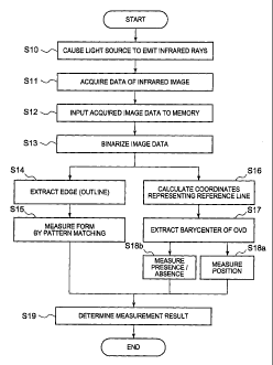
An OVD inspection method and apparatus according to
Example 2 of the present invention are applied to online
inspection on the production line.
CA 02578857 2007-03-02
29
The apparatus for executing online inspection to check
the quality including the OVD attachment state of a printed
product during conveyance has, as main elements, a linear light
source 8, an image input means 12 including a CCD line sensor
camera 7 (to be referred to as a CCD line sensor camera
hereinafter) with a visible light cutting infrared transmitting
filter and an input unit 20, and an image processing means 13,
as shown in Fig. 16. An inspection cylinder 9 conveys a printed
product 3 as an inspection target with an OVD.
The inspection cylinder 9 can use a known conveyance
scheme with, e.g., grippers or a suction system. In Example 2,
grippers grip an end of a printing paper sheet, and the rear part
of the sheet with respect to the conveyance direction is fixed by
a suction system. If the inspection cylinder 9 is not used, a
sheet conveyance scheme with a belt conveyor or chain grippers
can be used to inspect the printed product 3 as the inspection
target with the OVD online during conveyance on the production
line. In this case, fluttering of the sheet is preferably
minimized.
As shown in the flowchart of Fig. 17, the printed product
3 with the OVD, which is conveyed by the inspection cylinder 9,
is irradiated with light containing infrared rays from the linear
light source 8 (S21). At this time, the irradiation angle is set
to 30 with respect to the lens of the CCD line sensor camera 7
due to the same reason as in Example 1.
The CCD line sensor camera 7 repeatedly captures, for
each line, an image of light in the infrared range reflected by
the printed product 3 irradiated with the light containing
infrared rays, thereby acquiring one-dimensional data of an
infrared image (S22).
The image input means 12 sequentially inputs, in time
series, the one-dimensional image data of the region including
the OVD acquired by the CCD line sensor camera 7, thereby
generating two-dimensional image data (S23). The CCD line
sensor camera used here has a high spectral sensitivity in the
infrared range, as in Example 1. The effective sensitivity falls
CA 02578857 2007-03-02
within the wave range from 400 [nm] to 1,000 [nm], and the
peak spectral sensitivity falls within the wave range from 700
[nm] to 800 [nm], as shown in Fig. 6. The CCD line sensor
camera 7 having the above-described characteristic acquires the
5 image data of the region including the OVD. The acquired
image data is a monochrome image, as in Example 1.
The acquired image data is input to the memory (S25).
The image processing means 13 binarizes the image data (S26).
Extracting the edge (outline) of the OVD from the processed
10 binary data (S27) facilitates the subsequent process.
The operation unit in the image processing means 13
compares the binarized image data with reference image data
stored in advance by pattern matching (S28). The reference
image data contains reference image data with a standard OVD
15 and the reference data of a reference position, as in Example 1.
In this process, the binary data of each of the reference image
data, the reference image data, and the image data of the
inspection target is segmented into n x m pixels (n and m are
integers; n >_ 1, and m >_ 1). Then, the image data are
20 compared with each other. The form is compared and
inspected by pattern matching. Determination is done for each
target pixel. When the matching rate is 90% or more, the OVD
is determined as an acceptable product. The matching rate and
the area per pixel can be set to desired values.
25 After the binarization process in step S26, position
measurement for attachment position inspection is executed in
parallel to form inspection by using a reference mark 14 which
is printed in advance by an infrared absorbing ink on the printed
product 3 near the attachment position of the OVD 4 as a
30 reference position.
For position measurement, a barycenter t of the
reference mark 14 is calculated (S29). Next, the OVD 4 is
specified from the image data, and a barycenter 0 is calculated
in a similar way. On the basis of the barycenter t (X0,Y0) of
the reference mark 14 obtained by the calculation, the
barycenter 0 (X1,Y1) of the OVD image is calculated and
CA 02578857 2007-03-02
31
extracted (S30). X1-XO and Y1-YO are calculated from the
coordinate values of the barycenter t (XO,YO) of the reference
mark 14 and the barycenter 0 (X1,Y1) of the OVD 4. Position
measurement is done on the basis of the numerical values
(S31a). The presence/absence of an OVD is determined by
executing barycenter extraction from the image data that has
extracted the OVD 4, and calculating the area of the target OVD
(S31b). In this way, the position and attachment state quality
of the OVD are inspected, as in Example 1.
If it is difficult to print the reference mark on the base
material by using an infrared absorbing ink, a position
representing the base material, e.g., a corner of the base
material may be used as the reference position. In this case, it
is possible to manage the quality of attachment position by
calculating X1-XO and Y1-YO in accordance with the same
procedure as described above and comparing them with the
reference data.
The attachment state quality inspection including form
inspection and position inspection is executed by pattern
matching. The image processing means 13 determines the
quality on the basis of the inspection results (S32). If it is
determined on the basis of the determination results that the
form is not acceptable, a determination lamp indicates it, or the
printed product is discarded. A known means can be used as
the display or discarding means. With the above-described
procedure, OVD inspection can be done by almost the same
method both online and offline.
Fig. 18 shows a state wherein the printed product 3 with
the OVD 4, which is conveyed by the inspection cylinder 9 in
online inspection, is slightly floating from the inspection cylinder
9 or fluttering. Especially when the printed product 3 by
photocomposing with a plurality of OVDs 4 as shown in Fig. 19
is conveyed at a high speed, the base material may flutter or
undulate during conveyance. Even in this case, according to
Examples 1 and 2, the attachment portion of the OVD 4 is
extracted by infrared rays. Hence, it is possible to always
CA 02578857 2007-03-02
32
capture and input stable image data even under these
circumstances.
For example, when an OVD is attached to the base
material, and a print pattern of an infrared absorbing ink or a
pair of print patterns of an infrared absorbing ink and an
infrared transmitting ink are formed in a region different from
the OVD, the print patterns can be inspected by using the OVD
inspection method and apparatus of Example 1 or 2.
It is necessary to register the reference image data of
the OVD and/or the data of the print pattern of the infrared
absorbing ink in advance. The OVD and print pattern cab be
inspected simultaneously by registering the reference image
data in advance. Print pattern inspection can be done to check
its position, area, and form, like OVD inspection.