Note: Descriptions are shown in the official language in which they were submitted.
CA 02587051 2007-04-24
WO 2006/050052 PCT/US2005/038849
ORGANIC-COMPLEX THIN FILM FOR NONVOLATILE
MEMORY APPLICATIONS
CROSS-REFERENCE OF RELATED APPLICATION
This application claims priority to U.S. Provisional Application No.
60/623,721
filed October 28, 2004, the entire contents of which are hereby incorporated
by reference.
BACKGROUND
1. Field of Invention
The present invention relates to an organic composite material having
bistability
of an electrical property, electronic or electro-optic devices having the
organic composite
material and methods of use.
2. Discussion of Related Art
In recent years, organic electronic devices have been replacing inorganic-
dominated electronic and opto-electronic devices, such as light emitting
diodes C.W.
Tang and S.A. VanSlyke, Appi. Phys. Lett. 51, 913, (1987), R.H. Friend, R.W.
Gymer, A.B. Holmes, J.H. Burroughes, R.N. Marks, C. Taliani, D.D.C. Bradley,
D.A.
Dos Santos, J.L. Bredas, M. Logdlund, and W.R. Salaneck, Nature 397, 121
(1999),
solar cells N.S. Sariciftci, L. Smilowitz, A.J. Heeger and F. Wudl, Science
258, 1474
(1992), and transistors D.J. Gundlach, Y.Y. Lin, T.N. Jackson, S.F. Nelson,
and D.G.
Schlom, IEEE Electron Device Lett. 18, 87 (1997), due to the extraordinary
advantages of organic materials. One of the primary appeals of organic
materials is
fabricating low-cost electronic devices via simple solution processes, thermal
evaporation, inkjet printing, stamping, etc. M. Baldo, M. Deutsch, P. Burrows,
H.
Gossenberger, M. Gerstenberg, V. Ban, and S. Forrest, Adv. Mat. 10, 1505,
(1998);
and F. Gamier, R. Hajlaoui, A. Yassar, and P. Srivastava, Science 265, 1684
(1994).
Other attributes of organic materials, particularly polymeric materials,
include
compatibility with flexible substrates, mechanical durability, and diversity
of the
-1-
CA 02587051 2007-04-24
WO 2006/050052 PCT/US2005/038849
chemical structure. Electrical bistable phenomena in organic thin films has
been a
subject of interest for quite some years now. H. Carchano, R. Lacoste, and Y.
Segui,
Appl. Phys. Lett. 19, 414, (1971); R. S. Potember, T. O. Poehler, and D. O.
Cowman,
Appl. Phys. Lett. 34, 405, (1979); L. P. Ma, J. Liu, and Y. Yang, Appl. Phys.
Lett. 80,
2997 (2002) incorporated by reference herein; L. P. Ma, S. M. Pyo, J. Y.
Ouyang, Q.
F. Xu, and Y. Yang, Appl. Phys. Lett. 82, 1419, (2003) incorporated by
reference
herein; and A. Bandyopadhyay, and A. J. Pal, Appl. Phys. Lett. 84, 999,
(2004).
There remains a need for thin film memory elements that can be used to replace
the
sophisticated inorganic memory devices. Organic electron donor and acceptor
materials have been used for preparing organic composite thin films. Charge
transfer
may occur between molecules after applying a voltage pulse and electrical
bistability
is observed in the composite film. W. Xu, G.R. Chen, R.J. Li, and Z.Y. Hua,
Appl.
Phys. Lett. 67, 2241, (1995); and L.P. Ma, W.J. Yang, Z.Q. Xue, and S.J. Pang,
Appl.
Phys. Lett. 73, 850, (1998), incorporated by reference herein. However, most
of the
organic thin films are fabricated by thermal evaporation in high vacuum and
the
requirements for the evaporation conditions are very strict. Hence, there is a
need to
develop a process with easily controlled parameters.
SUMMARY
Further objectives and advantages will become apparent from a consideration
of the description, drawings, and examples.
An electronic or electro-optic device according to an embodiment of this
invention has a first electrode, a second electrode spaced apart from the
first electrode,
and an organic composite layer disposed between the first electrode and the
second
electrode. The organic composite layer is composed of an electron donor
material, an
electron acceptor material, and a polymer matrix material. The organic
composite
layer exhibits substantial bistability of an electrical property.
An organic-composite material for an electronic or electro-optic device is
composed of an electron acceptor material, an electron donor material, and a
polymer
-2-
CA 02587051 2007-04-24
WO 2006/050052 PCT/US2005/038849
matrix material. The organic-composite material exhibits substantial
bistability in an
electrical property.
A method of storing and retrieving information includes applying a first
voltage between first and second electrical leads having a layer of an organic
composite material disposed therebetween. The first voltage causes a change in
an
electrical property state in at least a portion of the layer of organic
composite material.
The method also includes applying a second voltage to the first and second
electrical
leads and measuring an electrical current between the first and said second
electrical
leads, and determining an information storage state based on the measured
electrical
current.
BRIEF DESCRIPTION OF THE DRAWINGS
The invention is better understood by reading the following detailed
description with reference to the accompanying figures in which:
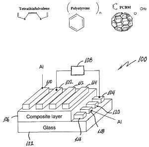
Figure 1 is a schematic illustration of an organic memory device according to
an embodiment of the current invention. Chemical structures of organic
materials that
can be used are also shown.
Figure 2 shows an atomic force microscope (AFM) micrograph image showing
surface topography of the organic composite film.
Figure 3 shows I-V curves of a device according to an embodiment of the
current invention having structure Al./PS:PCBM:TTF/Al. (a), (b) and (c)
represent the
first, second, and third bias scans, respectively. The arrow in the figure
indicates the
voltage-scanning direction.
Figure 4 shows write-read-erase cycles for the device
Al/(Polystyrene:TTF:PCBM)/Al according to an embodiment of this invention. The
top and bottom curves are the applied voltage and the corresponding current
response,
respectively. "1" and "0" in the bottom figure indicate the device in the high
and low
conductivity states, respectively.
-3-
CA 02587051 2007-04-24
WO 2006/050052 PCT/US2005/038849
Figure 5 shows retention characteristics of the organic memory device of
Figure 3 in ON and OFF states under a constant bias (0.5V) in vacuum.
Figure 6 shows typical frequency dependence of capacitance of the device of
Figure 3 in both ON-state and OFF-state.
Figure 7 shows the analysis of I-V characteristics for the device of Figure 3
at
(a) the high conductivity state (b) the low conductivity state.
Figure 8 shows UV-Vis spectra of (a) TTF (b) PCBM (c) PCBM and TTF in
1,2-dichlorobenzenic.
DETAILED DESCRIPTION
In describing embodiments of the present invention illustrated in the
drawings,
specific terminology is employed for the sake of clarity. However, the
invention is
not intended to be limited to the specific terminology so selected. It is to
be
understood that each specific element includes all technical equivalents which
operate
in a similar manner to accomplish a similar purpose.
According to an embodiment of this invention, electrical bistability in a two-
terminal structure is provided with an organic-composite thin film sandwiched
between metal electrodes. The thin film, may include polystyrene as the
matrix,
methanofullerene [6,6]-Phenyl C61-Butyric acid Methyl ester (PCBM) as an
organic
electron acceptor and tetrathiafulvalene (TTF) as an organic electron donor
that can be
formed by solution process. The polystyrene can be replaced by other polymers,
such
as poly(methyl methacrylate), poly(vinyl acetate), poly(ethyl methacrylate),
poly(4-
vinylpyridine), polyvinylpyrrolidone, poly(allylamine), poly(acrylamide),
poly(9-
vinylcarbazole), polyacenaphthylene, poly[2-methoxy, 5-(2'-ethyl-hexyloxy)-p-
phenylene-vinylene], polyfluorene, polyaniline and polythiophene. In addition,
TTF
can be replaced by other electron donors, such as tetraselenafulvalene,
hesamethyltetrathiafulvalene, hexamethyltetraselenafulvalene,
4,4',5,5',6,6',7,7'-
octahydrodibenzotetrafulvalene, 2,5-bis(1,3-dithiol-2-ylidene)-1,3,4,6-
tetrathiapentalene, bis(ethylenedithio)tetrathaifulvalene,
bis(methylenedithio)tetrathiafulvalene, tetramethyltetrathiafulvalene,
-4-
CA 02587051 2007-04-24
WO 2006/050052 PCT/US2005/038849
tetramethyltetraselenafulvalene, dimethyl(ethylenedithio)-
diselenadithiafulvalene,
methylenedithiotetrathiafulvalne, tetrathioanthracene, 2,3-
dimethyltetrathioanthracence, tetrawselenoanthracence, 2,3-
dimethyltetraselenoanthracene, copper phthalocyanine (CuPc), zinc (II)
phthalocyanine (ZnPc), ferrocence and copper (II) 2,9,16,23-tetra-tert-butyl-
29H,
31 H-phthalocyanine, and PCBM also can be replaced by other electron
acceptors,
such as tetracyanoquinodimethane, tetracyanoethylene, 1,2,3,4,5,6-
tetrafluobenzen, p-
chloranil, 2,5-dimethyl-N,N-dicyanoquinone diimine,
dichlorodicyanobenzoquinone,
tetracyanonaphthquinodimethane, 8- hydroquinone, fullerenes (including C60,
C70,
C76, C78, C84), fullerenols, N-ethyl-polyamino-fullerene, N-methyl-
fulleropyrrolidine, and methanofullerene [61]-carboxylic acid. However,
general
concepts of this invention are not limited to only the above-noted materials.
The
device according to an embodiment of the invention exhibits repeatable
electrical
transition between two states with a difference in conductivity of three
orders of
magnitude. The device according to this embodiment of the invention shows fast
switching response between the two states and nonvolatile behavior at either
state for
several weeks. The two states of this device can be precisely controlled by
applying
an appropriate voltage pulse several times without any significant device
degradation.
Therefore, this device can be used as a low-cost, high density, nonvolatile
organic
memory element, particularly when stacked multilayer memory cells are formed.
The
switching mechanism is attributed to the electric-field induced charge
transfer
between PCBM and TTF in the composite film.
In accordance with an embodiment of the present invention, we provide an
electric field induced current-controlled memory device using an organic
composite
thin film that is composed of an electron donor and an acceptor in a polymer
matrix.
The electrical bistability effect occurs in a two-terminal structure with an
organic
composite film, prepared by an easy solution process, sandwiched between two
metal
electrodes.
Figure 1 is a schematic illustration of an electronic device 100 according to
an
embodiment of this invention. A first electrode 102 and a second electrode 104
are
-5-
CA 02587051 2007-04-24
WO 2006/050052 PCT/US2005/038849
spaced apart with an organic-composite material 106 disposed therebetween. The
organic-composite material may be a thin film layer in some embodiments of
this
invention. The electrodes 102, 104 may be selected from any suitable
electrically
conductive material for the particular application. The examples discussed in
this
specification include aluminum electrodes. However, the electrodes are not
limited to
just aluminum. The composite layer 106 comprises an electron donor material,
an
electron acceptor material, and a polymer matrix material. The organic
composite
layer 106 exhibits bistability in an electrical property. A voltage applied
between
electrodes 102 and 104 by an input voltage source 108 can cause a change in an
electrical property of the organic-composite layer 106, depending on the
applied
voltage. An applied electric field will be most intense in the region where
the
electrodes 102 and 104 come closest together. Consequently, when one applies a
voltage to electrodes 102 and 104 it can cause a change in an electrical
property of the
organic-composite material 106 proximate a region of smallest distance between
the
electrodes 102 and 104 while not changing the electrical property away from
that
proximate region.
The electronic device 100 according to this embodiment of the invention may
also include a plurality of electrodes 110, 112 and 114 that are substantially
parallel
with the first electrode 102 and arranged substantially in a first layer of a
plurality of
electrodes. Similarly, a plurality of electrodes 116, 118 and 120 may be
provided and
arranged substantially parallel to the second electrode 104 to form a second
layer of a
plurality of electrodes. Although Fig. 1 illustrates four electrodes in each
of the first
and second layers of electrodes, the invention is not limited to any
particular number.
Furthermore, a device may include stacks of structures such as the electronic
device
100. The first layer of a plurality of electrodes 110, 112, 114 and 102 and
the second
layer of a plurality of electrodes 116, 118, 120 and 104 provide a plurality
of regions
that are addressable at regions around where two electrodes come closest
together.
The plurality of electrodes 116, 118, 120 and 104 may be deposited on a
substrate
122. The layer of organic-composite material 106 may be deposited on the
substrate
122 and the first plurality of electrodes 116, 118, 120 and 104. The substrate
122 may
-6-
CA 02587051 2007-04-24
WO 2006/050052 PCT/US2005/038849
be selected from materials according to the desired application. One may
select the
substrate to be an electrically nonconductive material, or combinations of
electrically
nonconductive materials. For example, it may be selected to be a glass
substrate.
Example
Examples of chemical structures of the materials of the device of the
embodiment of Fig. l are indicated in Fig. 1. The device fabrication procedure
involves deposition of aluminum (Al) 0.2 mm in width and 75nm in thickness on
thoroughly cleaned glass substrates to form the bottom electrode by thermal
evaporation under vacuum (below 6 x 10⁻⁶ Torr) in this example. Before spin-
coating
the composite layer, the substrates were exposed to UV-ozone treatment for 15
min.
Then, the polymer film was formed by spin-coating 1,2-dichlorobenzenic
solution of
1.2 wt. % polystyrene and 0.8 wt. % TTF and 0.8 wt. % PCBM. Good results have
been obtained by using amounts of electron acceptor (PCBM) and electron donor
(TTF) to be about the same. However, the relative amounts may vary. In
addition
good results were obtained using weight ratios of polymer matrix (PS):electron
acceptor (PCBM):electron donor (TTF) in a range of about 1:1:1 to 10:1:1.
The deposited film was thermally annealed at 80 C for 30 min. The thickness
of the organic film was about 50nm. The surface of the organic film was
investigated
by atomic force microscopy (AFM) and the surface scans are shown in Fig. 2.
The
figure shows a uniform surface with 5A root-mean-square roughness. Finally, 75
nm
of Al was deposited as the top electrode resulting in the Al/Organic composite
layer/Al sandwich structure of the memory cells according to an embodiment of
the
invention. The thicknesses of the organic layer and the metal electrodes were
calibrated with Dektak 3030 thickness profilometer. The active device area,
which is
defined as the cross-section of the bottom and top electrode, was 0.2x0.2 mm
2. The
current-voltage (I-V) characteristics of the 'devices were measured with a
Hewlett
Packard 4155B semiconductor analyzer. The capacitance measurements were
carried
out with a HP 4284A Precision LCR Meter. The write-read-erase cycles were
measured by a programmable Keithley 2400 source meter and recorded with a four-
-7-
CA 02587051 2007-04-24
WO 2006/050052 PCT/US2005/038849
channel oscilloscope (Tektronix TDS 460A). All the electrical measurements
were
performed in a vacuum lower than 1 x 10⁻⁴ Torr at the room temperature.
Typical I-V characteristics of bistable devices according to this embodiment
of
the invention are shown in Fig.3. The devices exhibit two states of different
electrical
conductivity at the same voltage. During the first bias scan (curve (a)), low
current
was observed for the devices in bias range from OV to 2.6V. A sharp increase
in the
cunent, from 10-7 A to 104 A, took place at around 2.6V indicating the
transition of the
devices from a low conductivity state (OFF state) to a high conductivity state
(ON
state). After the transition, the devices remained in that state even after
the bias was
removed, as shown in the subsequent voltage scan (curve (b)). The ratio of the
difference in conductivity between two states was more than three orders of
magnitude. The low conductivity state can be recovered by simply applying
either a
large positive voltage pulse or a negative voltage pulse. Fig.3 (curve(c))
shows that
the current suddenly dropped from 104 A to 10-6A at -6.5V. In addition, the
devices in
the low conductivity state could be turned to the high conductivity state by a
pulse of
5V with a width smaller than 100 ns. Also, the high conductivity state could
be
turned to a low conductivity state by a pulse of -9V with a width smaller than
100 ns.
The electrical switching between low and high conductivity states was
performed numerous times. A voltage pulse of 5V can induce the device to the
high
conductivity "1" state. This "1" state can be read by a pulse of 1 V with a
current of
_10-5A. A negative bias of -9V can erase this "1" state to the low
conductivity "0"
state. The "0" state can be detected by a pulse of 1 V with a current of -
10"8A. The
electrical bistability of this device can be precisely coiitrolled by applying
an
appropriate voltage pulse numerous times without any significant device
degradation.
The precisely controlled write-read-erase cycles were conducted on our memory
devices with good rewritable characteristics as shown in Fig. 4. Moreover,
once the
device switches to either state it remains in that state for a prolonged
period of time.
The stability of the devices under stress was measured in the continuous bias
condition. A constant voltage (0.5V) was applied to the device in the Off and
On state
and the current recorded at different times. As can be seen from Fig. 5(a),
there is no
-8-
CA 02587051 2007-04-24
WO 2006/050052 PCT/US2005/038849
significant degradation of the devices in both Off and On states even after 12
hours of
continuous stress test. In addition, the retention ability was tested by
leaving several
devices in the high conductivity state without applying bias under a nitrogen
environment. Fig. 5(b) shows that once we wrote an ON-state, the devices
remained
in that state for several days to weeks. These write-read-erase cycles and the
duration
test demonstrated that such a device could be used as a nonvolatile memory
device.
Electrical transitions have been observed previously in some polymer films,
and the mechanism was attributed to the formation of conductive filaments
between
two metal electrodes under a high electric field. R. S. Potember, T. O.
Poehler, and D.
O. Cowman, Appl. Phys. Lett. 34, 405, (1979) ; and H.K. Henish, and W.R.
Smith,
Appl. Phys. Lett. 24, 589, (1974). Alternating-current impedance studies, from
20 to
106 Hz, indicate that the electronic transitions in our device are different
from
dielectric breakdown found in polymer films. We observed the capacitance was
lowered by about an order of magnitude for the device with polystyrene film
after the
breakdown. However, we have observed the frequency dependence of the
capacitance
of our device in the ON-state and the OFF-state, as shown in Fig. 6. In the
frequency
range of 104-106 Hz the capacitance remained almost constant in both states.
This
suggests that the capacitance is not affected by the space charge, but
determined by
the dielectric constant of the bulk material between the two electrodes. In
the low-
frequency region (below 104 Hz) the capacitance in the ON-state increased
dramatically with decreasing frequency, whereas, there was little increase in
the OFF-
state. Polystyrene acts as an inert matrix for TTF and PCBM, and does not play
a role
in the electronic transition. The capacitance difference between the two
states
indicates that the charge carriers are generated within the composite film
under an
electrical field. However, there is a possibility that when PS is replaced by
a
conjugated polymer (such as poly(2-methoxy-5-(ethylhexyloxy)-1,4-
phenylenevinylene) or polyfluorene ) other phenomena might be observed, for
example, a light emitting memory cell (in two terminal device), or a permanent
on
transistor (in three terminal device).
-9-
CA 02587051 2007-04-24
WO 2006/050052 PCT/US2005/038849
The device according to this embodiment of the invention exhibits a nonlinear
relationship between current and applied electric field before and after the
electrical
transition. The conduction mechanism for Al/ (PS:PCBM:TTF)/Al in the low
conductivity state may be due to the presence of a small amount of impurity or
hot
electron injection. The Log (I) vs. V1/Z plot in the voltage range from 0 to
1.7V before
the electrical transition shows linearity, as shown in Fig. 7(a). Such
linearity suggests
that the conduction process can be explained by Schottky emission behavior. A
linear
relation was observed for Log (I/V) vs. V1/Z plot for the device after
electrical
transition. The Poole-Frenkel conduction mechanism is probable for the device
in the
high conductivity state, as shown in Fig. 7(b). This Poole-Frenkel emission
was
further confirmed by using electrodes of dissimilar work functions, i.e. with
the
ITO/(PS: PCBM:TTF)/Al configuration, and symmetric I-V characteristic for both
the
polarities were observed. Hence, an electrical transition from the Schottky
mechanism to Poole-Frenkel is induced for the device under a high electrical
field.
'15 The electrical transition presumably can be attributed to an electrical-
field
induced charge transfer between TTF and PCBM in the film. It has already been
demonstrated that TTF and PCBM can be electron donor and acceptor,
respectively.
M.R. Bryce, Adv. Mat. 11, 11, (1999); N. Marty'n; L. Sa'nchez, M.A. Herranz,
and
D.M. Guldi, J. Phys. Chem. A 104, 4648, (2000). The UV-Vis spectra didn't show
significant change when we blended TTF and PCBM, as shown in Fig. 8.
Therefore,
prior to the electronic transition there is no interaction between TTF and
PCBM.
Concentration of charge carriers due to impurity in the film is quite low, so
that the
film has low conductivity. However, when the electrical field increases to a
certain
value, electrons in the HOMO of TTF may gain enough energy to transfer to
PCBM.
Consequently, the highest occupied molecular orbit (HOMO) of TTF becomes
partially filled, and TTF and PCBM are charged positively and negatively,
respectively. Therefore, carriers are generated and the device exhibits sharp
increase
in conductivity after the charge transfer.
In conclusion, electrical bistable devices utilizing organic materials with
simplified structure have been provided by easy fabrication methods using spin
-10-
CA 02587051 2007-04-24
WO 2006/050052 PCT/US2005/038849
coating and thermal evaporation. The control of voltage values permit devices
to be
designed with the required characteristics. In addition, the devices exhibit
repeatable
and nonvolatile electrical bistable properties. Furthermore, the devices have
the
potential to be stacked with several memory layers on top of each other, thus
drastically increasing the density compared to nonvolatile memories based on
inorganic materials. Finally, when a conjugated polymer is used to replace PS,
we
expect novel phenomena such as bistable LEDs and permanent-on transistors.
The embodiments illustrated and discussed in this specification are intended
only to teach those skilled in the art the best way known to the inventors to
make and
use the invention. Nothing in this specification should be considered as
limiting the
scope of the present invention. The above-described embodiments of the
invention
may be modified or varied, and elements added or omitted, without departing
from the
invention, as appreciated by those skilled in the art in light of the above
teachings. It
is therefore to be understood that, within the scope of the claims and their
equivalents,
the invention may be practiced otherwise than as specifically described.
-11-