Note: Descriptions are shown in the official language in which they were submitted.
CA 02590684 2007-06-14
WO 2006/065937 PCT/US2005/045316
AQUEOUS CARBON NANOTUBE APPLICATOR LIQUIDS AND METHODS
FOR PRODUCING APPLICATOR LIQUIDS THEREOF
Cross-Reference to Related Applications
[0001] This application claims the benefit under 35 U.S.C. 119(e) of U.S.
Provisional
Patent Application Nos. 60/636673, filed December 16, 2004, and 60/704858,
filed August
2, 2005, both of which are assigned to the assignee of this application, and
both of which
are incorporated herein by reference in their entirety.
[0002] This application is related to the following applications, all of which
are
assigned to the assignee of this application, and all of which are
incorporated by reference
in their entirety: Nanotube Films and Articles (U.S. Patent No. 6706402) filed
April
23, 2002;
Methods of Nanotube Films and Articles (U.S. Patent No. 6835591) filed April
23, 2002; and
Patterning of Nanoscopic Articles (U.S. Patent Appl. No. 10/936119) filed on
September 8, 2004.
Background
Technical Field
[0003] This invention describes applicator liquids for use in the preparation
of
nanotube films. Such applicator liquids are used in creating films and fabrics
of nanotubes
or mixtures of nanotubes and other materials on a variety of substrates
including silicon,
plastics, paper and other materials. In particular, the invention describes
applicator liquids
containing nanotubes for use in electronics fabrication processes.
Furthermore, the
applicator liquids meet or exceed specifications for a semiconductor
fabrication facility,
including a class 1 environment.
CA 02590684 2007-06-14
WO 2006/065937 PCT/US2005/045316
Discussion of Related Art
[0004] Nanotubes are useful for many applications; due to their electrical
properties
nanotubes may be used as conducting and semi-conducting elements in numerous
electronic elements. Single walled carbon nanotubes (SWNTs) have emerged in
the last
decade as advanced materials exhibiting interesting electrical, mechanical and
optical
properties. However, the inclusion or incorporation of the SWNT as part of
standard
microelectronic fabrication process has faced challenges due to a lack of a
readily available
application method compatible with existing semiconductor equipment and tools
and
meeting the stringent materials standards required in the electronic
fabrication process.
Standards for such a method include, but are not limited to, non-toxicity, non-
flammability,
ready availability in CMOS or electronics grades, substantially free from
suspended
particles (including but not limited to submicro- and nano-scale particles and
aggregates),
and compatible with spin coating tracks and other tools currently used by the
semiconductor industry.
[0005] Individual nanotubes may be used as conducting elements, e.g. as a
channel in a
transistor, however the placement of millions of catalyst particles and the
growth of
millions of properly aligned nanotubes of specific length presents serious
challenges.
United States Patent Nos. 6,643,165 and 6,574,130 describe electromechanical
switches
using flexible nanotube-based fabrics (nanofabrics) derived from solution-
phase coatings
of nanotubes in which the nanotubes first are grown, then brought into
solution, and applied
to substrates at ambient temperatures. Nanotubes may be derivatized in order
to facilitate
bringing the tubes into solution, however in uses where pristine nanotubes are
necessary, it
is often difficult to remove the derivatizing agent. Even when removal of the
derivatizing
agent is not difficult, such removal is an added, time-consuming step.
[0006] Generally, until now the solvents used to disperse the carbon nanotubes
are
organic solvents such as orthodichlorobenzene (ODCB) and chloroform. The
solutions are
stable but the solvents have the disadvantage of not solubilizing clean carbon
nanotubes
which are free of amorphous carbon. We have developed a method to remove most
of the
2
CA 02590684 2007-06-14
WO 2006/065937 PCT/US2005/045316
amorphous carbon and solubilize the carbon nanotubes at high concentrations in
water via
pH manipulation.
[0007] There have been few attempts to disperse SWNTs in aqueous and non-
aqueous
solvents. Chen et al. first reported solubilization of shortened, end-
functionalized SWNTs
in solvents such as chloroform, dichloromethane, orthodichlorobenzene (ODCB),
CS2,
dimethyl formamide (DMF) and tetrahydrofuran (THF). See, "Solution Properties
of
Single-Walled Nanotubes," Science 1998, 282, 95-98. Ausman et al. reported the
use of
SWNTs solutions using sonication. The solvents used were N-methylpyrrolidone
(NMP),
DMF, hexamethylphosphoramide, cyclopentanone, tetramethylene sulfoxide and
8-caprolactone (listed in decreasing order of carbon nanotube solvation).
Ausman at el.
generally conclude that solvents with good Lewis basicity (i.e., availability
of a free
electron pair without hydrogen donors) are good solvents for SWNTs. See,
"Organic
Solvent Dispersions of Single-Walled Carbon Nanotubes: Toward Solutions of
Pristine
Nanotubes," J. Phys. Chem. B 2000, 104, 8911. Other early approaches involved
the
fluorination or sidewall covalent derivatization of SWNTs with aliphatic and
aromatic
moieties to improve nanotube solubility. See, e.g., E. T. Mickelson et al.,
"Solvation of
Fluorinated Single-Wall Carbon Nanotubes in Alcohol Solvents," J. Phys. Chem.
B 1999,
103, 4318-4322.
[0008] Full-length soluble SWNTs can be prepared by ionic functionalization of
the
SWNT ends dissolved in THF and DMF. See, Chen et al., "Dissolution of Full-
Length
Single-Walled Carbon Nanotubes," J. Phys. Chem. B 2001, 105, 2525-2528 and J.
L. Bahr
et al Chem. Comm. 2001, 193-194. Chen et al. used HiPCOTM as-prepared (AP)-
SWNTs
and studied a wide range of solvents. (HiPCOTM is a trademark of Rice
University for
SWNTs prepared under high pressure carbon monoxide decomposition). The
solutions
were made using sonication.
[0009] Bahr et al. ("Dissolution Of Small Diameter Single-Wall Carbon
Nanotubes In
Organic Solvents," Chem. Comm., 2001, 193-194) reported the most favorable
solvation
results using ODCB, followed by chloroform, methylnaphthalene,
bromomethylnaphthalene, NMP and DMF as solvents. Subsequent work has shown
that
3
CA 02590684 2007-06-14
WO 2006/065937 PCT/US2005/045316
good solubility of AP-SWNT in ODCB is due to sonication induced polymerization
of
ODCB, which then wraps around SWNTs, essentially producing soluble polymer
wrapped
(PW)-SWNTs. See Niyogi et al., "Ultrasonic Dispersions of Single-Walled Carbon
Nanotubes," J. Phys. Chem. B 2003, 107, 8799-8804. Polymer wrapping usually
affects
sheet resistance of the SWNT network and may not be appropriate for electronic
applications where low sheet resistance is desired. See, e.g., A. Star et al.,
"Preparation and
Properties of Polymer-Wrapped Single-Walled Carbon Nanotubes," Angew. Chem.
Int.
Ed. 2001, 40, 1721-1725 and M. J. O'Connell et al., "Reversible Water-
Solubilization Of
Single-Walled Carbon Nanotubes By Polymer Wrapping," Chem. Phys. Lett. 2001,
342,
265-271.
[0010] While these approaches were successful in solubilizing the SWNTs in a
variety
of organic solvents to practically relevant levels, all such attempts resulted
in the depletion
of the 7c electrons that are essential to retain interesting electrical and
optical properties of
nanotubes. Other earlier attempts involve the use of cationic, anionic or non-
ionic
surfactants to disperse the SWNT in aqueous and non aqueous systems. See,
Matarredona
et al., "Dispersion of Single-Walled Carbon Nanotubes in Aqueous Solutions of
the
Anionic Surfactant," J. Phys. Chem. B 2003, 107, 13357-13367. While this type
of
approach has helped to retain the electrical conductivity and optical
properties of the
SWNTs, most such methods leave halogens or alkali metals or polymeric
residues, which
tend to severely hamper any meaningful use in microelectronic fabrication
facilities.
Summary of the Invention
[0011] There is a need for a method of distributing nanotubes in a liquid
medium for
use in electronics applications. Such a method should allow for removal of
amorphous
carbon, leaving carbon nanotubes, a high concentration of CNTs in solution.
Such an
applicator liquid could be useful for making high-uniformity nanotube fabrics
on various
substrates including silicon. The use of such an applicator liquid would
require few
applications (i.e. spin coat applications), to produce a fabric of
controllable sheet resistance
4
CA 02590684 2007-06-14
WO 2006/065937 PCT/US2005/045316
with high uniformity. Such an applicator liquid could have many other
applications as
well.
[00I21 There remains a further need for methods that meet the criteria
outlined above
for low toxicity, purity, cleanliness, ease of handling and scalability.
[0013] One aspect of the invention is directed to an applicator liquid
containing
nanotubes and water useful in the preparation of nanotube fabrics and films.
According to
one aspect of the present invention, an applicator liquid for use in an
electronics fabrication
process includes an aqueous liquid medium containing a plurality of nanotubes
pretreated
to reduce the level of metal and particulate impurities to a preselected
level. The
concentration of the nanotubes in the liquid medium is at commercially
meaningful levels,
e.g., the nanotubes are at a concentration of greater than 1 mg/L. The
nanotubes are
homogeneously distributed in the liquid medium without substantial
precipitation or
flocculation.
[0014] In one or more embodiments of the invention, an applicator liquid for
preparation of a nanotube film or fabric includes a controlled concentration
of nanotubes
dispersed in water, wherein the controlled concentration is sufficient to form
a nanotube
fabric or film of preselected density and uniformity. The nanotubes are at a
concentration
of greater than 1 mg/L, or greater than 100 mg/L, or greater than 1000 mg/L.
The
nanotubes are homogeneously distributed in water without precipitation or
flocculation.
[0015] In one or more embodiments, an applicator liquid for preparation of a
nanotube
film includes a distribution of nanotubes in water, wherein the nanotubes
remain separate
from one another without precipitation or flocculation for a time sufficient
to apply the
applicator liquid to a surface.
[0016] In one aspect of the present invention, the applicator solution is
substantially
free of particulate and metallic impurities. The level of particulate and
metallic impurities
is commensurate with preselected fabrication requirements.
[0017] In another aspect of the invention, a nanotube composition is provided
including a plurality of nanotubes in water medium, wherein the nanotubes are
CA 02590684 2007-06-14
WO 2006/065937 PCT/US2005/045316
substantially separate from one another and homogeneously distributed
throughout the
water medium.
[0018] The fabrication processes can have varying requirements for solvent and
raw
material composition and purity. According to one aspect of the present
invention,
applicator solutions of varying composition and purity are provided for use in
these
fabrication processes having varying processing specifications and
environmental
requirements.
[0019] According to one aspect of the present invention, methods and
compositions for
creating nanotube applicator solutions for use in fabrication facilities
having high standards
of non-toxicity and purity are provided. Such processes include semiconductor
fabrication
processes, for example, CMOS and advanced logic and memory fabrications. Such
fabrication processes may produce devices having fine features, e.g., < 250
nm.
[0020] According to other aspects of the present invention, the nanotube
applicator
solutions are of a purity that is suitable for use in electronics fabrication
facilities having
less stringent standards for chemical composition and purity. Such processes
include, for
example, interconnect fabrication and fabrication of chemical and biological
sensors.
Brief Description of the Drawing
[0021] The invention is described with reference to the Drawing, which is
presented for
the purpose of illustration only and which is not intended to be limiting of
the invention.
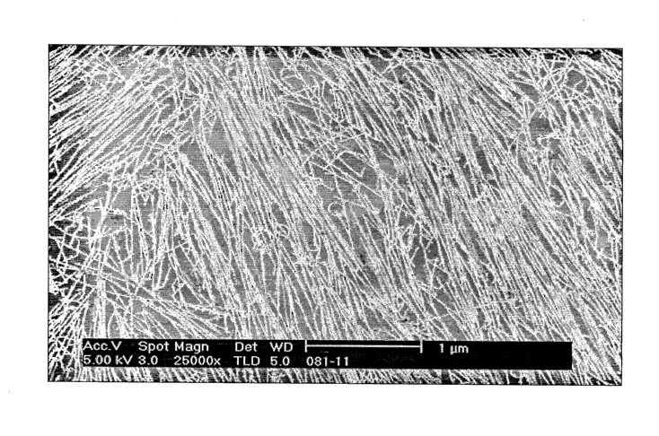
[0022] Figure 1 illustrates a typical scanning electron micrograph (SEM) of a
nanotube
fabric.
[0023] Figure 2 illustrates a typical micrograph of a purified nanotube
fabric.
[0024] Figure 3A illustrates a micrograph of a nanotube fabric created with
batch
centrifugation.
[0025] Figure 3B illustrates a micrograph of the nanotube fabric of Figure 3A
at higher
magnification.
[0026] Figure 4A illustrates a micrograph of a nanotube fabric created with
continuous
flow centrifugation.
6
CA 02590684 2007-06-14
WO 2006/065937 PCT/US2005/045316
[0027] Figure 4B illustrates a micrograph of the nanotube fabric of Figure 4A
at higher
magnification.
Detailed Description of the Invention
[0028] Nanotubes have been the focus of intense research efforts into the
development
of applications that take advantage of their electronic, biological, and/or
material
properties. In one or more embodiments, an applicator liquid containing
nanotubes is
prepared in water. The applicator liquid can be a spin-coatable liquid that
may be used to
create nanotube films and fabrics of substantially uniform porosity. Certain
embodiments
provide applicator liquids having a purity level that is commensurate with the
intended
application. Other applications provide applicator liquids meeting or
exceeding
specifications for class 1 semiconductor fabrication.
[0029] In one or more embodiments, an applicator liquid includes liquid medium
containing single-walled nanotubes, multi-walled nanotubes, or mixtures
thereof that is
stable enough for certain intended applications, such as spin coating in a
class 1 production
facility. The nanotubes in the applicator liquid remain suspended, dispersed,
solvated or
mixed in a liquid medium without substantial precipitation, flocculation or
any other
macroscopic interaction that would interfere with the ability to apply the
applicator liquid
to a substrate and form a uniform porosity. If there were significant
precipitation or
aggregation of the nanotubes, the nanotubes would clump together and form non-
uniform
films, which would be undesirable. The nature by which the nanotubes interact
with the
liquid medium to form a stable composition is not limited. Thus, for example,
the
nanotubes may be suspended or dispersed in the liquid medium or they may be
solvated or
solubilized in the liquid medium. The stable applicator liquid typically forms
a
homogeneous distribution of nanotubes in the liquid medium.
[0030] At the present time, it is desirable that the nanotubes remain
distributed in the
liquid medium without substantial precipitation, flocculation or other
macroscopic
interaction, for at least one hour, or for at least 24 hours, or even for at
least one week.
Substantial precipitation and flocculation and the like can be detected by a
variety of
methods. Precipitates and aggregates can be detected by visual inspection.
Alternatively,
7
CA 02590684 2007-06-14
WO 2006/065937 PCT/US2005/045316
precipitation or flocculation can be detected by analytical techniques, such
light scattering
or absorbance, or by observation of nanotubes once they are deposited on a
substrate from
the nanotube solution. A stable applicator liquid can exhibit prolonged
suspension
(typically several weeks to few months) of the SWNT in the medium with little
or no
detectable change in the scattered light intensity, or absorbance at a given
wavelength, or
viscosity.
[0031] Light scattering is measured using a monochromatic beam of light
traveling
through the solution. A change of light scattering intensity over time is
recorded usually by
a detector placed normal to the beam direction or from multiple detectors
placed at various
angles including the right angle. Another indicator especially at low
concentrations of
SWNT is the fall in absorbance (at a given wavelength) as a function of time.
Other
methods of determining the stability of a nanotube applicator liquid for its
intended purpose
will be apparent to those of skill in the art.
[0032] The nanotubes used in one or more embodiments of the present invention
may
be single walled nanotubes, multi-walled nanotubes, or mixtures thereof and
may be of
varying lengths. The nanotubes may be conductive, semiconductive or
combinations
thereof. Both conductive and semiconductive SWNTs are useful in the
manufacture of
nanotube films, articles and devices and can be used in the nanotube
applicator liquid
according to one or more embodiments of the invention. Thus, the applicator
liquid may be
integrated into current electronic fabrication processes including, by way of
example,
CMOS, bipolar-transistor, advanced memory and logic device, interconnect
device, and
chemical and biological sensor fabrications.
[0033] In selecting a liquid medium for the nanotube composition, the intended
application for the applicator liquid may be considered. For example, the
liquid medium of
the present inventionmay be an aqueous liquid medium that meets or exceeds
purity
specifications required in the fabrication of intended application. The
semiconductor
manufacturing industry demands adherence to the specific standards set within
the
semiconductor manufacturing industry for ultra-clean, static-safe, controlled
humidity
storage and processing environments. Many of the common nanotube handling and
8
CA 02590684 2007-06-14
WO 2006/065937 PCT/US2005/045316
processing procedures are simply incompatible with the industry standards.
Furthermore,
process engineers tend to resist trying unfamiliar technologies. According to
one aspect of
the present invention, a liquid medium for use in the applicator liquid is
selected based
upon its compatibility or compliance with the electronics and/or semiconductor
manufacturing industry standards.
[0034] In one aspect of the invention, applicator liquids include a plurality
of
single-walled nanotubes, multi-walled nanotubes, or mixtures thereof in water
as the liquid
medium. V~ater is readily available and accepted into all semiconductor
foundries. The
water used may be of high purity and may depend or be influenced by the end
use
application. For example, in CMOS applications the water may be high purity
having a
typical resistance of about 18 megaohms. Water can be readily purified,
creating a particle
free and contaminant free liquid. Water will generally not solvate
photoresists and is
compatible with current and advanced photoresists and lithographic processes.
[0035] Typical nanotube concentrations range from about 1 mg/L to 100 g/I,, or
from
about 1 mg/L to lg/L, or about 10 mg/L, or about 100 mg/L, or even about 1000
mg/L with
a common concentration used for memory and logic applications of 100 mg/L.
Such a
concentration is exemplary; various useful concentrations ranges depend upon
the
application. For example in the case where a monolayer fabric is desired, one
could use a
more diluted concentration with a single or a few applications of the
applicator liquid, e.g.,
by spin coating, to the substrate. In the event that a thick multilayer fabric
is desired, a
spraying technique could be employed with a nearly saturated composition of
nanotube in
the applicator liquid. The concentration is, of course, dependent upon the
specific liquid
medium choice, method of nanotube dispersion and type of nanotube used, e.g.,
single-walled or multiwalled.
[0036] Nanotubes may be prepared using methods that are well known in the art,
for
example, chemical vapor deposition (CVD) or other vapor phase growth
techniques
(electric-arc discharge, laser ablation, etc.). Nanotubes of varying purity
may also be
purchased from several vendors, such as Carbon Nanotubes, Inc., Carbolex,
Southwest
Nanotechnologies, EliCarb, Nanocyl, Nanolabs, and BuckyUSA (these and other
carbon
9
CA 02590684 2007-06-14
WO 2006/065937 PCT/US2005/045316
nanotube suppliers are known). Vapor-phase catalysts are typically used to
synthesize
nanotubes and, as a result, the nanotubes are contaminated with metallic
impurities.
Furthermore, formation of nanotubes may also be accompanied by the formation
of other
carbonaceous materials, which are also sources of impurities in the nanotubes.
[0037] In one or more embodiments of the present invention, metallic particles
and
amorphous carbon particles may be separated from nanotubes. The purification
process
may reduce alkali metal ions, halogen ions, oligomers or polymers as active or
inactive
chemical components as part of the SWNT solution. The applicator liquids
according to
certain embodiments of the present invention may be substantially free of high
levels of
these particulate and/or insoluble materials (as well as other soluble
materials that are
incompatible with the semiconducting fabrication process). The nanotube
solutions may
thus be purified for use in CMOS processing or other semiconducting
fabrication process.
[0038] Appropriate purification techniques may desirably remove impurities
without
affecting the nanotube chemical structure or electronic properties. Impurities
may be
removed for example, by dispersing the nanotubes in an acid solution to
dissolve metal
impurities, followed by separation of the nanotubes from the metallic
solution. For
example, an acid treatment with nitric acid or hydrochloric acid may be used.
The
purification technique may further treat the nanotubes with a base. For
example, after
treatment of the nanotubes with the acid, the nanotubes may further be treated
with a base
such as NH4OH (ammonia hydroxide), TMAH (tetramethylammonium hydroxide), or
other alkyl ammonium bases. The nanotubes may be treated with an acid and/or a
base in a
single or multiple steps. In some embodiments, nanotubes may be treated with a
concentrated acid and then a mild acid to obtain a dilute acid solution. In
some
embodiments, the nanotubes may be treated to substantially neutralize a dilute
acid
solution. For example, a dilute acid solution may be neutralized to have a pH
of about 6.5
to 7.5. Other suitable methods for metal removal include magnetic
purification.
[0039] Without being bound to theory, it may be possible that the acid
treatment serves
at least a dual function of dissolving the metal impurities and
functionalizing the carbon
nanotubes with carboxylic acid groups to render them soluble in water. In
addition, the
CA 02590684 2007-06-14
WO 2006/065937 PCT/US2005/045316
acid treatment may further aid in breaking down any amorphous graphitic carbon
impurities present in the raw CNT and functionalizing them with carboxylic
acid groups as
well. One or more additional acid treatment, possibly at weaker acidic
conditions than the
first acid treatment, may aid in removing metal impurities. The base treatment
may lead to
a solubility difference between the derivative CNTs and derivatized graphitic
carbon,
rendering the derivatized amorphous graphitic carbon nlore soluble in the
liquid medium.
Such solubility difference may facilitate separation of amorphous graphitic
carbon and
CNTs via subsequent filtration and/or centrifugation.
[0040] Amorphous carbon may be removed, for example, by one or a combination
of
high speed centrifugation. For example, non-limiting examples of high speed
centrifugation techniques may include ultracentrifugation, gravity filtration,
cross flow
filtration, vacuum filtration and others. Gravity filtration is a procedure
wherein the
dispersion can be filtered through a membrane under gravitational flow. Cross
flow
filtration is a procedure where a shearing force normal to the filtration
direction can be
applied by means of stirring or external, recirculative or non-recirculative
pumping.
Vacuum filtration is a procedure where the filtrate side of a membrane is
subjected to a
lower pressure to generate a differential pressure as a driving force for
filtration.
[0041] Alternatively, particulate may be removed from the applicator liquids
by using
continuous flow centrifuge at g forces between 60000-180000 and adequate flow
rates. The
usage of continuous flow centrifuge may lead to higher quality products,
reduced
manufacturing time, and can be less labor intensive. Continuous flow
centrifugation refers
to a method to separate or sediment particulate solids form a solution or
suspension using
centrifugal force applied with a continuous flow centrifuge. The continuous
flow
centrifuge may allow for particulate separation or removal from a solution in
a continuous
mode of operation of the centrifuge. Any commercially available 'high-g"
centrifuges or
ultracentrifuges may be utilized. The continuous flow centrifuge may have the
ability to
separate particles from solution by continuously feeding the solution to the
centrifuge rotor,
followed by particles separation or sedimentation, and continuous removal of
the
particulate free product from the centrifuge rotor. For example, lab scale
continuous flow
11
CA 02590684 2007-06-14
WO 2006/065937 PCT/US2005/045316
ultracentrifuges (that are capable of generating up to 10L of particulate free
product in one
hour) or manufacturing scale continuous flow centrifuges (that are capable of
generating to
100L particulate free product in one hour) may be utilized. A non-limiting
example of a lab
scale continuous flow ultracentrifuge may be the Sorvall Discovery 90/100 with
TCF32
rotor. A non-limiting example of a manufacturing scale continuous flow
ultracentrifuge
may be the Sorvall CC40 or CC40S.
[0042] Yet other suitable purification techniques include the preferential
oxidation of
non-fullerenic carbonaceous materials. The amorphous carbon as part of the
original raw
CNT soot or the graphitic shell carbon that encases the catalyst metal
nanoparticles can also
be oxidized in an oxidation step prior to the acid treatment. This step called
a pre-oxidation
step and can be conducted as a gas-solid reaction which may include water
vapor along
with an oxidative gas, such as air or oxygen, or in dry oxidative ambient in
the absence of
water.
[0043] Multiple purification steps may be desired in order to obtain nanotubes
of a
purity appropriate for use in a CMOS-grade nanotube solution. See, for
example, Chiang,
et al., J. Phys. ChemB 105, 1157 (2001); and Haddon, et al., MRS Bulletin,
Apri12004).
[0044] In one or more embodiments, nanotubes can be pretreated to reduce the
metallic
impurity levels to preselected levels. In certain embodiments, the applicator
liquid of the
present invention may consists of less than 500 parts per billion (ppb), or
less than about
200 ppb, or less than about 50 ppb, or less than about 25 ppb of trace metal
impurities.
Applicator liquids of the present invention may be used in the manufacture in
CMOS
compatible foundries of advanced electronic devices with finer features. For
example,
devices having fine features may be devices having features of less than or
equal to 250 nm
in size.
[0045] Heavy metals, for example, metals having a specific gravity of greater
than
about 5 g/ml, are generally toxic in relatively low concentrations to plant
and animal life
and tend to accumulate in the food chain. Examples include lead, mercury,
cadmium,
chromium, and arsenic. Such compounds are carefully regulated in the
semiconductor
fabrication industry and are desirably maintained at minimum levels. In one or
more
12
CA 02590684 2007-06-14
WO 2006/065937 PCT/US2005/045316
embodiments, the applicator liquids of the present invention, when placed on a
surface,
may include less than about 500 ppb, or less than about 200 ppb, or less than
about 50 ppb,
or less than about 25 ppb, or about 0.1 to 10 ppb of trace heavy metal
impurities.
[0046] Similarly, the concentration of group I and group II elements is
regulated due to
the deleterious effect of elements such as sodium, potassium, magnesium and
calcium, and
the like, on the performance characteristics of the electronic device. In one
or more
embodiments, the applicator liquids of the present invention, when placed on a
surface,
may include less than about 500 ppb, or less than about 200 ppb, or less than
about 50 ppb,
or less than about 25 ppb, or about 1 to 25 ppb of trace alkali (group I
element) and alkaline
earth (group II element) impurities.
[0047] Transition metals may also be avoided due to their ready migration and
the
deleterious effect that such migration has on the device performance. See,
Mayer, et al.
Electronic Materials Science: For Integrated Circuits in Si and GaAs, 2nd Ed,
Macmilliam,
New York, 1988. As is the case for heavy metals and group I and group II
metals, it may be
desirable to maintain the impurity level of transition metals, such as copper,
iron, cobalt,
molybdenum, titanium and nickel, to less than preselected values. In one or
more
embodiments of the present invention, the applicator liquids of the present
invention, when
placed on a surface, may include less than about 500 ppb, or less than about
200 ppb, or less
than about 50 ppb, or less than about 25 ppb, or about 0.1 to 10 ppb of
transition metal
impurities.
[0048] For example, the Roadmap for Semiconductors (ITRS Roadmap) states that
at
the 65 nm DRAM half-pitch mode, the critical particle size is 33 nm and only 1
particle/m3
is allowed over the critical size. From the TTRS 2002 update, at the 90 nm
DRAM
half-pitch mode, the critical particle size is 45 nm with only two
particles/m3 allowed above
the critical particle dimension. The ITRS Roadmap for 90nm DRAM half-pitch
mode
allows for <15 x1010 atoms/cm3 of metal contamination during fabrication.
Liquid
chemicals utilized for wafer fabrication may contribute <10 particles/mL of
surface
contamination. Other fabrication specifications may be identified by the ITRS.
13
CA 02590684 2007-06-14
WO 2006/065937 PCT/US2005/045316
[0049] The semiconductor industry has well-established testing protocols for
monitoring the particulate levels at, for example, 5 m, 3 m, 1 m, 500 nm,
300 nm and
100 nm. The metrology employed for detecting the particulate contaminate will
have a
resolution of 0.2 nm. Typical equipment include KLA Tencor surfscanTM and the
like.
Such testing methods and equipment may be readily adapted for use in
evaluating the
particulate levels of nanotube compositions.
[0050] In one or more embodiments of the present invention, the applicator
liquids may
be aqueous, homogeneous mixture of purified single walled carbon nanotubes at
concentrations high enough to be useful in practical applications in the
electronics industry,
e.g., > 10 mg/L. The applicator liquids can be electronics-grade purity. In
some
embodiments, nanotubes purified to an impurity content of less than 0.2 wt%,
or less than
0.1 wt% free metal may be solubilized in pH-controlled water.
[0051] It has been surprisingly discovered that nanotubes that have been
pretreated to
reduce the metallic and particulate impurity levels to below preselected
levels, such as
described herein, can form stable nanotube dispersions in water. One or more
steps of
grinding or agitating the nanotubes in the selected solvent and sonication may
enhance
homogeneity.
[0052] The applicator liquids of the present invention can be appropriate for
use as a
spin-on SWNT solution for electronic and electronic packaging applications.
The addition
of various optional additives may be useful to facilitate long term storage
and stabilization
properties of carbon nanotube applicator liquids. Such additives include, but
are not
limited to stabilizers, surfactants and other chemicals known or accepted as
additives to
solutions used for fabrication of electronics. However, the applicator liquids
of the present
invention may also be free or substantially free of additional additives.
[0053] The applicator liquids according to one or more embodiments of the
present
invention and the methods of making the applicator liquids of nanotubes have
been
standardized for CMOS compatibility as required 'in conventional semiconductor
fabrication systems, i.e. the chemicals, spin coating tracks and other related
machineries
necessary to create the solutions of the present invention may be found in
typical CMOS
14
CA 02590684 2007-06-14
WO 2006/065937 PCT/US2005/045316
processing facilities or more generally may be present in many types of
services common
to the electronics industry including fabrication and packaging facilities.
[0054] The applicator liquid can be placed or applied on a substrate to obtain
a
nanotube film, fabric or other article. A conductive article includes an
aggregate of
nanotubes (at least some of which are conductive), in which the nanotubes
contact other
nanotubes to define a plurality of conductive pathways in the article. The
nanotube fabric
or film desirably has a uniform porosity or density; in many applications, it
is a monolayer.
Figures 1 and 2 are micrographs of fabrics made from water soluble nanotubes
spun onto a
substrate.
[0055] A semiconductive article comprising semiconducting nanotubes includes
an
aggregate of semiconducting nanotubes in which the nanotubes contact other
nanotubes to
define a plurality of semiconductive pathways in the article. The nanotube
fabric or film
desirably has a uniform porosity or density: in many applications, it is a
monolayer. Such a
semiconductive fabric may be used as an element in a field effect transmitter,
e.g. for use as
a channel.
[0056] Many methods exist for the application procedure including spin
coating, spray
coating, coating, dipping and many others known for dispersing solutions onto
substrates.
For thicker fabrics beyond a monolayer, more applications or more concentrated
solutions
may be required. In fact other techniques for application of the applicator
liquid onto a
suitable substrate may be required as has been outlined elsewhere (See
Nanotube Films and
Articles (U.S. Pat. No. 6,706,402) filed Apri123, 2002 and Methods of Nanotube
Films and
Articles (U.S. Pat. Appln. No. 10/128117) filed Apri123, 2002, both of which
are hereby
incorporated by reference herein in their entirety).
[0057] In one or more embodiments, the nanotube film, fabric or other article
may
contain less than about 1018 atoms/cm2 of metal impurities, or less than about
1016
atoms/cm2 of metal impurities, or less than about 1014 atoms/cm2 of metal
impurities, or
less than about 1012 atoms/cm2 of metal impurities, or less than about 1010
atoms/cm2 of
metal impurities. Nanotube film, fabric or other article having lower levels
of metallic
impurities, for example, 1010 -1012 atoms/cm2, may be used in the manufacture
of
CA 02590684 2007-06-14
WO 2006/065937 PCT/US2005/045316
advanced devices having fine features. For example, devices having fine
features may be
devices having features of less than or equal to 250 nm.
[0058] In one or more embodiments, the nanotube film, fabric or other article
may
include less than about 1018 atoms/cm2 of heavy metal impurities, or less than
about 1016
atoms/cm2 of heavy metal impurities, or less than about 1014 atoms/cm2 of
heavy metal
impurities, or less than about 1012 atoms/cm2 of heavy metal impurities or
even less than
about 15 x 1010 atoms/cm2 of heavy metal impurities.
[0059] In one or more embodiments, the nanotube film, fabric or other article
may
include less than about 1018 atoms/cm2 of group I and group II element
impurities, or less
than about 1016 atoms/cm2 of group I and group II element impurities, or less
than about
1014 atoms/cm2 of group I and group II element impurities, or less than about
1012
atoms/cm2 of group I and group II element impurities or even less than about
15 x 1010
atoms/cm2 of group I and group II element impurities.
[0060] As is the case for heavy metals and group I and group II metals, it may
be
desirable to maintain the impurity level of transition metals, such as copper,
iron, cobalt,
molybdenum, titanium; and nickel, to less than preselected values. In one or
more
embodiments of the present invention, the nanotube film, fabric or other
article may
include less than about 1018 atoms/cm2 of transition metal impurities, or less
than about
1016 atoms/cm2 of transition metal impurities, or less than about 1014
atoms/cm2 of
transition metal impurities, or less than about 1012 atoms/cm2 of transition
metal impurities
or even less than about 15 x 1010 atoms/cm2 of transition metal impurities.
[0061] The use of the term "about" reflects the variation that occurs in
measurement
and can range up to 30% of the measured value. For example, when determining
metal
impurity levels using VPD ICP-MS, the accuracy of the measurement is related
to the
precision of analytical signals, the recovery of trace metals from the wafer
surface, and the
accuracy of the standards used. Overall accuracy of the VPD ICP-MS technique
varies
from 15%, at concentration levels higher than 10 times above the method
detection limit,
to 30% or higher at concentration levels lower than 10 times the detection
limits. Similar
variability is expected in other measurements.
16
CA 02590684 2007-06-14
WO 2006/065937 PCT/US2005/045316
[0062] The following examples are provided to illustrate the invention, which
is not
intended to be limiting of the invention, the scope of which is set forth in
the claims which
follow.
EXAMPLE 1
[0063] This example describes the purification of nanotubes.
[0064] Single-walled carbon nanotubes (SWNTs) were purified by mixing 1 g of
carbon nanotubes with a 125 mL:125 mL mixture of 15 M nitric'acid (HNO3):DI
water.
The nanotube:nitric acid:DI mixture was stirred for 8 hours and refluxed for
12 hours at
125 C. After purification, the 250 mL nanotube:nitric acid solution was
diluted with 7
parts DI water (-1.8 L). The pH of the solution was adjusted to 1.5 0.1 by
dropwise
addition of concentrated NH4OH ([c]-35%). The solution was then sonicated for
60
minutes in a chilled sonication bath at 4-5 C. Once sonication was completed,
cross-flow
filtration was then performed with a dedicated 0.5 micron ceramic membrane.
The
filtration was performed until the liquid that passes through the pores of the
filter
membrane obtained a pH of 4Ø This liquid is called a permeate and was
rejected. The
liquid that does not pass through the pores of the filter membrane is called a
retentate and
was recovered. The pH of the retentate was then re-adjusted to 7.1 by adding a
low (0.1%
w/V) concentration of NH4OH to the liquid. The liquid was then sonicated again
for 2
hours in a 4-5 C sonication bath. The liquid was then allowed to soak for
another 2 hours.
The resulting applicator liquid was then qualified by spin coating the
solution onto a
desired non-conducting substrate such as silicon dioxide. The applicator
liquid was
spin-coated on the substrate by applying 4-6 mL of aqueous solution to a 100
mm diameter
silicon dioxide substrate. The applicator liquid dispensed on the substrate
was first spun at
60 rpm for 20 seconds, followed by a 1 second 500 rpm spin, a 180 second 60
rpm spin and
a 20 second 2000 rpm spin to dry the wafer. After a single coating, a sheet
resistance of
1.3-1.4 kS2/sq was produced on the substrate.
[0065] To remove the amorphous carbon and other small particles, another cross
flow
filtration process was performed. An initial liquid metric was taken by
measuring the
optical density of the solution. At this stage the optical density of the
liquid was about
17
CA 02590684 2007-06-14
WO 2006/065937 PCT/US2005/045316
0.5-4.0 at a wavelength of 550 nm. The cross flow filtration was performed
until the
permeate's optical density was about 0.012 0.005. After filtration, the
liquid was soaked
for 12 hours, followed by another sonication for 2 hours in a chilled 4-5 C
bath. Another
liquid qualification was performed after this step to verify the conductivity
of a resulting
spun-on fabric. Employing the same spin procedure as above, a fabric having a
surface
resistance of 5-10 kS2/sq is produced. Centrifugation was then performed to
remove the
larger particles (molecular weight species) in the liquid. An initial
centrifugation step was
performed at 25,000 rpm for 2 hours. The remaining liquid was then manually
(by hand)
transferred from the centrifugation vial into another vial. The sediment was
discarded. A
second centrifugation step was then performed at 25,000 rpm for 75 minutes. To
ensure
that there was no contamination of the solution after this centrifugation
step, the liquid was
transferred to an adequate container through a pump process, avoiding any
possible human
contamination or other extraneous contaminants. A final liquid qualification
was
performed by another spin coating process. Repeating the same spin-coating
process as
above, a fabric with a sheet resistance of 4-5 kS2/sq was produced on a
silicon dioxide wafer
after one spin coat.
[0066] The applicator liquid produced herein can be used to form a component
of
NRAM memories, such as described in U.S. Patent No. 6,919,592, entitled
"Electromechanical Memory Array Using Nanotube Ribbons and Method for Making
Same," filed July 25, 2001; U.S. Patent No. 6643165, entitled
"Electromechanical Memory
Having Cell Selection Circuitry Constructed with Nanotube Technology," filed
July 25,
2001; U.S. Patent Appl. No. 10/810962, entitled "NRAM Bit Selectable Two-Drive
Nanotube Array," filed March 26, 2004; and U.S. Patent Appl. No. 10/810963,
entitled
"NR.AM Byte/Block Released Bit Selectable One-Device Nanotube Array," filed
March
26, 2004. The solution holds potential as a stand-alone commercial product to
serve the
research and development laboratories that work on single-walled carbon
nanotubes as
well other applications.
18
CA 02590684 2007-06-14
WO 2006/065937 PCT/US2005/045316
[0067] In order to avoid recontamination of the nanotubes, clean room
conditions, for
example, Class 100 or greater, were maintained during preparation and
processing of the
applicator liquid.
EXAMPLE 2
[0068] In addition to the examples given above, various pre-oxidation schemes
were
also used to purify the carbon nanotubes. Without being bound to theory, pre-
oxidation
process may remove amorphous carbon impurities and also may crack open the
graphitic
shells that cover the metal catalysts, thereby rendering them accessible to
subsequent acid
treatment.
[0069] In one example, carbon nanotubes were purified by mixing I g of carbon
nanotubes with 100 mL of 30% H202. The nanotube : hydrogen peroxide was
refluxed for
3h at 110 C. After the pre-oxidation step, the 100 mI. nanotube:peroxide
solution was
diluted with 10 parts DI water (- 1L). The nanotube:peroxide:Dl water slurry
was sonicated
for 60 minutes in a chilled sonication bath at 4-5 C. The slurry was then
vacuum filtered
over 5 micron Teflon filter membrane. The solid was collected from the top of
the filter
membrane and taken through the next processing steps, as described below.
[0070] After the pre-oxidation step described above, the material was refluxed
in
microelectronics grade nitric acid. The concentration of the nitric acid, the
reflux time and
temperature were optimized based on the starting CNT material. For example,
CNTs were
refluxed in concentrated nitric acid (15M) at 125 C for 24h. After the nitric
acid reflux step,
the CNT suspension in acid was diluted in 0.35% nitric acid solution (-2L) and
taken
through several passes of cross-flow filtration (CFF). First few passes of CFF
(hereinafter
called CFFI) may remove the acid and soluble metal salts in the suspension.
The pH of the
suspension during the CFF1 steps was maintained at 1 0.3 by recovering the
material in
0.35% nitric acid after each step. Typically five CFF1 steps were performed.
After the
CFF1 steps, the retentate was collected in DI water and the pH of the
nanotube:DI water
suspension was increased to 9 0.2 with ammonium hydroxide (concentration 29%)
and
sonicated. The CNT suspension in DI water was rendered into an optically
transparent
liquid. This liquid was taken through another set of CFF passes (hereinafter
referred as
19
CA 02590684 2007-06-14
WO 2006/065937 PCT/US2005/045316
CFF2). CFF2 may remove the amorphous carbon impurities in the solution. CFF2
was
performed until optical density of the permeate was about 0.012 0.005. After
the CFF2
process, the retentate was collected in DI water and the pH of the nanotube:DI
water liquid
was adjusted to pH 8 0.2 and the solution was sonicated for 120 minutes in a
chilled
sonicator bath (4-5 C). Finally, the solution was centrifuged about three
times at about
70000 g for about 1 h. In certain cases, the pH of the solution was adjusted
to 8 0.2 in
between the centrifugation passes which may remove residual metal or carbon
nanoparticles in the liquid by sedimentation. After the centrifugation step,
the supernatant
was collected and used as the final CMOS grade applicator liquid.
[0071] The applicator liquid produced herein can also be used to form a
component of
NRAM memories, such as described in U.S. Patent No. 6,919,592, entitled
"Electromechanical Memory Array Using Nanotube Ribbons and Method for Making
Same," filed July 25, 2001; U.S. Patent No. 6643165, entitled
"Electromechanical Memory
Having Cell Selection Circuitry Constructed with Nanotube Technology," filed
July 25,
2001; U.S. Patent Appl. No. 10/810962, entitled "NRAM Bit Selectable Two-Drive
Nanotube Array," filed March 26, 2004; and U.S. Patent Appl. No. 10/810963,
entitled
"NRAM Byte/Block Released Bit Selectable One-Device Nanotube Array," filed
March
26, 2004. The solution holds potential as a stand-alone commercial product to
serve the
research and development laboratories that work on single-walled carbon
nanotubes as
well other applications.
[0072] In order to avoid recontamination of the nanotubes, clean room
conditions, for
example, Class 100 or greater, were maintained during preparation and
processing of the
applicator liquid.
EXAMPLE 3
[0073] This example describes a gas phase pre-oxidation of carbon nanotubes.
For
example, lg of carbon nanotubes were heated in a flow of nitrogen-oxygen
mixture (2:1
ratio) at 350 C for 12h. The gas-phase pre-oxidized carbon nanotube material
was taken
through the nitric acid treatment, cross flow filtration and centrifugation
steps as described
in Example 2 to produce an applicator liquid.
CA 02590684 2007-06-14
WO 2006/065937 PCT/US2005/045316
[0074] The applicator liquid produced herein can also be used to form a
component of
NRAM memories, such as described in U.S. Patent No. 6,919,592, entitled
"Electromechanical Memory Array Using Nanotube Ribbons and Method for Making
Same," filed July 25, 2001; U.S. Patent No. 6643165, entitled
"Electromechanical Memory
Having Cell Selection Circuitry Constructed with Nanotube Technology," filed
July 25,
2001; U.S. Patent Appl. No. 10/810962, entitled "NRAM Bit Selectable Two-Drive
Nanotube Array," filed March 26, 2004; and U.S. Patent Appl. No. 10/810963,
entitled
"NRAM Byte/Block Released Bit Selectable One-Device Nanotube Array," filed
March
26, 2004. The solution holds potential as a stand-alone commercial product to
serve the
research and development laboratories that work on single-walled carbon
nanotubes as
well other applications.
[0075] In order to avoid recontamination of the nanotubes, clean room
conditions, for
example, Class 100 or greater, were maintained during preparation and
processing of the
applicator liquid.
EXAMPLE 4
[0076] In this example, 0.3g of single-walled carbon nanotubes were heated in
moist
gas at 250 C for 12h by bubbling the nitrogen-oxygen mixture through a water
bubbler.
The water bubbler can be maintained at any temperature from room temperature
up to
about 80 C. The pre-oxidized carbon nanotube material was taken through the
nitric acid
treatment, cross flow filtration and centrifugation steps as described in
Example 2 to
produce an applicator liquid.
[0077] The liquid applicator produced herein can also be used to form a
component of
NRAM memories, such as described in U.S. Patent No. 6,919,592, entitled
"Electromechanical Memory Array Using Nanotube Ribbons and Method for Making
Same," filed July 25, 2001; U.S. Patent No. 6643165, entitled
"Electromechanical Memory
Having Cell Selection Circuitry Constructed with Nanotube Technology," filed
July 25,
2001; U.S. Patent Appl. No. 10/810962, entitled "NRAM Bit Selectable Two-Drive
Nanotube Array," filed March 26, 2004; and U.S. Patent Appl. No. 10/810963,
entitled
"NRAM Byte/Block Released Bit Selectable One-Device Nanotube Array," filed
March
21
CA 02590684 2007-06-14
WO 2006/065937 PCT/US2005/045316
26, 2004. The solution holds potential as a stand-alone commercial product to
serve the
research and development laboratories that work on single-walled carbon
nanotubes as
well other applications.
[0078] In order to avoid recontamination of the nanotubes, clean room
conditions, for
example, Class 100 or greater, were maintained during preparation and
processing of the
liquid applicator.
EXAMPLE 5
[0079] In this example, 3g of carbon nanotubes were mixed with 180 mL of
concentrated sulfuric acid and 60 mL of concentrated nitric acid. The mixture
was
sonicated for 1h in a chilled sonicator bath (4-5 C).
[0080] After this pre-oxidation step the nanotube:acid slurry was filtered and
the solid
material was mixed with 150 mL 30% H202 and 150 mL DI water. The pre-oxidized
nanotube:peroxide:DI water mixture was refluxed at 100 C for 3h. After the
second
pre-oxidation step, the 300 mL nanotube:peroxide solution was diluted with 6
parts DI
water (-1L). The nanotube:peroxide:Dl water slurry was sonicated for 60
minutes in a
chilled sonication bath at 4-5 C. The slurry was then vacuum filtered over 5
micron Teflon
filter membrane. The solid was collected from the top of the filter membrane
and taken
through the nitric acid treatment, cross flow filtration and centrifugation
steps as described
in Example 2 to produce an applicator liquid.
[0081] The applicator liquid produced herein can also be used to form a
component of
NRAM memories, such as described in U.S. Patent No. 6,919,592, entitled
"Electromechanical Memory Array Using Nanotube Ribbons and Method for Making
Same," filed July 25, 2001; U.S. Patent No. 6643165, entitled
"Electromechanical Memory
Having Cell Selection Circuitry Constructed with Nanotube Technology," filed
July 25,
2001; U.S. Patent Appl. No. 10/810962, entitled "NRAM Bit Selectable Two-Drive
Nanotube Array," filed March 26, 2004; and U.S. Patent Appl. No. 10/810963,
entitled
"NRAM Byte/Block Released Bit Selectable One-Device Nanotube Array," filed
March
26, 2004. The solution holds potential as a stand-alone commercial product to
serve the
22
CA 02590684 2007-06-14
WO 2006/065937 PCT/US2005/045316
research and development laboratories that work on single-walled carbon
nanotubes as
well other applications.
[0082] In order to avoid recontamination of the nanotubes, clean room
conditions, for
example, Class 100 or greater, were maintained during preparation and
processing of the
applicator liquid.
Materials and Equipment:
[0083] All the materials such as reaction vessels, sonication flasks, reflux
condensers
and collection vessels were fabricated out of low alkali quartzware in order
to produce
CMOS grade carbon nanotube solution. Without being bound to theory, this
factor may be
important because refluxing strong acids such as nitric acid in ordinary
glassware
introduces alkali metal impurities due to leaching of these metals from the
vessels.
Nantero, Inc., the assignee of the present application, has generated data
showing that
refluxing concentrated nitric acid in low alkali quartzware do not introduce
any alkali metal
impurities. Another factor relating to equipment may be the use of 0-ring
joints for the
reaction vessels that can withstand aggressive acid environment as well as
high
temperatures.
Chemicals:
[0084] All chemicals used in the process, such as nitric acid, hydrogen
peroxide,
ammonium hydroxide and sulfuric acid are microelectronics grade. For example,
Finyte
grade chemicals from JTBaker can be used.
CFF membranes:
[0085] The ceramic membranes used for filtration are alpha-phased alumina with
a
, pore size of about 0.1 to 12 micron. Preferably, membranes with pore size of
0.3 to 5
micron, or even more preferably, membranes with pore size of 0.4 to 1.5 micron
can be
used. The ceramic membranes are chemically stable at pH of 0 to 14 and the
amount of
metals leached in the working conditions are minimal, preferably less than
50ppb, and even
more preferably less than lOppb. Moreover, the membranes can be encased in a
material
23
CA 02590684 2007-06-14
WO 2006/065937 PCT/US2005/045316
which will substantially be chemically inert during the processing. The
ceramic membranes
can provide the necessary surface area for an efficient filtration of about 19
- 37 channels,
internal diameter of each channels of about 3, 4, or 6 mm, and lengths of each
channels
ranging from about 0.1 to lOm. The ceramic membranes can be used one by one or
can be
used as modules of multiple membranes as required by the scale of production.
Comparative Centrifugation
[0086] Nanotubes were centrifuged in two different procedures with all other
parameters kept the same. First, nanotubes were subjected to batch
centrifugation in a
Beckman centrifuge at 25,000 rpm (equivalent to 75,600g); total centrifugation
time 3h.
The resulting solution resulted in absorption of OD=3.167 at 550 nm; a
monolayer film
made of the nanotubes from this solution exhibited resistance values of 5 to 9
kohm. Figure
3A is a micrograph of a fabric of nanotubes created with batch centrifugation
and figure 3B
is a micrograph of the same fabric at higher magnification.
[0087] Next, nanotubes were subjected to continuous flow centrifugation in a
Sorvall
Discovery 90 centrifuge with a continuous flow rotor at 26,100 rpm equivalent
to the same
g force as for the batch centrifuge; the flow rate of the feed was set at a
value to allow for
the same residence time in the continuous flow rotor as in the batch rotor.
The resulting
solution resulted in absorption of OD=1.615 at 550 nm; a monolayer film made
of the
nanotubes from this solution exhibited resistance values of 6.5 to 8 kohm. The
solution
centrifuged in the continuous mode led to cleaner material, necessitating less
processing
time, contained less amorphous carbon, and the fabric obtained exhibited lower
resistance
at the same solid concentration. Figure 4A is a micrograph of a fabric of
nanotubes created
with continuous flow centrifugation and figure 4B is a micrograph of the same
fabric at
higher magnification. Observation of figures 3A and B and 4A and B show, to
the naked
eye, that continuous flow centrifugation leads to cleaner solution.
Otlaer Embodiments
[0088] In alternate embodiments of the present invention, each individual step
of the
solubilization process is detailed in the above examples for the
solubilization of SWNTs in
24
CA 02590684 2007-06-14
WO 2006/065937 PCT/US2005/045316
water. It should be noted that CNTs and SWNTs can be used interchangeably in
all of the
methods described herein. Many other methods of forming such an applicator
liquid are
possible by adding or subtracting steps involving agitation and solubilization
depending
upon the specific requirements for concentration, solution stability and
ultimate
performance metrics of the desired fabric.
[0089] Moreover, the applicator liquids of the present invention need not
necessarily be
homogeneously distributed in a liquid medium containing water, or containing
substantially water, or even containing only water. For example, the liquid
medium
contain or be predominantly organic solvents such as ethyl lactate, dimethyl
sulfoxide
(DMSO), monomethyl ether, 4-methyl-2 pentanone, N-methylpyrrolidone (NMP), t-
butyl
alcohol, methoxy propanol, propylene glycol, ethylene glycol, gamma-
butyrolactone,
benzyl benzoate, salicylaldehyde, tetramethyl ammonium hydroxide, and esters
of
alpha-hydroxy carboxylic acids. In other embodiments, the liquid medium may
contain or
be predominantly a non-halogenated solvent.
[0090] In certain embodiments, concentrations of metallic or carbonaceous
contamination that are above those required for CMOS fabrication may be
acceptable. The
present invention serves to exemplify creation of nanotube applicator liquids
with stringent
requirements that meet or exceed those of a CMOS process flow but can be
modified in
applications that have relaxed requirements.
[0091] In certain embodiments the concentration of SWNT in the applicator
liquid may
be modified or tailored to form thick nanotube coatings up to 100 microns
thick or more
and as thin as a monolayer of SWNTs. Such nanotube fabrics can be
characterized by
resistivity or capacitance measurements to meet the requirements of the
specific electronics
application.
[0092] As described herein, certain applicator liquids and application
techniques are
described, which can be used to form nanotube films or fabrics of controlled
properties.
For example, certain proposals have been made suggesting the benefits of
substantially
monolayers of nanotubes with substantially uniform porosity. Techniques have
been
provided in which one or more parameters may be controlled or monitored to
create such
CA 02590684 2007-06-14
WO 2006/065937 PCT/US2005/045316
films. Moreover, these liquids are intended for industrial environments, which
require that
the liquids be usable, i.e. that the nanotube suspension is stable, for
periods of days, weeks
and even months.
26