Note: Descriptions are shown in the official language in which they were submitted.
CA 02594277 2007-06-22
WO 2006/069305 PCT/US2005/046756
THE USE OF MICROWAVES FOR THERMAL AND NON-THERMAL
APPLICATIONS IN MICRO AND NANOSCALE DEVICES
This application claims priority of U.S. Provisional Patent Application Serial
No.
60/638,261, filed December 22, 2004, which is incorporated herein by
reference.
FIELD OF THE INVENTION
The present invention relates to methods and systems for delivery of microwave
radiation on a microfluidic device for heating and non-thermal applications.
More
specifically, the present invention relates to integrated microwave circuits
on a
microfluidic device for heating of samples and non-thermal applications and
methods
thereof.
BACKGROUND OF THE INVENTION
There is an on-going need to miniaturize and multiplex the polymerase chain
reaction (PCR) amplification process into a platform that is fast, convenient
and
inexpensive. Microtiter plate formats have been the main contributors to high
throughput
PCR but still utilize conventional block heater, or forced air thermocyclers.
While the
number of samples that can be cycled simultaneously (96, 384 or 1536) is
impressive,
amplification speed leaves much to be desired. The limitations associated with
conventional thermocyclers in the past, primarily the rate at which the
temperature can be
changed, provides amplification times that are not as rapid as they could be.
Consequently, amplification times on the order of an hour or more are still
common.
1
119620.00100/35 705050v.1
CA 02594277 2007-06-22
WO 2006/069305 PCT/US2005/046756
In addition to PCR, numerous analytical methods require that a sample be
heated
to a particular temperature. Often, sequential heating and cooling steps,
known as
thermocycling, are required. Various methods involve cycling through two or
more
stages all with different temperatures, and/or involve maintaining the sample
at a
particular temperature stage for a given period of time before moving to the
next stage.
Accordingly, thermocycling of samples can become a time consuming process. In
addition, these methods often require the precise control of temperature at
each stage of
the cycle; exceeding a desired temperature can lead to inaccurate results.
Generally, an increase in temperature of a reaction translates into an
increase in
the rate of the reaction. Reaction parameters, such as the activation of the
reaction, the
increase in dissolution of the reaction components, the desolvation of the
substrate and
the specificity of the catalysis are temperature dependent. Exact or nearly
exact
maintenance of a reaction temperature is often critical in most
biochemical/biological
processes to guarantee their successful completion. Therefore, great efforts
are made in
the daily routine of a chemical/biochemical laboratory to control the
temperature
conditions during a reaction. It is expected that better temperature control
increases the
performance of most reactions, for example, increasing the specificity of
proteolytic
reactions.
The microchip thermocycler provides a beneficial alternative to conventional
block heater thermocyclers as a result of the smaller volumes involved as well
as the
ability to invoke the use of some novel methods for heating. Approaches for
heating
small volumes of solution have included the use of lasers (Slyadnev et al.,
Anal. Chem.
73:4037-4044, 2001; Lagally et al., Sensor Actuat B-Chem. 63:138-146, 2000),
resistive
2
119620.00100/35705050v. I
CA 02594277 2007-06-22
WO 2006/069305 PCT/US2005/046756
heating (Northrup et al., Anal. Chem. 70:918-922, 1998), polysilicon heaters
(Oda et al.,
Anal. Chem. 70:4361-4368, 1998), isothermal temperature zones (Kopp et al.,
Science
280:10460-1048, 1998) and tungsten lamps (Swerdlow et al. Anal Chem. 69(5):848-
55,
1997; Huhmer et al., Anal. Chem. 72:5507-5512, 2000; Giordano et al., Anal.
Biochem.
291:124-132, 2001; U.S. Patent No. 6,210,882; and U.S. Patent No. 6,413,766).
Of
these approaches, the resistive heating approach is most conducive to
direction
integration in the microchip platform as a result of the developments in the
microelectronics industry. However, there is valid justification for the use
of heating
approaches that are non-contact in nature or have heating sources that are
physically
remote from the chip. These approaches allow for the complexity associated
with the
heating or temperature sensing to be built into the instrumentation and not
the microchip,
which translates to more cost-effective microchips. A number of heating
methods fall
into this category. One method involves the use of an infrared (IR) light to
facilitate the
heating of small volumes of solution in microchips, which has been shown to be
possible
(Huhmer et al.; Giordano et al.; U.S. Patent Nos. 6,210,882 and 6,413,766)
and, in fact,
very efficient with small volume samples (Giordano et al.). Using a simple,
expensive
tungsten lamp (50 watts), small volumes of solution can be heated very
rapidly. The
basis for this is an excellent overlap between the wavelength of light emitted
from a
tungsten filament lamp and the absorption properties of water. A standard
tungsten lamp
emits light in the visible and infrared part of the electromagnetic spectrum,
in general
covering the 350 nm-3 m wavelength range. This range includes the specific IR
active
absorption bands for water, specifically those at 2.66 m and 2.78 m.
Consequently,
the use of a tungsten lamp as an IR source where the higher energy wavelengths
of light
3
119620.00100/3 5 705050v. I
CA 02594277 2007-06-22
WO 2006/069305 PCT/US2005/046756
(<600 nm) are filtered provides an effective energy source in the 1-4 m range
where
water absorbs maximally and leads to a vibrational transition of the water
molecules. In
addition, if light in this region is absorbed less effectively by the vessel
containing the
solution, selective heating of the solution (and not the microchip) results,
which aids in
rapid heating and in rapid cooling. This method have been used with microchips
and
shown the fastest PCR-amplification found in the_ literature to-date (U.S.
Patent No.
6,210,882).
While IR-PCR has now been shown to be effective for amplification of DNA in a
variety of different formats including standard single or multiplexed
amplifications using
untagged primer sets as well as amplifications using fluorescently-tagged
primers for
cycle sequencing reactions, doing so in the multiplex format has been
difficult. Fast
cycling times can be attained with a reasonably efficient DNA amplification,
but the task
of multiplexing this new approach remains a challenge. Lagally et al. (Lab on
a Chip,
1:102-107, 2001) has exploited the ease with which metals can be deposited on
microchips and in microchip structures to multiplex resistive heating-based
microchip
PCR. Other approaches, e.g., Kopp et al.'s flow-through PCR, certainly may be
amenable to multiplexing.
Microwave mediated PCR has been demonstrated using macro volumes with 2.5
mL (Orrling et al., Chenz. Comm., 2004, 790-791) and 100 L reaction volumes
(Fermer
et al., European Journal of Pharmaceutical Sciences 18:129-132, 2003). In
these cases,
single-mode microwave cavities were used to deliver microwave power to the
sample,
and due to the relatively large volumes of liquid being heated, these systems
require very
high microwave intensities in order to heat the solutions in a reasonable
amount of time.
4
119620.00100/35705050v.1
CA 02594277 2007-06-22
WO 2006/069305 PCT/US2005/046756
Such high intensities are typically achieved through the use of magnetron
sources
delivering 500 to 1000 Watts and relatively large cavity resonators. However,
in
microchip systems, the solution volumes could range from as large as hundreds
of
microliters to as low as a few nanoliters or less. Such small volumes require
substantially
less energy to raise the solution temperature, e.g., 60 C to 95 C (on the
order of 15
Joules). Thus, the magnetron source typically used in microwave heating
applications, is
not required and implementation of microwave heating on a microchip is
possible.
U.S. Patent No. 6,605,454 to Barenburg et al., which is incorporated herein by
reference, discloses a microwave device having a monolithic microwave
integrated
circuit (MMIC) disposed therein for heating samples introduced into the
microfluidic
device and for effecting lysis of cells in the samples by applying microwave
radiation.
For efficient heating, the patent specifically targets dipole resonance
frequency of water
in the range of 18 to 26 GHz. This method, thus, is particularly efficient for
heating
water which is a major component of biological and most chemical systems
studied in
microfluidic devices. However, the high frequencies required for us with this
approach
render the system costly to operate and manufacture.
There remains a need, therefore, for improved methods and systems for a
multiplex heating of small samples on a microchip that delivers heat to
microfluidic
devices in an economical and efficient manner. There is a further need for
such methods
and apparatus for use with miniaturized thermocycling, such as that for the
polymerase
chain reaction (PCR) amplification, binding reactions, chemical synthesis,
chemical
analysis, and the like.
5
119620.00100/3 5705050v.1
CA 02594277 2007-06-22
WO 2006/069305 PCT/US2005/046756
SUMMARY OF THE INVENTION
An object of the present invention method and system is to utilize microwave
transmission lines to deliver microwave-mediated heating to specific areas in
micro-
devices. Specifically, the current invention specifically relates to, among
other things,
the delivery of high-density microwave power for in situ thermal and non-
thermal effects
in microfluidic devices.
Another object of the present invention is to provide a microfluidic device
having
a microwave integrated circuit (MMIC) for applying microwave radiation to
specific
areas within the microfluidic device. The MMIC may have a microstrip design,
slot
design, or a coplanar design. In one embodiment the MMIC is used to heat a
sample in
the microfluidic device.
Yet, another object of the present invention is to provide a microfluidic that
efficiently heats small volumes of water at low cost. The MMIC preferably
delivers
microwave radiation at frequencies much lower than that of the dipole
resonance of water.
The MMIC of the present invention delivers microwave radiation in the
frequency range
of about 600 MHz- 10 GHz. The relatively low frequency allows the present
invention to
be inexpensively produced and operated. Although these frequencies are lower
than the
resonance frequency of water, heating efficiency can be improved through
circuit design
of the MMIC, such as matching the impedance of the filled reaction chamber to
the
transmission line impedance.
Applications of the present invention include, but are not limited to,
biological or
chemical reactions (e.g., PCR), organic/inorganic chemical synthesis,
spectroscopy, and
biological studies in microchip technology platforms. Through the use of
microwave
6
119620.00100/3 5 705 05 0 v.1
CA 02594277 2007-06-22
WO 2006/069305 PCT/US2005/046756
transmission lines, integrated directly onto the surface of the microchip or
located in
close proximity, and transistor-based microwave power sources, a compact and
very
efficient microwave heating source can be developed for microchip systems.
Because the
volumes are small, the power requirement is low. The microwave heating can be
controlled by either directly monitoring the solution temperature or,
alternatively,
remotely monitoring the solution temperature. Some of the advantages
associated with at
least some of the embodiments of the present invention include, but not
limited thereto,
the ability to overcome obstacles associated with multiplexing biological or
chemical
reactions with standard sources of heating (lasers, IR lamps) - these are
associated with
disadvantages that include cost, complicated multiplexing or complex optics.
Some
embodiments of the current invention would be associated with a microwave
control
circuitry that would allow microwave power to be independently delivered to
multiple
areas on the microchip using a single microwave source, resulting in the
ability to
multiplex microchip-based chemical reactors in a matter of minutes. The
ability to
deliver microwave heating to specific areas of microdevices will allow
implementation of
microwave applications (bio/chemical reactions, biological studies,) on
microscale
devices.
7
1 19620.00100/35705050v. 1
CA 02594277 2007-06-22
WO 2006/069305 PCT/US2005/046756
BRIEF DESCRIPTION OF THE DRAWINGS
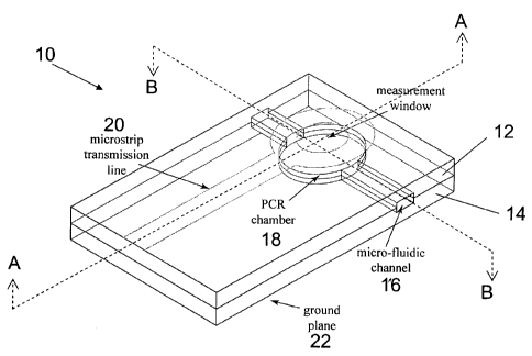
Figure 1 is a plan view of an embodiment of the present invention.
Figure 2 is a cross-sectional view along the A-A plane.
Figure 2 is a cross-sectional view along the B-B plane.
8
1 19620.00100/3 5 705 05 0 v.1
CA 02594277 2007-06-22
WO 2006/069305 PCT/US2005/046756
DETAILED DESCRIPTION OF THE PREFERRED EMBODIMENT
The present invention is generally directed to apparatuses and methods for
performing heating and/or thermocycling of small volume samples on a microchip
or
microfluidic apparatus using microwave radiation. The term "small volume" as
used
herein refers to volumes in the picoliters (pL) to microliters ( L) range,
preferably about
100 pL to about 100 L, most preferably about 1 nL to about 10 L. The term
"microfluidic" as used herein refers to an apparatus for analysis of small
volumes of
sample, and containing microscale components for fluid processing, such as
channels,
pumps, micro-reaction chambers, electrophoresis modules, microchannels, fluid
reservoirs, detectors, valves, or mixers. These microfluidic apparatuses are
also referred
to as micro-total analysis systems ( TAS). "Micro" as used herein refers to
small
components and is not restricted to micron or microliter scale, but also
include smaller
components in the nanometer or nanoliter range.
Applications of the microwave heating method of the present invention are
numerous and generally encompass any system in which the temperature of a
sample is
regulated and/or changed. The present invention is particularly applicable to
analytical
systems wherein fast or ultrafast transition from one temperature to the next
is needed,
and in which it is important that exact or nearly exact temperatures be
achieved.
For example, the present apparatus and methods are suitable for testing and
incubation and treatment of biological samples typically analyzed in a
molecular biology
laboratory or a clinical diagnostic setting. The accuracy of the heating
method of the
present invention makes it particularly suitable for use in nucleic acid
replication by the
polymerase chain reaction (PCR). Any reaction that benefits from precise
temperature
9
119620.00100/35 705050v.1
CA 02594277 2007-06-22
WO 2006/069305 PCT/US2005/046756
control, rapid heating and cooling, continuous thermal ramping or other
temperature
parameters or variations can be accomplished using this method discussed
herein. Other
applications include, but are not limited to, chemical reactions and
synthesis, the
activation and acceleration of enzymatic reactions, the deactivation of
enzymes, the
treatment/incubation of protein-protein complexes, nucleic acid-protein
complexes,
nucleic acid - nucleic acid complexes and complexes of any of these
biomolecules with
drugs and/or other organic or inorganic compounds to induce folding/unfolding
and the
association/dissociation of such complexes. The following applications
illustrate the
usefulness of the present thermocycling apparatus and methods, representing
only some
of the possible applications.
A common procedure in the protocols of molecular biology is the deactivation
of
proteins through heat. One of the most basic procedures in molecular biology
is the
cleavage of proteins and peptides into discrete fragments by
proteases/digestion enzymes,
such as trypsin. A thermocycling procedure is typically used to activate the
enzyme at an
elevated temperature followed by: the incubation of the enzyme during the
reaction to
sustain the enzymatic catalysis; the heat inactivation of the enzyme; and the
final
treatment/analysis at ambient temperature. Typically, the reaction components
are
incubated at 40 C for 60 minutes until the reaction is completed, after which
the enzyme
activity has to be stopped to avoid unspecific cleavage under uncontrolled
conditions.
Many enzymes, such as trypsin, can be irreversibly inactivated by incubation
for 10
minutes at higher temperature, such as 95 C. The sample is then cooled back to
ambient
temperature and ready for downstream analysis. Such deactivation of enzymes is
taught,
for example, in Sequencing of proteins and peptides: Laboratory Techniques in
119620.00100/3 5 705050v.1
CA 02594277 2007-06-22
WO 2006/069305 PCT/US2005/046756
Biochemistry and Molecular Biology, ed. G. Allen, pages 73-105.
The same principle of heat inactivation can be used to inactivate restriction
endonucleases that recognize short DNA sequences and cleave double stranded
DNA at
specific sites within or adjacent to the recognition sequence. Using the
appropriate assay
conditions (for example, 40 C for 60 min), the digestion reaction can be
completed in the
recommended time. The reaction is stopped by incubation of the sample at 65 C
for 10
minutes. Some enzymes may be partially or completely resistant to heat
inactivation at
65 C., but they may be inactivated by incubation for 15 minutes at 75 C. Such
methods
are taught, for example, by Ausubel et al. Short Protocols in Molecular
Biology, 3rd Ed.,
John Wiley & Sons, Inc. (1995) and Molecular Cloning: A Laboratory Manual, J.
Sambrook, Eds. E. F. Fritsch, T. Maniatis, 2nd Ed.
Similar to the heat inactivation of proteins for the control of enzymatic
activity,
the sample processing of proteins for electrophoretic analysis often requires
the
denaturation of the protein/peptide analyte before the separation by
electrophoretic means,
such as gel electrophoresis and capillary electrophoresis, takes place. For
example, a 5
minute heat denaturation (which provides for the destruction of the tertiary
and secondary
structure of the protein/peptide) at 95 C in an aqueous buffer in the presence
or absence
of denaturing reagents, such as SDS detergent, allows the size dependent
separation of
proteins and peptides by electrophoretic means. That is taught, for example,
in Gel
Electrophoresis of Proteins: A Practical Approach, Eds. B. D. Hames and D.
Rickwood,
page 47, Oxford University Press (1990).
Thermocycling of samples is also used in a number of nonenzymatic processes,
such as protein/peptide sequencing by hydrolysis in the presence of acids or
bases (for
11
119620.00100/35705050v.1
CA 02594277 2007-06-22
WO 2006/069305 PCT/US2005/046756
example, 6M HC1 at 110 C. for 24 hours) into amino acids. Studies involving
the
investigation of the interaction of biomolecules with drugs and/or drug
candidates are
frequently conducted under conditions requiring precise temperature control to
obtain
binding characteristics, such as kinetic association/dissociation constants.
Those applications for the heating and/or thermocycling taught by the present
invention will find use, for example, as a diagnostic tool in hospitals and
laboratories
such as for identifying specific genetic characteristics in a sample from a
patient, in
biotechnology research such as for the development of new drugs,
identification of
desirable genetic characteristics, etc., in biotechnology industry-wide
applications, in
chemical synthesis, or in medical research, e.g., investigating the effect of
microwave
frequencies on cells and biological molecules, and in other scientific
research and
development efforts.
The present invention provides a device and method for applying substantially
localized microwave radiation to samples in a microfluidic device. More
specifically, the
present invention provides microfluidic apparatuses or devices that have a
microwave
integrated circuit (MMIC) integrated into the device. The MMIC is used to
apply
microwave radiation to a micro-heating area or microwave radiation area
defined by the
device for enhancing or affecting a reaction or process taking place therein.
In addition,
as outlined herein, the devices of the invention can include, but is not
limited to, the
following components: one or more wells for sample manipulation, waste or
reagents;
microchannels to and between these wells, including microchannels containing
sampole
preparation or electrophoretic separation matrices; valves to control fluid
movement; and
12
119620.00100/35 705050v.1
CA 02594277 2007-06-22
WO 2006/069305 PCT/US2005/046756
on-chip pumps. The devices of the invention can be configured to manipulate
one or
multiple samples.
The MMIC designs of the present invention include, but are not limited to,
microstrip designs, slot designs, and coplanar designs. See, e.g., Gallium
Arsenide
Technology, Chs. 6-7 edited by David Kerry (Howard W. Sams & Co. 1985);
Microwave
Circuit Analysis and Amplifier Design, Liao S.(Prentice-Hall, 1987); Computer
Aided
Design of Microwave Circuits, Gupta et al. (Artech House 1981); all of which
are
incorporated herein by reference.
In a preferred embodiment, the MMIC designs of the present invention provide
high frequency absorption. By integration of an appropriate microwave circuit
into a
microfluidic device in accordance with the present invention, a precise,
reliable and
substantially localized application of microwave radiation to a sample in the
microfluidic
device is made possible. As the skilled artisan will appreciate, this enhances
or makes
possible many types of reactions and processes within a microfluidic device.
For
example, and without limitation, microwave irradiation has been shown to
improve
nucleic acid extraction from microorganisms, which is an essential step in
many
biochemical and biomedical.
Accordingly, the present invention provides MMIC devices. As used herein, the
term "monolithic microwave integrated circuit" or "MMIC" refers to a
combination of
interconnected microwave circuit elements integrated on a substrate.
The integrated circuits are on a substrate. The composition of the solid
substrate
will depend on a variety of factors, including the techniques used to create
the device, the
use of the device, the composition of the sample, the analyte to be detected,
the size of
13
119620.00100/3 5 705 05 0v.1
CA 02594277 2007-06-22
WO 2006/069305 PCT/US2005/046756
the wells and microchannels, the presence or absence of elecronic components,
etc.
Generally, the devices of the invention should be easily sterilizable as well.
The
integrated circuit and the fluidics maybe formed in the same substrate or in
different
substrates.
In a preferred embodiment, the solid substrate can be made from a wide variety
of
materials, including, but are not limited to, silicon such as silicon wafers,
silicon dioxide,
silicon nitride, ceramics, glass and fused silica, gallium arsenide, indium
phosphide,
aluminum, ceramics, polyimide, quartz, composite materials, fiberglass, FR-4,
plastics,
resins and polymers including polyimide, polymethylmethacrylate, acrylics,
polyethylene,
polyethylene terepthalate, polycarbonate, polystyrene and other styrene
copolymers,
polypropylene, polytetrafluoroethylene, superalloys, KOVAR, KEVLAR, KAPTON,
MYLAR, sapphire, etc. High quality glasses such as high melting borosilicate
or fused
silicas may be preferred for their UV transmission properties when any of the
sample
manipulation steps require light based technologies. In addition, as outlined
herein,
portions of the internal surfaces of the device may be coated with a variety
of coatings as
needed, to reduce non-specific binding, to allow the attachment of binding
ligands, for
biocompatibility, for flow resistance, etc. Most preferably, the substrates
are made from
glass or plastics.
There are many formats, materials, and size scales for constructing
microfluidic
devices. Common microfluidic devices are disclosed in U.S. Patent Nos.
6,692,700 to
Handique et al.; 6,919,046 to O'Connor et al.; 6,551,841 to Wilding et al.;
6,630,353 to
Parce et al.; 6,620,625 to Wolk et al.; and 6,517,234 to Kopf-Sill et al.; all
of which are
incorporated herein by reference. Typically, a microfludic device is made up
of two or
14
119620.00100/35 705050v.1
CA 02594277 2007-06-22
WO 2006/069305 PCT/US2005/046756
more substrates that are bonded together. Microscale components for processing
fluids
are disposed on a surface of one or more of the substrates. These microscale
components
include, but are not limited to, micro-reaction chambers, solid phase
extraction modules,
electrophoresis modules, microchannels, fluid reservoirs, detectors, valves,
or mixers.
When the substrates are bonded together, the microscale components are
enclosed and
sandwiched between the substrates. In many embodiments, at least inlet and
outlet ports
are engineered into the device for introduction and removal of fluid from the
system. The
microscale components can be linked together to form a fluid network for
chemical and
biological analysis. Those skilled in the art will recognize that substrates
composed of
silicon, glass, ceramics, plastics, polymers, metals and/or quartz are all
acceptable in the
context of the present invention. Further, the design and construction of the
microfluidic
network vary depending on the analysis being performed and are within the
ability of
those skilled in the art.
The devices may comprise conductors for the transmission of microwave
radiation. Suitable transmission lines include, but are not limited to,
microstrip line
conductors and slot line conductors, both of which are well known in the art.
The position, orientation and number of conductors can vary widely, as will be
appreciated by those in the art. In a preferred embodiment, the conductors are
placed
adjacent to the micro-area for which microwave radiation is desired. By
"adjacent"
herein is meant that the conductors are close enough to deliver microwave
radiation to the
sample within the desired micro-area.
In addition to the micro-heating or irradiation area, the devices of the
invention
can include other components, such as one or more wells for sample
manipulation, waste
119620.00100/35 705050v.1
CA 02594277 2007-06-22
WO 2006/069305 PCT/US2005/046756
or reagents; microchannels to and between these wells, including microchannels
containing sample preparation or electrophoretic separation matrices; valves
to control
fluid movement; on-chip pumps such as electroosmotic, electrohydrodynamic, or
electrokinetic pumps; and detection systems, such as optical or electrical
detection
systems. The devices of the invention can be configured to manipulate one or
multiple
samples or analytes. Any of these other microscale components can also be
heated as
well using a microwave circuit. A microfluidic chip may contain more than one
micro-
heating or irradiation areas.
In an embodiment, the solid substrate is configured for handling a single
sample
that may contain a plurality of target analytes. That is, a single sample is
added to the
device and the sample may either be aliquoted for parallel processing for
detection of the
analytes or the sample may be processed serially, with individual targets
being detected
in a serial fashion. In addition, samples may be removed periodically or from
different
locations for in line sampling.
In a preferred embodiment, the solid substrate is configured for handling
multiple
samples, each of which may contain one or more target analytes. In general, in
this
embodiment, each sample is handled individually; that is, the manipulations
and analyses
are done in parallel, with preferably no contact or contamination between
them.
Alternatively, there may be some steps in common; for example, it may be
desirable to
process different samples separately but detect all of the target analytes in
a single
detection region.
In addition, it should be understood that while most of the discussion herein
is
directed to the use of planar substrates with microchannels and wells, other
geometries
16
1196 20.00100/3 5 705 05 0v.1
CA 02594277 2007-06-22
WO 2006/069305 PCT/US2005/046756
can be used as well. For example, two or more planar substrates can be stacked
to
produce a three dimensional device, that can contain microchannels flowing
within one
plane or between planes; similarly, wells may span two or more substrates to
allow for
larger sample volumes. Thus for example, both sides of a substrate can be
etched to
contain microchannels; see for example U.S. Pat. Nos. 5,603,351 and 5,681,484,
both of
which are incorporated herein by reference.
Thus, the devices of the invention include at least one microchannel or flow
channel that allows the flow of sample from the sample inlet port to the other
components
or modules of the system. The collection of microchannels and wells is
sometimes
referred to in the art as either a "micro Total Analysis Systems" ( TAS) or
"mesoscale
flow system" when larger volumes are used. As will be appreciated by those in
the art,
the flow channels may be configured in a wide variety of ways, depending on
the use of
the channel. For example, a single flow channel starting at the sample inlet
port may be
separated into a variety of smaller channels, such that the original sample is
divided into
discrete sub-samples for parallel processing or analysis. Alternatively,
several flow
channels from different modules, for example the sample inlet port and a
reagent storage
module may feed together into a mixing chamber or a reaction chamber. As will
be
appreciated by those in the art, there are a large number of possible
configurations; what
is important is that the flow channels allow the movement of sample.and
reagents from
one part of the device to another. For example, the path lengths of the flow
channels may
be altered as needed; for example, when mixing and timed reactions are
required, longer
and sometimes tortuous flow channels can be used.
17
119620.00100/3 5705050v.1
CA 02594277 2007-06-22
WO 2006/069305 PCT/US2005/046756
In general, the microfluidic devices of the invention are generally referred
to as
microscale devices, but nanoscale or "mesoscale" devices could also be
employed. The
devices herein are typically designed on a scale suitable to analyze
microvolumes,
although in some embodiments large samples (e.g. cc's of sample) may be
reduced in the
device to a small volume for subsequent analysis. That is, "microscale" as
used herein
refers to chambers and microchannels that have cross-sectional areas on the
order of 0.1-
3000 m2. The microscale flow channels and wells have preferred depths on the
order of
0.1-500 .m. The channels have preferred widths on the order of 0.2-1000 m,
more
preferably 3-100 .m. For many applications, channels of 5-500 m are useful.
However,
for many applications, larger "mesoscale" dimensions on the scale of
millimeters may be
used. Similarly, chambers in the substrates often will have larger dimensions
than the
microchannels, on the scale of 1-3 mm (width and depth). When very small
sample
volumes may be used, nanoscale devices are useful.
In addition to the flow channel system, the devices of the invention are
configured
to include one or more of a variety of components that will be present on any
given
device depending on its use. These components include, but are not limited to,
sample
inlet ports; sample introduction or collection modules; cell handling modules
(for
example, for cell lysis (including the microwave lysis of cells as described
herein), cell
removal, cell concentration, cell separation or capture, cell growth, etc.);
separation
modules, for example, for electrophoresis, gel filtration, ion
exchange/affinity
chromatography (capture and release) etc.; reaction modules for chemical or
biological
reactions or alteration of the sample, including amplification of the target
analyte (for
example, when the target analyte is nucleic acid, amplification techniques are
useful,
18
11 9620.00100/35 705050v. I
CA 02594277 2007-06-22
WO 2006/069305 PCT/US2005/046756
including, but not limited to polymerase chain reaction (PCR), real-time PCR,
ligase
chain reaction (LCR), strand displacement amplification (SDA), whole genome
amphiplication (WGA), and nucleic acid sequence based amplification (NASBA)),
chemical, physical or enzymatic cleavage or alteration of the target analyte,
or chemical
modification of the target; fluid pumps; fluid valves; thermal modules for
heating and
cooling; storage modules for assay reagents; mixing chambers; and detection
modules.
The devices of the invention may include at least one sample inlet port for
the
introduction of the sample to the device. This may be part of or separate from
a sample
introduction or collection module; that is, the sample may be directly fed in
from the
sample inlet port to a separation chamber, or it may be pretreated in a sample
collection
well or chamber.
The devices of the invention may include a sample collection module, which can
be used to concentrate or enrich the sample if required; for example, see U.S.
Pat. No.
5,770,029, which is incorporated herein by reference.
The devices of the invention may include a cell handling module. This is
particularly useful when the sample comprises cells that either contain the
target analyte
or that must be removed in order to detect the target analyte. Thus, for
example, the
detection of particular antibodies in blood can require the removal of the
blood cells for
efficient analysis, or the cells (and/or nucleus) must be lysed prior to
detection. In this
context, "cells" include eukaryotic and prokaryotic cells as outlined herein,
and viral
particles that may require treatment prior to analysis, such as the release of
nucleic acid
from a viral particle prior to detection of target sequences. In addition,
cell handling
modules may also utilize a downstream means for determining the presence or
absence of
19
1 19620.00100/35705050v. 1
CA 02594277 2007-06-22
WO 2006/069305 PCT/US2005/046756
cells. Suitable cell handling modules include, but are not limited to, cell
lysis modules,
cell removal modules, cell concentration modules, and cell separation or
capture modules.
In addition, as for all the modules of the invention, the cell handling module
is in fluid
communication via a flow channel with at least one other module of the
invention.
In a preferred embodiment, the devices of the invention include a separation
module. This can comprise the separation or isolation of the target analyte,
or the
removal of contaminants that interfere with the analysis of the target
analyte, depending
on the assay. The separation module includes chromatographic-type separation
media
such as absorptive phase materials, including, but not limited to reverse
phase materials,
ion-exchange materials, affinity chromatography materials such as binding
ligands, etc.
See U.S. Pat. No. 5,770,029, which is incorporated herein by reference. The
separation
module can utilize binding ligands. In this embodiment, binding ligands are
preferably
immobilized (again, either by physical absorption or covalent attachment,
described
below) within the separation module (again, either on the internal surface of
the module,
on a particle such as a bead, filament or capillary trapped within the module,
for example
through the use of a frit). Suitable binding moieties will depend on the
sample
component to be isolated or removed. "Binding ligand" as used herein refers to
a
compound that is used to bind a component of the sample, either a contaminant
(for
removal) or the target analyte (for enrichment). The binding ligand can also
be used to
probe for the presence of the target analyte by binding to the analyte.
The devices of the invention may include a reaction chamber. This can include
either physical, chemical, or biological alteration of one or more sample
components.
Alternatively, it may include a reaction chamber wherein the target analyte
alters a
119620.00100/35705050v, I
CA 02594277 2007-06-22
WO 2006/069305 PCT/US2005/046756
second moiety that can then be detected; for example, if the target analyte is
an enzyme,
the reaction chamber may comprise an enzyme substrate that upon modification
by the
target analyte, can then be detected. In this embodiment, the reaction module
may
contain the necessary reagents, or they may be stored in a storage module and
pumped to
the reaction module as needed.
The devices of the invention may include a detection module used to detect
target
analytes in samples. By "target analyte" or "analyte" herein is meant to be
any molecule,
compound or particle to be detected. Target analytes preferably binds to
binding ligands,
as is more fully described above. The detection module can include detectors
that are
incorporated into the device or be aligned with a detector that is not
incorporated into the
device. In some instances, the detection section includes the flow channel in
which the
thermal cycling reaction takes place. In other designs, the detection section
is located at
another part of the device, typically downstream from an outlet connected to
the flow
channel in which thermal cycling occurs. Because the microfluidic devices
provided
herein can be made from optically transparent materials, the devices can be
used with
certain optical detection systems that cannot be utilized with conventional
devices
manufactured from silicon. A large number of analytes may be detected using
the
present methods; basically, any target analyte for which a binding ligand,
described
herein, may be made may be detected using the methods of the invention.
Detection
methods for PCR or other amplification-related reactions are disclosed in U.S.
Patent No.
6,960,437, which is incorporated herein by reference. As will be appreciated
by those in
the art, the particular detection method employed depends upon the nature of
the reactant
and/or product being detected.
21
1 19620.00100/35705050v. 1
CA 02594277 2007-06-22
WO 2006/069305 PCT/US2005/046756
The device of the present invention is preferably used in conjunction with an
apparatus for cooling, such as that disclosed by U.S. Patent No. 6,413,766 to
Landers et
al., which is incorporated herein by reference. Cooling to a desired
temperature can be
effected in one step, or in stepwise reductions with a suitable dwell time at
each
temperature step. Cooling can be accomplished by any methods available
including, but
are not limited to, forced air, contact cooling, Peltier cooling, passive
cooling, and
chemical cooling. Positive cooling is preferably effected by use of a non-
contact air
source that forces air at or across the vessel. Preferably, that air source is
a compressed
air source, although other sources could also be used. It will be understood
by those
skilled in the art that positive cooling results in a more rapid cooling than
simply
allowing the vessel to cool to the desired temperature by heat dissipation.
Cooling can be
accelerated by contacting the selected areas with a heat sink comprising a
larger surface
than the selected areas themselves; the heat sink is cooled through the non-
contact
cooling source. The cooling effect can also be more rapid if the air from the
non-contact
cooling source is at a lower temperature than ambient temperature.
Accordingly, the non-contact cooling source should also be positioned remotely
to the sample or reaction vessel, while being close enough to effect the
desired level of
heat dissipation. Both the heating and cooling sources should be positioned so
as to
cover the largest possible surface area on the sample vessel. The heating and
cooling
sources can be alternatively activated to control the temperature of the
sample. It will be
understood that more than one cooling source can be used.
Positive cooling of the reaction vessel dissipates heat more rapidly than the
use of
ambient air. The cooling means can be used alone or in conjunction with a heat
sink. A
22
119620.00100/35705050v.1
CA 02594277 2007-06-22
WO 2006/069305 PCT/US2005/046756
particularly preferred cooling source is a compressed air source. Compressed
air is
directed at the selected areas when cooling of the sample is desired through
use, for
example, of a solenoid valve which regulates the flow of compressed air at or
across the
selected areas. The pressure of the air leaving the compressed air source can
have a
pressure of anywhere between 10 and 60 PSI, for example. Higher or lower
pressures
could also be used. The temperature of the air can be adjusted to achieve the
optimum
performance in the thermocycling process. Although in most cases compressed
air at
ambient temperature can create enough of a cooling effect, the use of cooled,
compressed
air to more quickly cool the sample, or to cool the sample below ambient
temperature
might be desired in some applications.
A device for monitoring the temperature of the sample, and a device for
controlling the heating and cooling of the sample, may also be provided.
Generally, such
monitoring and controlling is accomplished by use of a microprocessor or
computer
programmed to monitor temperature and regulate or change temperature. An
example of
such a program is the Labview program (National Instruments, Austin, TX).
Feedback
from a temperature sensing device, such as a thermocouple or a remote
temperature
sensor, is sent to the computer. In one embodiment, the temperature sensing
device
provides an electrical input signal to the computer or other controller, which
signal
corresponds to the temperature of the sample. Preferably, the thermocouple,
which can
be coated or uncoated, is placed adjacent to the selected portions of the
microfluidic
device where rapid heating and/or cooling is desired. Alternatively, the
thermocouple
can be placed directly into the microscale component, provided that the
thermocouple
does not interfere with the particular reaction or affect the thermocycling,
and provided
23
1 19620.00100/35 705050v.1
CA 02594277 2007-06-22
WO 2006/069305 PCT/US2005/046756
that the thermocouple used does not act as a significant heat sink. A suitable
thermocouple for use with the present invention is constantan-copper
thermocouple.
In a preferred embodiment, temperature is monitored and controlled through a
remote temperature sensing means. For example, an optical sensing device can
be placed
above a reaction vessel containing the sample being thermocycled. Such a
device can
sense the temperature in a chamber or on the surface of the chamber, here the
sample
reaction chamber, when positioned remotely from the selected areas.
A microfluidic device of the present invention, in its simplest form is
illustrated in
Figures 1-3. The microfluidic device 10 includes top substrate 12, bottom
substrate 14,
and a microstrip MMIC, which is discussed in more detail below. The top and
bottom
substrates 12 and 14 defines a microchannel 16 and a chamber 18. The MMIC is
defined
by a microstrip transmission line 20 and ground plane conductor 22, together
with the
material between conductors 20 and 22. The microstrip transmission line 20 is
formed on
the top surface 26 of the microfluidic device 10; and the ground plane is
formed on the
bottom surface 28 of the microfluidic device 10.
As will be appreciated by the skilled artisan, the MMIC described herein have
a
microwave source connected thereto. Preferably, an amplifier and/or coupler is
connected between the microwave source and the MMIC in a manner known to the
skilled artisan. This source consists of a compact surface-mount microwave
oscillator
followed by a power amplifier chip capable of delivering on the order of 5 W.
The
source and power amplifier will operate within the frequency range of 500 MHz
to 10
GHz, preferably from about 800 MHz to 8 GHz, most preferably from about 1 GHz
to 5
GHz. This source preferably can be controlled rapidly through the use of high-
speed
24
1 19620.00100/35705050v.1
CA 02594277 2007-06-22
WO 2006/069305 PCT/US2005/046756
microwave switches capable of switching in the nanosecond time regime. The
microwave power will be delivered to the specific areas of the microdevice via
microstrip
transmission lines integrated onto or in close proximity to the chip. These
transmission
lines have very low loss and, with proper design, will allow efficient
delivery of the
microwave power directly into specific areas, such as an on-chip PCR chamber.
In
addition, microstrip transmission lines are very simple structures requiring a
solid metal
ground plane on one side of the chip and a metal strip on the other.
Therefore, the
addition of these transmission lines to a disposable chip will not add
significantly to the
overall chip cost. This miniature microwave power delivery can be applied to a
single
micro-area of the chip (e.g., a microchamber) but clearly can be extrapolated
to multiple
areas on the chip, with the only limitation being the density of micro-
structures.
For efficient delivery of microwave energy to the reaction chamber, it is
necessary to match the impedance of the filled reaction chamber to the
transmission line
impedance. As an example, we consider the case of a 1 L chamber filled with
pure
water.
At 25 C and 900 MHz, the complex permittivity of pure water is E=(78 -j3.4)
6 (where s is the permittivity of free space). It is the imaginary component
that
converts the microwave energy into heat. Using this value, an equivalent
resistance for
the microchamber, as seen by the transmission line, can be calculated as
follows:
a=(2n)(900 MHz)(3.4E o) = 0.168 S/m
R 1/(6 A)
For a 1 x 10"6 L cylindrical microchamber, the dimensions are
depth: l = 100 m
119620.00100/35705050v.1
CA 02594277 2007-06-22
WO 2006/069305 PCT/US2005/046756
radius: r = 1.9 mm (A =7irz = 11.3 x 10⁻⁶ m2)
This results in an equivalent resistance of:
R = 52.7 S2
This resistance is very close to the standard transmission line impedance used
for
microwave circuit design (50 SZ ). The significance of this is that it will be
possible to
deliver microwave power into the water within the microchamber very
efficiently.
In addition to this equivalent resistance there is also an equivalent
capacitance in
parallel due to the real component of the complex permittivity (78Eo). This
capacitance
can be tuned out, using an appropriate parallel inductance, in order to
maintain an
efficient match between the transmission line and the reaction chamber.
Additionally, a computer or on-chip CPU is preferably used to monitor the
parameters (such as temperature) in the chamber and control the microwave
source and
amplifier to achieve predetermined parameters for the chamber. This computer
can also
be used to control temperature and other parameters in operation of the
microfluidic
device.
The present invention also provides microfabrication processes for making
microfluidic devices that include MMICs. The devices of the invention can be
made in a
variety of ways, as will be appreciated by those skilled in the art. See for
example
W096/39260, directed to the formation of fluid-tight electrical conduits. U.S.
Pat. No.
5,747,169, directed to sealing; EP 0637996 B 1; EP 0637998 BI; W096/39260;
W097/16835; W098/13683; W097/16561; W097/43629; W096/39252; W096/15576;
W096/15450; W097/37755; and W097/27324; and U.S. Pat. Nos. 5,304,487;
5,071531;
5,061,336; 5,747,169; 5,296,375; 5,110,745; 5,587,128; 5,498,392; 5,643,738;
5,750,015;
26
119620.00100/35 705050v.1
CA 02594277 2007-06-22
WO 2006/069305 PCT/US2005/046756
5,726,026; 5,35,358; 5,126,022; 5,770,029; 5,631,337; 5,569,364; 5,135,627;
5,632,876;
5,593,838; 5,585,069; 5,637,469; 5,486,335; 5,755,942; 5,681,484; and
5,603,351, all of
which are incorporated herein by reference. Suitable fabrication techniques
again will
depend on the choice of substrate, but preferred methods include, but are not
limited to, a
variety of micromachining and microfabrication techniques, including film
deposition
processes such as spin coating, chemical vapor deposition, laser fabrication,
photolithographic and other etching techniques using either wet chemical
processes or
plasma processes, embossing, injection molding and bonding techniques (see
U.S. Pat.
No. 5,747,169, which is incorporated herein by reference). In addition, there
are printing
techniques for the creation of desired fluid guiding pathways; that is,
patterns of printed
material can permit directional fluid transport. See for example U.S. Pat. No.
5,795,453,
which is incorporated herein by reference.
Photolithographic methods of etching substrates are particularly well suited
for
the microfabrication of these substrates and are well known in the art. For
example, the
first sheet of a substrate may be overlaid with a photoresist. Radiation may
be applied
through a photolithographic mask to expose the photoresist in a pattern which
reflects the
pattern of chambers and/or channels on the surface of the sheet. After
removing the
exposed photoresist, the exposed substrate may be etched to produce the
desired wells
and channels. Generally preferred photoresists include those used extensively
in the
semi-conductor industry. Such materials include polymethyl methacrylate (PMMA)
and
its derivatives, and electron beam resists, such as polyolefin sulfones and
the like (more
fully discussed in, e.g., Ghandi, "VLSI Fabrication Principles," Wiley (1983)
Chapter 10,
which is incorporated herein by reference).
27
119620.00100/3 5 70505 0v.1
CA 02594277 2007-06-22
WO 2006/069305 PCT/US2005/046756
Although certain presently preferred embodiments of the invention have been
specifically described herein, it will be apparent to those skilled in the art
to which the
invention pertains that variations and modifications of the various
embodiments shown
and described herein may be made without departing from the spirit and scope
of the
invention. Accordingly, it is intended that the invention be limited only to
the extent
required by the appended claims and the applicable rules of law.
28
119620.00100/35 705050v.1